


CD74HCT640M
Texas Instruments CD74HCT640M, CD74HCT640E, CD74HC640M, CD74HC640E, CD54HCT640F3A Datasheet
...
1
Data sheet acquired from Harris Semiconductor
SCHS192
Features
• Buffered Inputs
• Three-State Outputs
• Applications in Multiple-Data-Bus Architecture
• Fanout (Over Temperature Range)
- Standard Outputs. . . . . . . . . . . . . . . 10 LSTTL Loads
- Bus Driver Outputs . . . . . . . . . . . . . 15 LSTTL Loads
• Wide Operating Temperature Range . . . -55
o
C to 125
o
C
• Balanced Propagation Delay and Transition Times
• Significant Power Reduction Compared to LSTTL
Logic ICs
• HC Types
- 2V to 6V Operation
- High Noise Immunity: N
IL
= 30%, N
IH
= 30% of V
CC
at V
CC
= 5V
• HCT Types
- 4.5V to 5.5V Operation
- Direct LSTTL Input Logic Compatibility,
V
IL
= 0.8V (Max), V
IH
= 2V (Min)
- CMOS Input Compatibility, I
l
≤ 1µA at V
OL
, V
OH
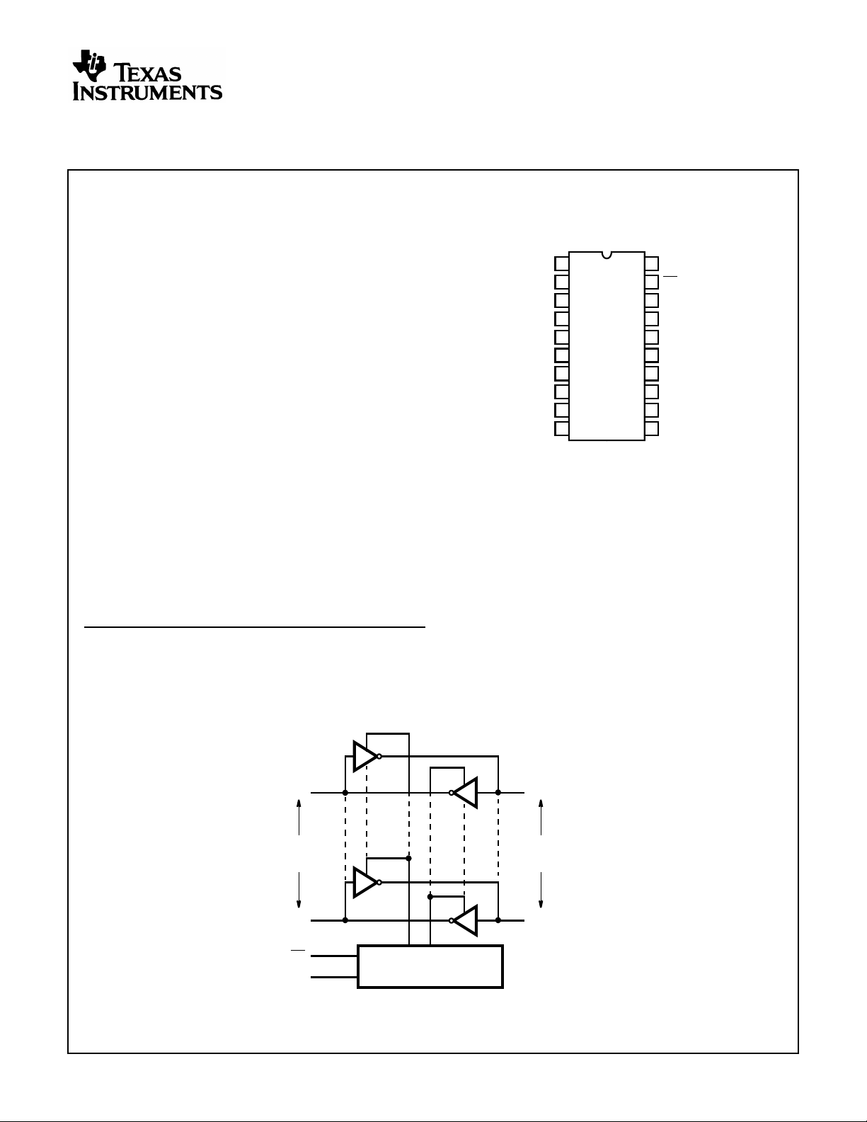
Pinout
CD74HC640, CD74HCT640
(PDIP, SOIC)
TOP VIEW
Description
The Harris CD74HC640 and CD74HCT640 silicon-gate
CMOS three-state bidirectional inverting and non-inverting
buffers are intended for two-way asynchronous
communication between data buses. They have high drive
current outputs which enable high-speed operation when
driving large bus capacitances. These circuits possess the
low power dissipation of CMOS circuits, and have speeds
comparable to low power Sckottky TTL circuits. They can
drive 15 LSTTL loads. The CD74HC640 and CD74HCT640
are inverting buffers.
Functional Diagram
11
12
13
14
15
16
17
18
20
19
10
9
8
7
6
5
4
3
2
1
DIR
A0
A1
A2
A3
A4
A6
A5
A7
GND
V
CC
B0
B1
B2
OE
B3
B4
B5
B6
B7
OUTPUT ENABLE AND
DIRECTION-SELECT LOGIC
A0
A7
OE
DIR
B0
B7
A1
THRU
A6
B1
THRU
B6
V
CC
= 20
GND = 10
January 1998
CAUTION: These devices are sensitive to electrostatic discharge. Users should follow proper IC Handling Procedures.
Copyright
© Harris Corporation 1998
File Number 1677.1
CD74HC640,
CD74HCT640
High Speed CMOS Logic
Octal Three-State Bus Transceiver, Inverting
[ /Title
(CD74
HC640
,
CD74
HCT64
0)
/
Sub-
j
ect
(High
Speed
CMOS
2
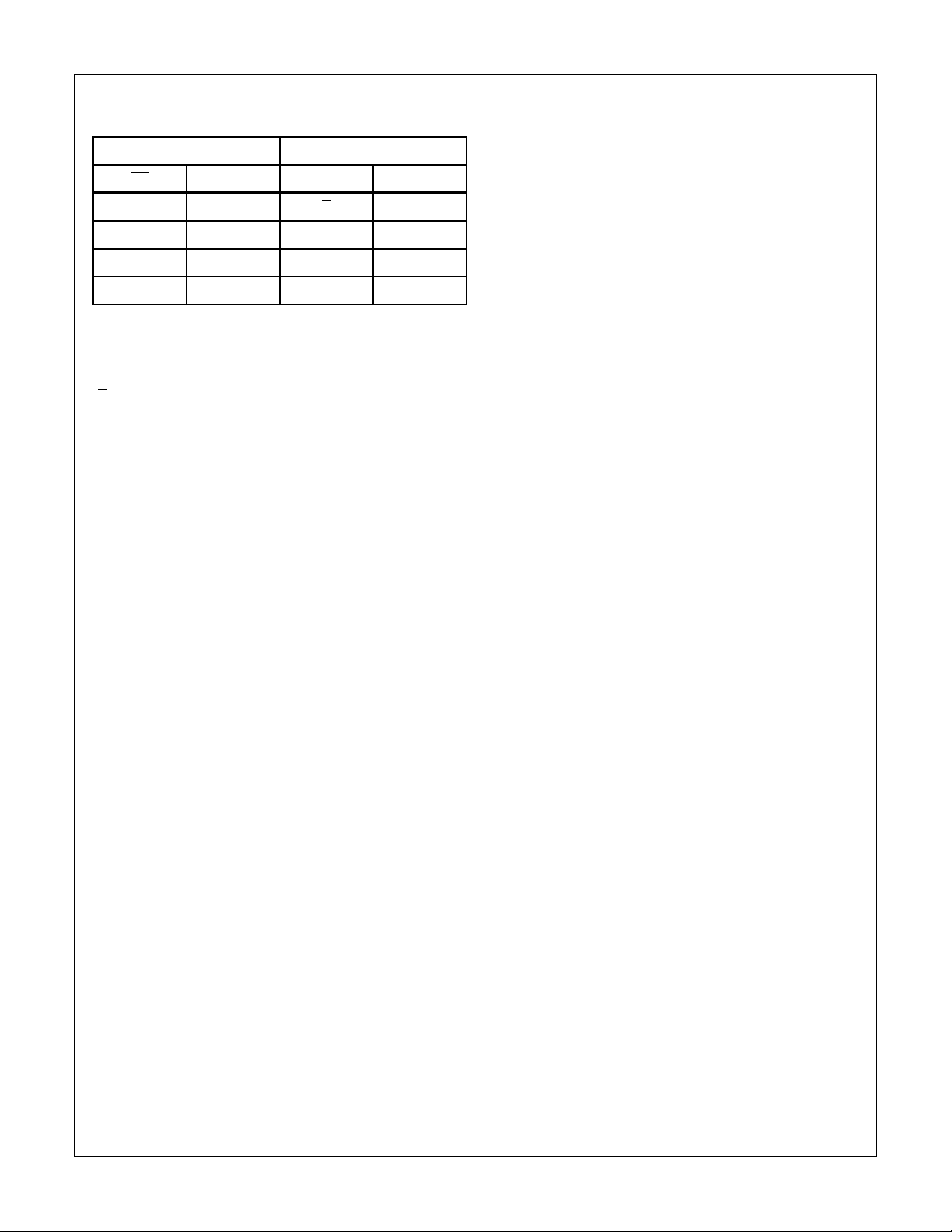
TRUTH TABLE
CONTROL INPUTS DATA PORT STATUS
OE DIR A
n
B
n
LLOI
HHZZ
HLZZ
LHIO
To prevent excess currents in the High-Z modes all I/O terminals
should be terminated with 1kΩ to 1MΩ resistors.
H = High Level
L = Low Level
I = Input
O = Output (Inversion of Input Level)
Z = High Impedance
CD74HC640, CD74HCT640CD74HC640, CD74HCT640
3
Absolute Maximum Ratings Thermal Information
DC Supply Voltage, V
CC
. . . . . . . . . . . . . . . . . . . . . . . . -0.5V to 7V
DC Input Diode Current, I
IK
For V
I
< -0.5V or V
I
> V
CC
+ 0.5V. . . . . . . . . . . . . . . . . . . . . .±20mA
DC Output Diode Current, I
OK
For V
O
< -0.5V or V
O
> V
CC
+ 0.5V . . . . . . . . . . . . . . . . . . . .±20mA
DC Drain Current, per Output, I
O
For -0.5V < V
O
< V
CC
+ 0.5V. . . . . . . . . . . . . . . . . . . . . . . . . .±35mA
DC Output Source or Sink Current per Output Pin, I
O
For V
O
> -0.5V or V
O
< V
CC
+ 0.5V . . . . . . . . . . . . . . . . . . . .±25mA
DC V
CC
or Ground Current, I
CC
. . . . . . . . . . . . . . . . . . . . . . . . .±50mA
Operating Conditions
Temperature Range, T
A
. . . . . . . . . . . . . . . . . . . . . . -55
o
C to 125
o
C
Supply Voltage Range, V
CC
HC Types . . . . . . . . . . . . . . . . . . . . . . . . . . . . . . . . . . . . .2V to 6V
HCT Types . . . . . . . . . . . . . . . . . . . . . . . . . . . . . . . . .4.5V to 5.5V
DC Input or Output Voltage, V
I
, V
O
. . . . . . . . . . . . . . . . . 0V to V
CC
Input Rise and Fall Time
2V . . . . . . . . . . . . . . . . . . . . . . . . . . . . . . . . . . . . . . 1000ns (Max)
4.5V. . . . . . . . . . . . . . . . . . . . . . . . . . . . . . . . . . . . . . 500ns (Max)
6V . . . . . . . . . . . . . . . . . . . . . . . . . . . . . . . . . . . . . . . 400ns (Max)
Thermal Resistance (Typical, Note 2) θ
JA
(
o
C/W)
PDIP Package. . . . . . . . . . . . . . . . . . . . . . . . . . . . . 125
SOIC Package. . . . . . . . . . . . . . . . . . . . . . . . . . . . . 120
Maximum Junction Temperature. . . . . . . . . . . . . . . . . . . . . . .150
o
C
Maximum Storage Temperature Range . . . . . . . . . .-65
o
C to 150
o
C
Maximum Lead Temperature (Soldering 10s). . . . . . . . . . . . .300
o
C
(SOIC - Lead Tips Only)
CAUTION: Stresses above those listed in “Absolute Maximum Ratings” may cause permanent damage to the device. This is a stress only rating and operation
of the device at these or any other conditions above those indicated in the operational sections of this specification is not implied.
NOTE:
7. θ
JA
is measured with the component mounted on an evaluation PC board in free air.
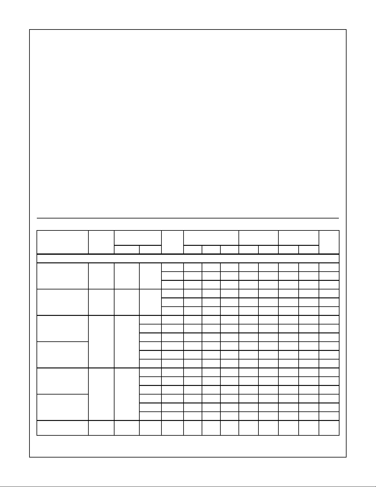
DC Electrical Specifications
PARAMETER SYMBOL
TEST
CONDITIONS
V
CC
(V)
25
o
C -40
o
C TO 85
o
C -55
o
CTO125
o
C
UNITSV
I
(V) I
O
(mA) MIN TYP MAX MIN MAX MIN MAX
HC TYPES
High Level Input
Voltage
V
IH
- - 2 1.5 - - 1.5 - 1.5 - V
4.5 3.15 - - 3.15 - 3.15 - V
6 4.2 - - 4.2 - 4.2 - V
Low Level Input
Voltage
V
IL
- - 2 - - 0.5 - 0.5 - 0.5 V
4.5 - - 1.35 - 1.35 - 1.35 V
6 - - 1.8 - 1.8 - 1.8 V
High Level Output
Voltage
CMOS Loads
V
OH
V
IH
or V
IL
-0.02 2 1.9 - - 1.9 - 1.9 - V
-0.02 4.5 4.4 - - 4.4 - 4.4 - V
-0.02 6 5.9 - - 5.9 - 5.9 - V
High Level Output
Voltage
TTL Loads
- - ---- - - - V
-6 4.5 3.98 - - 3.84 - 3.7 - V
-7.8 6 5.48 - - 5.34 - 5.2 - V
Low Level Output
Voltage
CMOS Loads
V
OL
V
IH
or V
IL
0.02 2 - - 0.1 - 0.1 - 0.1 V
0.02 4.5 - - 0.1 - 0.1 - 0.1 V
0.02 6 - - 0.1 - 0.1 - 0.1 V
Low Level Output
Voltage
TTL Loads
- - ---- - - - V
6 4.5 - - 0.26 - 0.33 - 0.4 V
7.8 6 - - 0.26 - 0.33 - 0.4 V
Input Leakage
Current
I
I
V
CC
or
GND
-6--±0.1 - ±1-±1µA
CD74HC640, CD74HCT640CD74HC640, CD74HCT640
 Loading...