


CD74HCT21M96
Texas Instruments CD74HCT21M96, CD74HCT21M, CD74HCT21E, CD74HC21M96, CD74HC21M Datasheet
...
CD74HC21,
/
[ /Title
(CD74H
C21,
CD74H
CT21)
Subject
(High
Speed
CMOS
Logic
Dual 4Input
Data sheet acquired from Harris Semiconductor
SCHS131
August 1997
Features
• Buffered Inputs
• Typical Propagation Delay: 9ns at V
C
= 15pF, TA = 25oC
L
• Fanout (Over Temperature Range)
- Standard Outputs. . . . . . . . . . . . . . . 10 LSTTL Loads
- Bus Driver Outputs . . . . . . . . . . . . . 15 LSTTL Loads
• Wide Operating Temperature Range . . . -55
• Balanced Propagation Delay and Transition Times
• Significant Power Reduction Compared to LSTTL
Logic ICs
• HC Types
- 2V to 6V Operation
- High Noise Immunity: N
at VCC = 5V
• HCT Types
- 4.5V to 5.5V Operation
- Direct LSTTL Input Logic Compatibility,
V
= 0.8V (Max), VIH = 2V (Min)
IL
- CMOS Input Compatibility, I
= 30%, NIH = 30% of V
IL
≤ 1µA at VOL, V
l
CC
= 5V,
o
C to 125oC
CC
OH
CD74HCT21
High Speed CMOS Logic
Dual 4-Input AND Gate
Description
The Harris CD74HC21, CD74HCT21, logic gates utilize
silicon gate CMOS technology to achieve operating speeds
similar to LSTTL gates with the low power consumption of
standard CMOS integrated circuits. All devices have the
ability to drive 10 LSTTL loads. The 74HCT logic family is
functionally pin compatible with the standard 74LS logic
family.
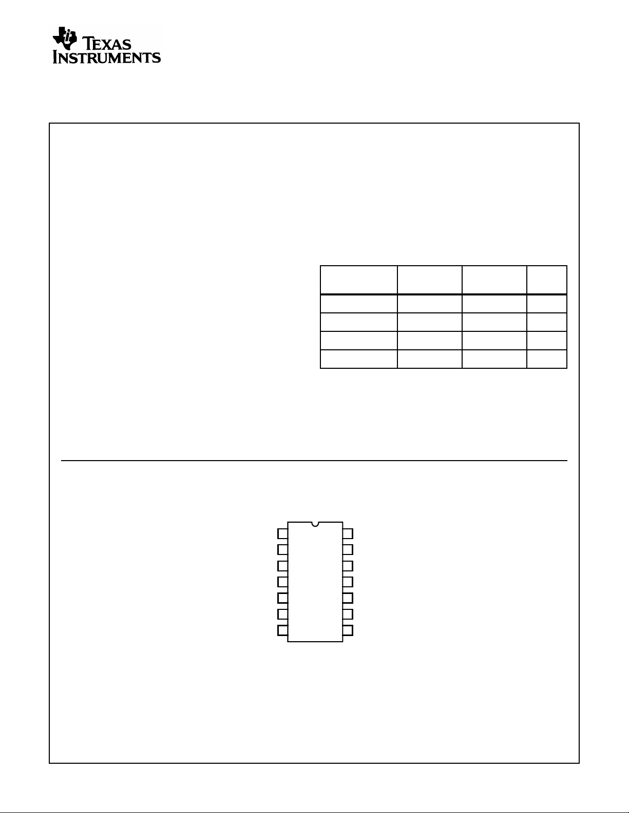
Ordering Information
TEMP.RANGE
PART NUMBER
CD74HC21E -55 to 125 14 Ld PDIP E14.3
CD74HCT21E -55 to 125 14 Ld PDIP E14.3
CD74HC21M -55 to 125 14 Ld SOIC M14.15
CD74HCT21M -55 to 125 14 Ld SOIC M14.15
NOTES:
1. When ordering, use the entire part number.Add the suffix 96 to
obtain the variant in the tape and reel.
2. Die for this part number is available which meets all electrical
specifications. Please contact your local sales office or Harris
customer service for ordering information.
(oC) PACKAGE
PKG.
NO.
Pinout
CD74HC21, CD74HCT21
(PDIP, SOIC)
TOP VIEW
1A
1
2
1B
3
NC
4
1C
5
1D
6
1Y
7
GND
14
V
CC
2D
13
12
2C
NC
11
2B
10
2A
9
2Y
8
CAUTION: These devices are sensitive to electrostatic discharge. Users should follow proper IC Handling Procedures.
Copyright
© Harris Corporation 1997
1
File Number 1782.1
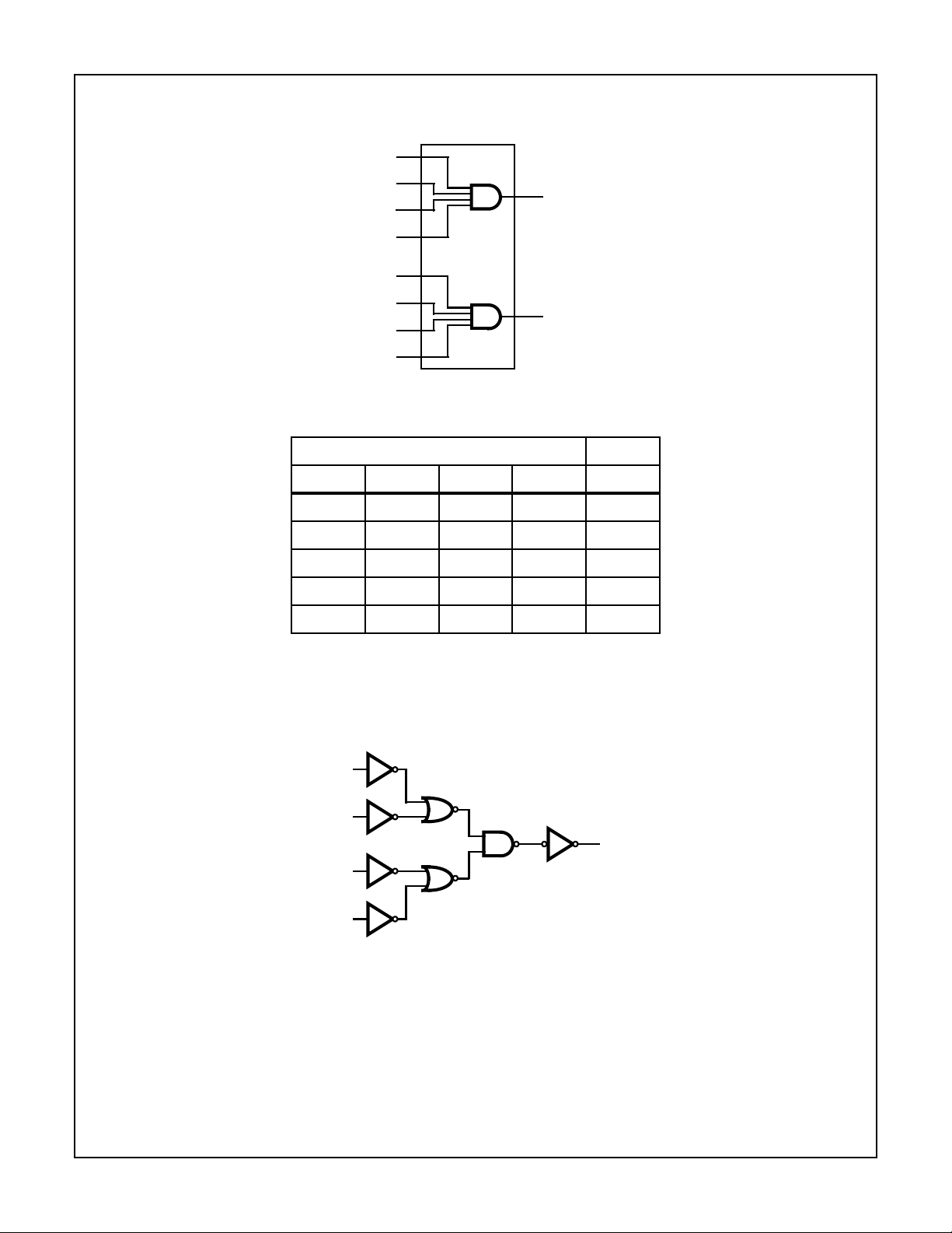
Functional Diagram
CD74HC21, CD74HCT21
1
1A
2
1B
4
1C
5
1D
9
2A
10
2B
12
2C
13
2D
TRUTH TABLE
INPUTS OUTPUT
nA nB nC nD nY
LXXXL
6
1Y
8
2Y
GND = 7
= 14
V
CC
NC = 3, 11
Logic Symbol
XLXXL
XXLXL
XXXLL
HHHHH
NOTE: H = High Voltage Level, L = Low Voltage Level,
X = Irrelevant
nA
nB
nY
nC
nD
2
 Loading...