


CD74HCT541M96
Texas Instruments CD74HCT541M96, CD74HCT541M, CD74HCT541E, CD74HCT540M96, CD74HCT540M Datasheet
...
1
Data sheet acquired from Harris Semiconductor
SCHS189
Features
• CD74HC540, CD74HCT540 . . . . . . . . . . . . . . . Inverting
• CD74HC541, CD74HCT541 . . . . . . . . . . . . . .Non-Inverting
• Buffered Inputs
• Three-State Outputs
• Bus Line Driving Capability
• Typical Propagation Delay = 9ns at V
CC
= 5V,
C
L
= 15pF, T
A
= 25
o
C
• Fanout (Over Temperature Range)
- Standard Outputs. . . . . . . . . . . . . . . 10 LSTTL Loads
- Bus Driver Outputs . . . . . . . . . . . . . 15 LSTTL Loads
• Wide Operating Temperature Range . . . -55
o
C to 125
o
C
• Balanced Propagation Delay and Transition Times
• Significant Power Reduction Compared to LSTTL
Logic ICs
• HC Types
- 2V to 6V Operation
- High Noise Immunity: N
IL
= 30%, N
IH
= 30% of V
CC
at V
CC
= 5V
• HCT Types
- 4.5V to 5.5V Operation
- Direct LSTTL Input Logic Compatibility,
V
IL
= 0.8V (Max), V
IH
= 2V (Min)
- CMOS Input Compatibility, I
l
≤ 1µA at V
OL
, V
OH
Description
The Harris CD74HC540 and CD74HCT540 are Inverting
Octal Buffers and Line Drivers with Three-State Outputs and
the capability to drive 15 LSTTL loads. The Harris
CD74HC541 and CD74HCT541 are Non-Inverting Octal Buff-
ers and Line Drivers with Three-State Outputs that can drive
15 LSTTL loads. The Output Enables (
OE1) and (OE2) con-
trol the Three-State Outputs. If either
OE1 or OE2 is HIGH the
outputs will be in the high impedance state. For data output
OE1 and OE2 both must be LOW.
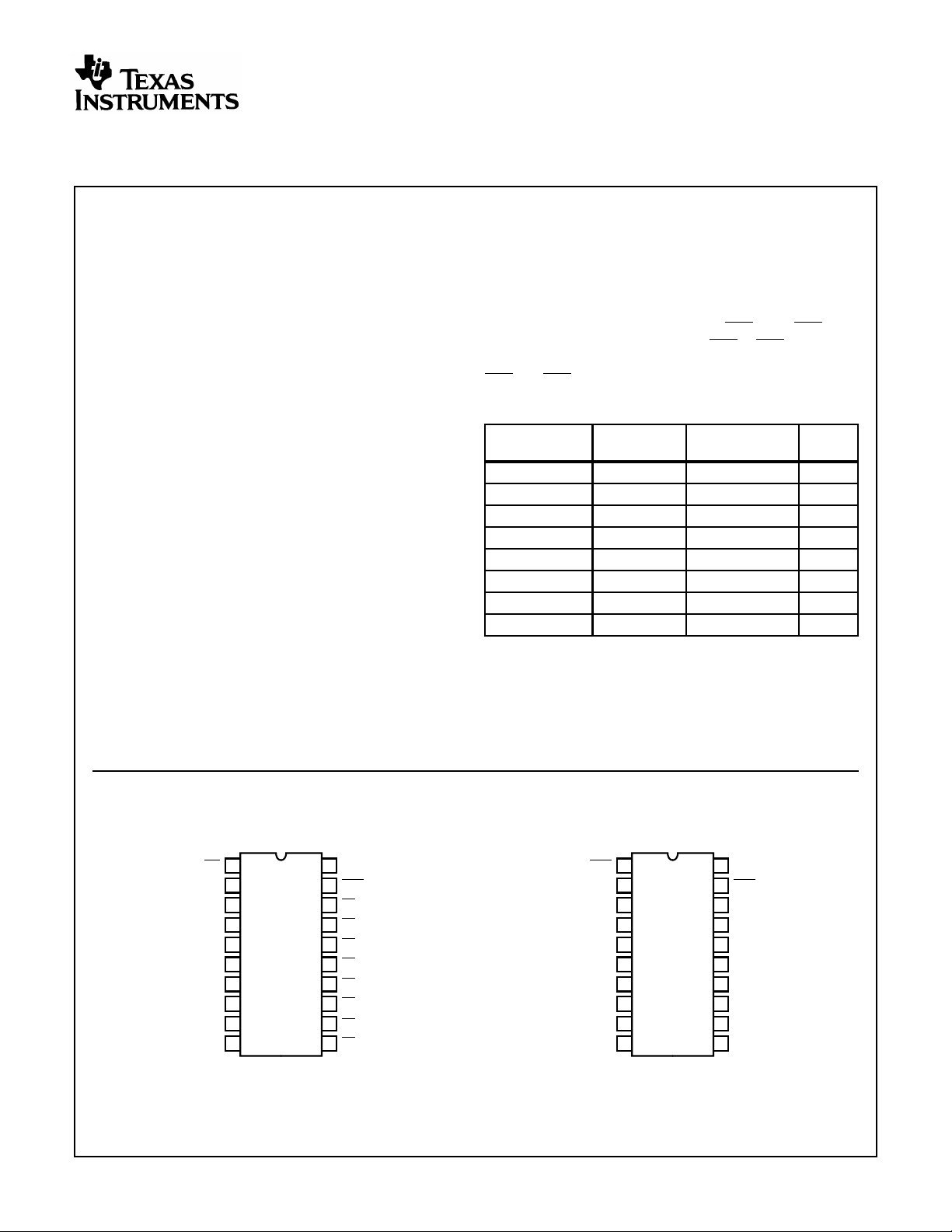
Ordering Information
PART NUMBER
TEMP.
RANGE (
o
C) PACKAGE
PKG.
NO.
CD74HC540E -55 to 125 20 Ld PDIP E20.3
CD74HCT540E -55 to 125 20 Ld PDIP E20.3
CD74HC541E -55 to 125 20 Ld PDIP E20.3
CD74HCT541E -55 to 125 20 Ld PDIP E20.3
CD74HC540M -55 to 125 20 Ld SOIC M20.3
CD74HCT540M -55 to 125 20 Ld SOIC M20.3
CD74HC541M -55 to 125 20 Ld SOIC M20.3
CD74HCT541M -55 to 125 20 Ld SOIC M20.3
NOTES:
1. When ordering, use the entire partnumber. Add thesuffix 96 to
obtain the variant in the tape and reel.
2. Wafer and die forthis part number is availablewhich meets all
electrical specifications.Please contact yourlocal sales office or
Harris customer service for ordering information.
Pinouts
CD74HC540, CD74HCT540
(PDIP, SOIC)
TOP VIEW
CD74HC541, CD74HCT541
(PDIP, SOIC)
TOP VIEW
11
12
13
14
15
16
17
18
20
19
10
9
8
7
6
5
4
3
2
1
OE
A0
A1
A2
A3
A4
A6
A5
A7
GND
V
CC
Y0
Y1
Y2
OE2
Y3
Y4
Y5
Y6
Y7 11
12
13
14
15
16
17
18
20
19
10
9
8
7
6
5
4
3
2
1
OE1
A0
A1
A2
A3
A4
A6
A5
A7
GND
V
CC
Y0
Y1
Y2
OE2
Y3
Y4
Y5
Y6
Y7
January 1998
CAUTION: These devices are sensitive to electrostatic discharge. Users should follow proper IC Handling Procedures.
Copyright
© Harris Corporation 1998
File Number 1659.2
CD74HC540, CD74HCT540,
CD74HC541, CD74HCT541
High Speed CMOS Logic
Octal Buffer and Line Drivers, Three-State
[ /Title
(CD74
HC540
,
CD74
HCT54
0,
CD74
HC541
,
CD74
HCT54
2
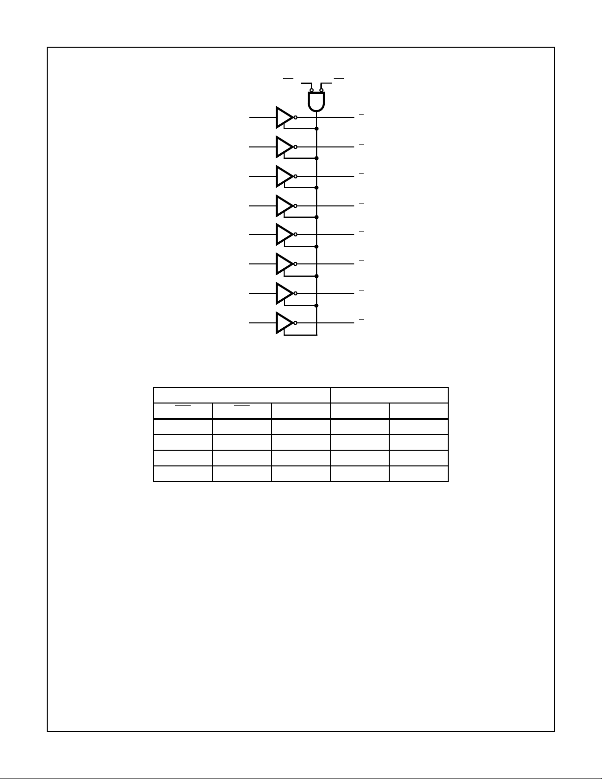
Functional Diagram
TRUTH TABLE
INPUTS OUTPUTS
OE1 OE2 An 540 541
LLHLH
HXXZZ
XHXZZ
LLLHL
NOTE:
H = HIGH Voltage Level
L = LOW Voltage Level
X = Don’t Care
Z = High Impedance
D
0
Y
0
D
2
D
4
D
6
Y
2
Y
4
Y
6
D
1
D
3
D
5
D
7
Y
1
Y
3
Y
5
Y
7
OE
A
OE
B
540 541
Y
0
Y
2
Y
4
Y
6
Y
1
Y
3
Y
5
Y
7
CD74HC540, CD74HCT540, CD74HC541, CD74HCT541CD74HC540, CD74HCT540, CD74HC541, CD74HCT541
3
Absolute Maximum Ratings Thermal Information
DC Supply Voltage, V
CC
. . . . . . . . . . . . . . . . . . . . . . . . -0.5V to 7V
DC Input Diode Current, I
IK
For V
I
< -0.5V or V
I
> V
CC
+ 0.5V. . . . . . . . . . . . . . . . . . . . . .±20mA
DC Output Diode Current, I
OK
For V
O
< -0.5V or V
O
> V
CC
+ 0.5V . . . . . . . . . . . . . . . . . . . .±20mA
DC Drain Current, per Output, I
O
For -0.5V < V
O
< V
CC
+ 0.5V. . . . . . . . . . . . . . . . . . . . . . . . . .±35mA
DC Output Source or Sink Current per Output Pin, I
O
For V
O
> -0.5V or V
O
< V
CC
+ 0.5V . . . . . . . . . . . . . . . . . . . .±25mA
DC V
CC
or Ground Current, I
CC
. . . . . . . . . . . . . . . . . . . . . . . . .±50mA
Operating Conditions
Temperature Range, T
A
. . . . . . . . . . . . . . . . . . . . . . -55
o
C to 125
o
C
Supply Voltage Range, V
CC
HC Types . . . . . . . . . . . . . . . . . . . . . . . . . . . . . . . . . . . . .2V to 6V
HCT Types . . . . . . . . . . . . . . . . . . . . . . . . . . . . . . . . .4.5V to 5.5V
DC Input or Output Voltage, V
I
, V
O
. . . . . . . . . . . . . . . . . 0V to V
CC
Input Rise and Fall Time
2V . . . . . . . . . . . . . . . . . . . . . . . . . . . . . . . . . . . . . . 1000ns (Max)
4.5V. . . . . . . . . . . . . . . . . . . . . . . . . . . . . . . . . . . . . . 500ns (Max)
6V . . . . . . . . . . . . . . . . . . . . . . . . . . . . . . . . . . . . . . . 400ns (Max)
Thermal Resistance (Typical, Note 3) θ
JA
(
o
C/W)
PDIP Package. . . . . . . . . . . . . . . . . . . . . . . . . . . . . 125
SOIC Package. . . . . . . . . . . . . . . . . . . . . . . . . . . . . 120
Maximum Junction Temperature. . . . . . . . . . . . . . . . . . . . . . . 150
o
C
Maximum Storage Temperature Range . . . . . . . . . .-65
o
C to 150
o
C
Maximum Lead Temperature (Soldering 10s). . . . . . . . . . . . . 300
o
C
(SOIC - Lead Tips Only)
CAUTION: Stresses above those listed in “Absolute Maximum Ratings” may cause permanent damage to the device. This is a stress only rating and operation
of the device at these or any other conditions above those indicated in the operational sections of this specification is not implied.
NOTE:
3. θ
JA
is measured with the component mounted on an evaluation PC board in free air.
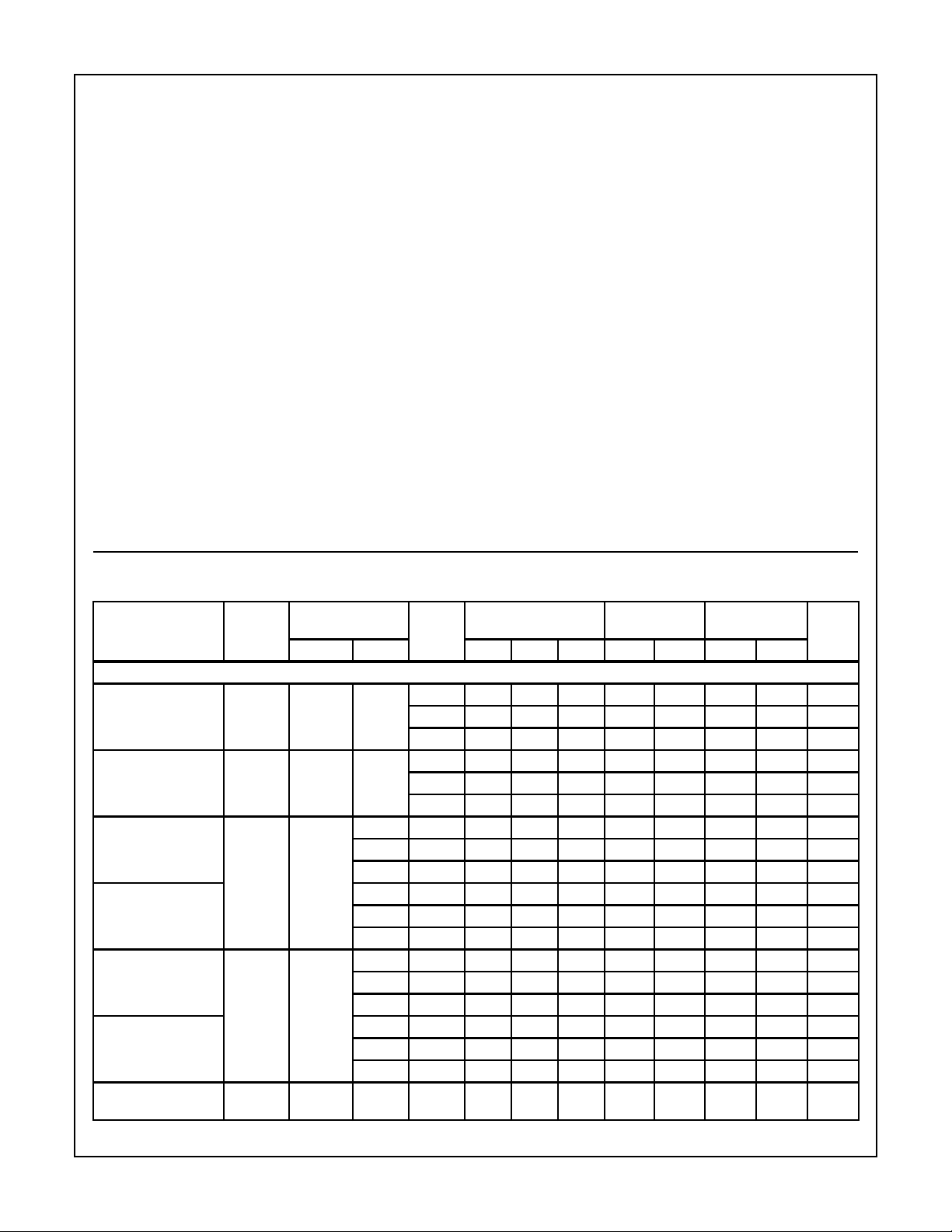
DC Electrical Specifications
PARAMETER SYMBOL
TEST
CONDITIONS
V
CC
(V)
25
o
C -40
o
C TO 85
o
C -55
o
CTO125
o
C
UNITSV
I
(V) I
O
(mA) MIN TYP MAX MIN MAX MIN MAX
HC TYPES
High Level Input
Voltage
V
IH
- - 2 1.5 - - 1.5 - 1.5 - V
4.5 3.15 - - 3.15 - 3.15 - V
6 4.2 - - 4.2 - 4.2 - V
Low Level Input
Voltage
V
IL
- - 2 - - 0.5 - 0.5 - 0.5 V
4.5 - - 1.35 - 1.35 - 1.35 V
6 - - 1.8 - 1.8 - 1.8 V
High Level Output
Voltage
CMOS Loads
V
OH
V
IH
or V
IL
-0.02 2 1.9 - - 1.9 - 1.9 - V
-0.02 4.5 4.4 - - 4.4 - 4.4 - V
-0.02 6 5.9 - - 5.9 - 5.9 - V
High Level Output
Voltage
TTL Loads
- - ---- - - - V
-6 4.5 3.98 - - 3.84 - 3.7 - V
-7.8 6 5.48 - - 5.34 - 5.2 - V
Low Level Output
Voltage
CMOS Loads
V
OL
V
IH
or V
IL
0.02 2 - - 0.1 - 0.1 - 0.1 V
0.02 4.5 - - 0.1 - 0.1 - 0.1 V
0.02 6 - - 0.1 - 0.1 - 0.1 V
Low Level Output
Voltage
TTL Loads
- - ---- - - - V
6 4.5 - - 0.26 - 0.33 - 0.4 V
7.8 6 - - 0.26 - 0.33 - 0.4 V
Input Leakage
Current
I
I
V
CC
or
GND
-6--±0.1 - ±1-±1µA
CD74HC540, CD74HCT540, CD74HC541, CD74HCT541CD74HC540, CD74HCT540, CD74HC541, CD74HCT541
 Loading...