


CY74FCT163543CPVCT
Texas Instruments CY74FCT163543CPVCT, CY74FCT163543CPVC, CY74FCT163543CPAC, CY74FCT163543APVCT, CY74FCT163543APVC Datasheet
16-Bit Latched Transceiver
CY74FCT163543
SCCS063A - June 1997 - Revised April 2000
Data sheet acquired from Cypress Semiconductor Corporation.
Data sheet modified to remove devices not offered.
Copyright © 2000, Texas Instruments Incorporated
1CY74FCT163543
Features
• Low power, pin-compatible replacement for LCX and
LPT families
• 5V tolerant inputs and outputs
• 24 mA balanced drive outputs
• Power-off disable outputs permits live insertion
• Edge-rate control circuitry for reduced noise
• FCT-C speed at 5.1 ns
• Latch-up performance exceedsJEDEC standard no. 17
• ESD > 2000V per MIL-STD-883D, Method 3015
• Typical output skew < 250 ps
• Industrial temperature range of –40˚C to +85˚C
• TSSOP (19.6-mil pitch) or SSOP (25-mil pitch)
• TypicalV
olp
(groundbounce)performanceexceedsMil
Std 883D
•V
CC
= 2.7V to 3.6V
Functional Description
The CY74FCT163543 is a 16-bit, high-speed, low power latched
transceiverthatisorganizedastwoindependent 8-bitD-type latched
transceivers,containingtwosetsof eightD-typelatches withseparate
LatchEnable(
LEAB,LEAB)and OutputEnable (OEAB,OEAB) con-
trols for each set to permit independent control of inputting and out-
putting in either direction of data flow . For data flow from A to B, for
example, the A-to-B input Enable (
CEAB) must be LOW in order to
enterdata fromA orto takedata fromB, asindicated inthe truth table.
With
CAEB LOW ,a LOWsignal on the A-to-BLatch Enable(LEAB)
makes the A-to-B latches transparent; a subsequent LOW-to-HIGH
transition of the
LEAB signal putsthe A latches in the storage mode
andtheiroutputs nolonger followtheA inputs.With
CEABandOEAB
both LOW,the three-state B output buffersare activeand reflect the
data present at the output of the A latches. Control of data from B to
A is similar, but uses
CEAB, LEAB, and OEAB inputs.
The CY74FCT163543 has 24-mA balanced output drivers
with current limiting resistors in the outputs. This reduces the
need for external terminating resistors and provides for
minimal undershoot and reduced ground bounce. The inputs
and outputs arecapable of being driven by5.0V buses,allow-
ing them to be used in mixed voltage systems as translators.
The outputs are also designed witha power off disable feature
enabling them to be used in applications requiring live inser-
tion. Flow-through pinout and small shrinkpackaging simplifyboard
design.
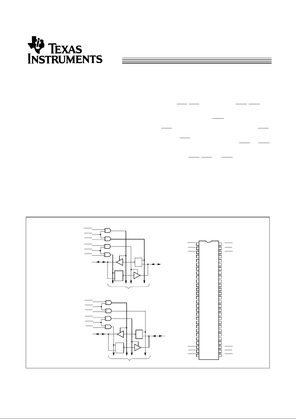
Logic Block Diagrams PinConfiguration
1
OEAB
SSOP/TSSOP
Top View
GND
V
CC
TO 7 OTHERCHANNELS
D
C
1
B
1
1
OEBA
1
A
1
1
CEBA
1
LEAB
1
OEAB
1
LEBA
1
CEAB
D
C
D
C
2
B
1
2
OEBA
2
A
1
2
CEBA
2
OEAB
2
LEBA
2
CEAB
1
LEAB
1
CEAB
1
A
1
V
CC
GND
2
LEAB
1
A
2
1
A
3
1
A
5
1
A
4
1
A
6
1
A
7
1
A
8
GND
2
A
1
2
A
2
2
A
3
2
A
4
2
A
5
2
A
6
2
A
7
2
A
8
GND
2
OEAB
2
CEAB
2
LEAB
1
2
3
4
5
6
7
8
9
10
11
12
13
14
15
16
17
18
19
20
21
22
23
24
25
26
27
28
56
55
54
53
52
51
50
49
48
47
46
45
44
43
42
41
40
39
38
37
36
35
34
33
32
31
30
29
1
OEBA
GND
V
CC
1
LEBA
1
CEBA
1
B
1
V
CC
GND
1
B
2
1
B
3
1
B
5
1
B
4
1
B
6
1
B
7
1
B
8
GND
2
B
1
2
B
2
2
B
3
2
B
4
2
B
6
2
B
7
2
B
8
GND
2
OEBA
2
CEBA
2
LEBA
2
B
5
D
C
TO 7 OTHER CHANNELS
CY74FCT163543
2
Maximum Ratings
[3, 4]
(Above which the useful life may be impaired. For user
guidelines, not tested.)
Storage Temperature .............................. −55°C to +125°C
Ambient Temperature with
Power Applied.......................................... −55°C to +125°C
Supply Voltage Range ..................................... 0.5V to +4.6V
DC Input Voltage .................................................−0.5V to +7.0V
DC Output Voltage..............................................−0.5V to +7.0V
DC Output Current
(Maximum Sink Current/Pin)...........................−60 to +120 mA
Power Dissipation..........................................................1.0W
Static Discharge Voltage............................................>2001V
(per MIL-STD-883, Method 3015)
Pin Description
Name Description
OEAB A-to-B Output Enable Input (Active LOW)
OEBA B-to-A Output Enable Input (Active LOW)
CEAB A-to-B Enable Input (Active LOW)
CEBA B-to-A Enable Input (Active LOW)
LEAB A-to-B Latch Enable Input (Active LOW)
LEBA B-to-A Latch Enable Input (Active LOW)
A A-to-B Data Inputs or B-to-A Three-State Outputs
B B-to-A Data Inputs or A-to-B Three-State Outputs
Function Table
[1]
Inputs
Latch
Status
Output
Buffers
CEAB LEAB OEAB A to B B
H X X Storing High Z
X H X Storing X
X X H X High Z
L L L Transparent Current A
Inputs
L H L Storing Previous A
Inputs
[2]
Operating Range
Range
Ambient
Temperature V
CC
Industrial −40°C to +85°C 2.7V to 3.6V
CY74FCT163543
3
Electrical Characteristics Over the Operating Range V
CC
=2.7V to 3.6V
Parameter Description Test Conditions Min. Typ.
[5]
Max. Unit
V
IH
Input HIGH Voltage 2.0 5.5 V
V
IL
Input LOW Voltage 0.8 V
V
H
Input Hysteresis
[6]
100 mV
V
IK
Input Clamp Diode Voltage V
CC
=Min., I
IN
=−18 mA −0.7 −1.2 V
I
IH
Input HIGH Current V
CC
=Max., V
CC
=5.5V +1 µA
I
IL
Input LOW Current V
CC
=Max., V
CC
=GND +1 µA
I
OZH
High Impedance Output Current
(Three-State pins)
V
CC
=Max., V
OUT
=5.5V +1 µA
I
OZL
High Impedance Output Current
(Three-State pins)
V
CC
=Max., V
OUT
=GND +1 µA
I
ODL
Output LOW Current
[7]
V
CC
=3.3V,
V
OUT
=1.5V
V
IN
=V
IH
or V
IL
, 50 90 200 mA
I
ODH
Output HIGH Current
[7]
V
CC
=3.3V,
V
OUT
=1.5V
V
IN
=V
IH
or V
IL
, −36 −60 −110 mA
V
OH
Output HIGH Voltage V
CC
=Min., I
OH
=−0.1 mA V
CC
−0.2 V
V
CC
=3.0V, I
OH
=−8 mA 2.4 3.0
V
CC
=3.0V, I
OH
=−24 mA 2.0 3.0
V
OL
Output LOW Voltage V
CC
=Min., I
OL
=0.1mA 0.2 V
V
CC
=Min., I
OL
=24mA 3.0 0.5
I
OS
Short Circuit Current
[7]
V
CC
=Max., V
OUT
=GND −60 −135 −240 mA
I
OFF
Power-Off Disable V
CC
=0V, V
OUT
<4.5V +100 µA
Notes:
1. A-to-B data flow shown; B-to-A flow control is the same, except using
CEBA, LEBA, and OEBA.
2. Data prior to LEAB LOW-to-HIGH Transition H = HIGH Voltage Level. L = LOW Voltage Level. X = Don’t Care. Z = High Impedance.
3. Operation beyond the limits set forth may impair the useful life of the device. Unless noted, these limits are over the operating free-air temperature range.
4. Unused inputs must always be connected to an appropriate logic voltage level, preferably either V
CC
or ground.
5. Typical values are at V
CC
= 3.3V, T
A
= +25˚C ambient.
6. This parameter is specified but not tested.
7. Not more than one output should be shortedat a time. Duration of short should not exceed one second. The use of high-speed test apparatus and/or sample
and hold techniques are preferable in order to minimize internal chip heating and more accurately reflect operational values. Otherwise prolonged shorting
of a high output may raise the chip temperature well abovenormal and thereby cause invalidreadings in other parametric tests. In any sequence of parameter
tests, I
OS
tests should be performed last.
Capacitance
[6]
(T
A
= +25˚C, f = 1.0 MHz)
Parameter Description Test Conditions Typ.
[5]
Max. Unit
C
IN
Input Capacitance V
IN
= 0V 4.5 6.0 pF
C
OUT
Output Capacitance V
OUT
= 0V 5.5 8.0 pF
 Loading...