


CD74HCT597M96
Texas Instruments CD74HCT597M96, CD74HCT597M, CD74HCT597E, CD74HC597M96, CD74HC597M Datasheet
...
1
Data sheet acquired from Harris Semiconductor
SCHS191
Features
• Buffered Inputs
• Asynchronous Parallel Load
• Typical f
MAX
= 60MHz at V
CC
=5V,C
L
= 15pF, T
A
=25
o
C
• Fanout (Over Temperature Range)
- Standard Outputs. . . . . . . . . . . . . . . 10 LSTTL Loads
- Bus Driver Outputs . . . . . . . . . . . . . 15 LSTTL Loads
• Wide Operating Temperature Range . . . -55
o
C to 125
o
C
• Balanced Propagation Delay and Transition Times
• Significant Power Reduction Compared to LSTTL
Logic ICs
• HC Types
- 2V to 6V Operation
- High Noise Immunity: N
IL
= 30%, N
IH
= 30% of V
CC
at V
CC
= 5V
• HCT Types
- 4.5V to 5.5V Operation
- Direct LSTTL Input Logic Compatibility,
V
IL
= 0.8V (Max), V
IH
= 2V (Min)
- CMOS Input Compatibility, I
l
≤ 1µA at V
OL
, V
OH
Description
The Harris CD74HC597 and CD74HCT597 are high-speed
silicon gate CMOS devices that are pin-compatible with the
LSTTL 597 devices. Each device consists of an 8-flip-flop
input register and an 8-bit parallel-in/serial-in, serial-out shift
register.Each register is controlled by its own clock. A “low”on
the parallel load input (
PL) shifts parallel stored data asyn-
chronously into the shift register. A “low” master input (
MR)
clears the shift register. Serial input data can also be synchro-
nously shifted through the shift register when
PL is high.
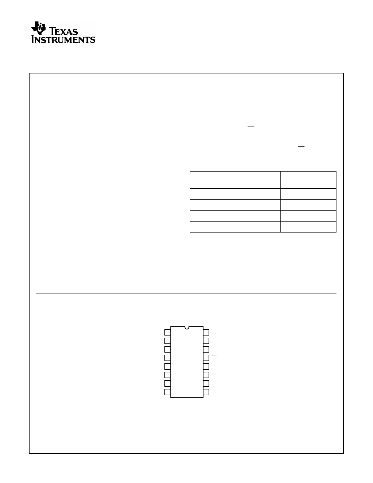
Pinout
CD74HC597, CD74HCT597
(PDIP, SOIC)
TOP VIEW
Ordering Information
PART NUMBER TEMP. RANGE (
o
C) PACKAGE
PKG.
NO.
CD74HC597E -55 to 125 16 Ld PDIP E16.3
CD74HCT597E -55 to 125 16 Ld PDIP E16.3
CD74HC597M -55 to 125 16 Ld SOIC M16.15
CD74HCT597M -55 to 125 16 Ld SOIC M16.15
NOTES:
1. When ordering, use the entire part number.Add the suffix 96 to
obtain the variant in the tape and reel.
2. Wafer and die is available which meets all electrical
specifications. Please contact your local sales office or Harris
customer service for ordering information.
14
15
16
9
13
12
11
10
1
2
3
4
5
7
6
8
D1
D2
D3
D4
D5
D6
GND
D7
V
CC
D
S
PL
ST
CP
SH
CP
MR
Q7
D0
January 1998
CAUTION: These devices are sensitive to electrostatic discharge. Users should follow proper IC Handling Procedures.
Copyright
© Harris Corporation 1998
File Number 1915.1
CD74HC597,
CD74HCT597
High Speed CMOS Logic
8-Bit Shift Register with Input Storage
[ /Title
(CD74
HC597
,
CD74
HCT59
7)
/
Sub-
j
ect
(High
Speed
CMOS
2
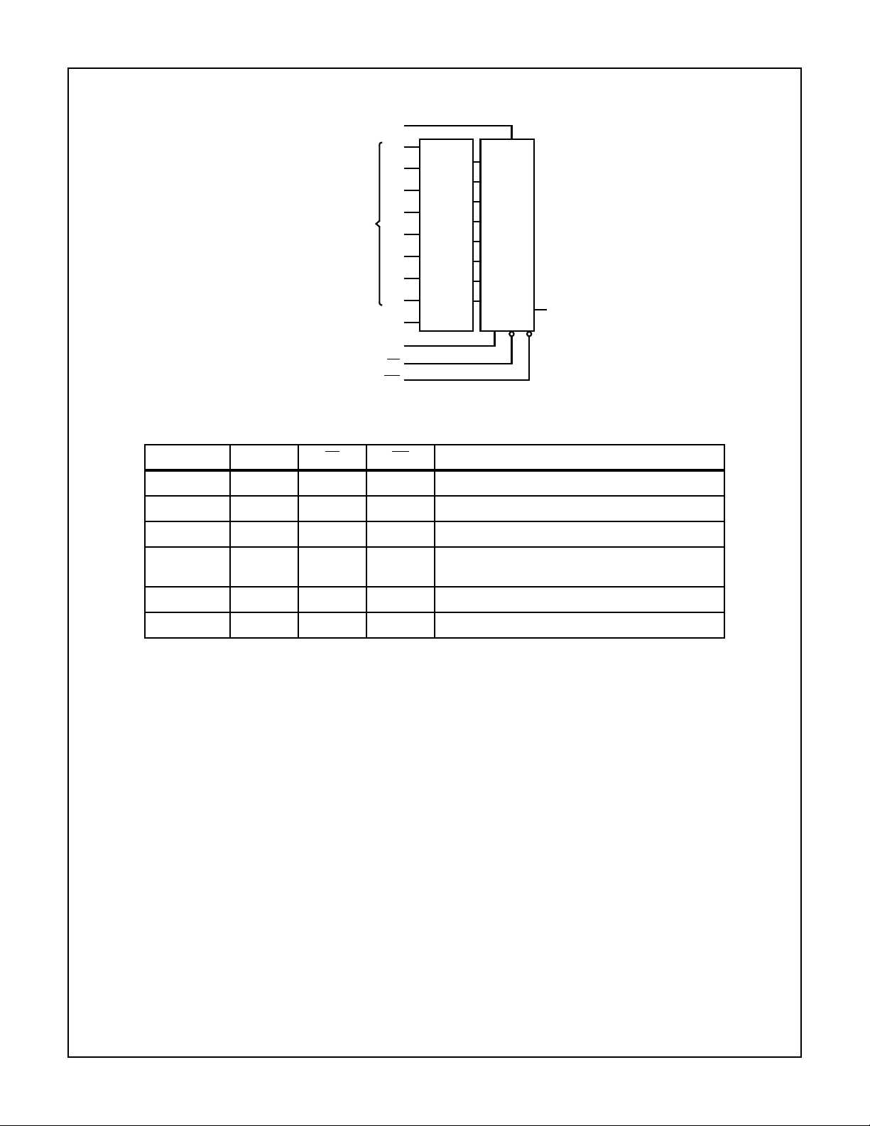
Functional Diagram
9
1
2
3
4
6
12
7
5
D1
D2
D3
D4
D5
D6
D7
ST
CP
Q7
11
13
10
15
14
D0
DS
SH
CP
PL
MR
8 F/F
STORAGE
REG.
8-BIT
SHIFT
REG.
PARALLEL
DAT A
INPUTS
FUNCTION TABLE
ST
CP
SH
CP
PL MR FUNCTION
↑ X X X Data Loaded to Input Flip-Flops
↑ X L H Data Loaded from Inputs to Shift Register
No Clock Edge X L H Data Transferred from Input Flip-Flops to Shift Register
X X L L InvalidLogic, State of Shift Register Indeterminate when
Signals Removed
X X H L Shift Register Cleared
X ↑ H H Shift Register Clocked Qn = Qn-1, Q0 = D
S
NOTE: H = High Voltage Level, L = Low Voltage Level, X = Don’t Care,↑ = Transition from Low to High CP Level
CD74HC597, CD74HCT597
3
Absolute Maximum Ratings Thermal Information
DC Supply Voltage, V
CC
. . . . . . . . . . . . . . . . . . . . . . . . -0.5V to 7V
DC Input Diode Current, I
IK
For V
I
< -0.5V or V
I
> V
CC
+ 0.5V. . . . . . . . . . . . . . . . . . . . . .±20mA
DC Output Diode Current, I
OK
For V
O
< -0.5V or V
O
> V
CC
+ 0.5V . . . . . . . . . . . . . . . . . . . .±20mA
DC Drain Current, per Output, I
O
For -0.5V < V
O
< V
CC
+ 0.5V. . . . . . . . . . . . . . . . . . . . . . . . . .±25mA
DC Output Source or Sink Current per Output Pin, I
O
For V
O
> -0.5V or V
O
< V
CC
+ 0.5V . . . . . . . . . . . . . . . . . . . .±25mA
DC V
CC
or Ground Current, I
CC
. . . . . . . . . . . . . . . . . . . . . . . . .±50mA
Operating Conditions
Temperature Range, T
A
. . . . . . . . . . . . . . . . . . . . . . -55
o
C to 125
o
C
Supply Voltage Range, V
CC
HC Types . . . . . . . . . . . . . . . . . . . . . . . . . . . . . . . . . . . . .2V to 6V
DC Input or Output Voltage, V
I
, V
O
. . . . . . . . . . . . . . . . . 0V to V
CC
Input Rise and Fall Time
2V . . . . . . . . . . . . . . . . . . . . . . . . . . . . . . . . . . . . . . 1000ns (Max)
4.5V. . . . . . . . . . . . . . . . . . . . . . . . . . . . . . . . . . . . . . 500ns (Max)
6V . . . . . . . . . . . . . . . . . . . . . . . . . . . . . . . . . . . . . . . 400ns (Max)
Thermal Resistance (Typical, Note 3) θ
JA
(
o
C/W)
PDIP Package. . . . . . . . . . . . . . . . . . . . . . . . . . . . . 90
SOIC Package. . . . . . . . . . . . . . . . . . . . . . . . . . . . . 160
Maximum Junction Temperature. . . . . . . . . . . . . . . . . . . . . . . 150
o
C
Maximum Storage Temperature Range . . . . . . . . . .-65
o
C to 150
o
C
Maximum Lead Temperature (Soldering 10s). . . . . . . . . . . . . 300
o
C
(SOIC - Lead Tips Only)
CAUTION: Stresses above those listed in “Absolute Maximum Ratings” may cause permanent damage to the device. This is a stress only rating and operation
of the device at these or any other conditions above those indicated in the operational sections of this specification is not implied.
NOTE:
3. θ
JA
is measured with the component mounted on an evaluation PC board in free air.
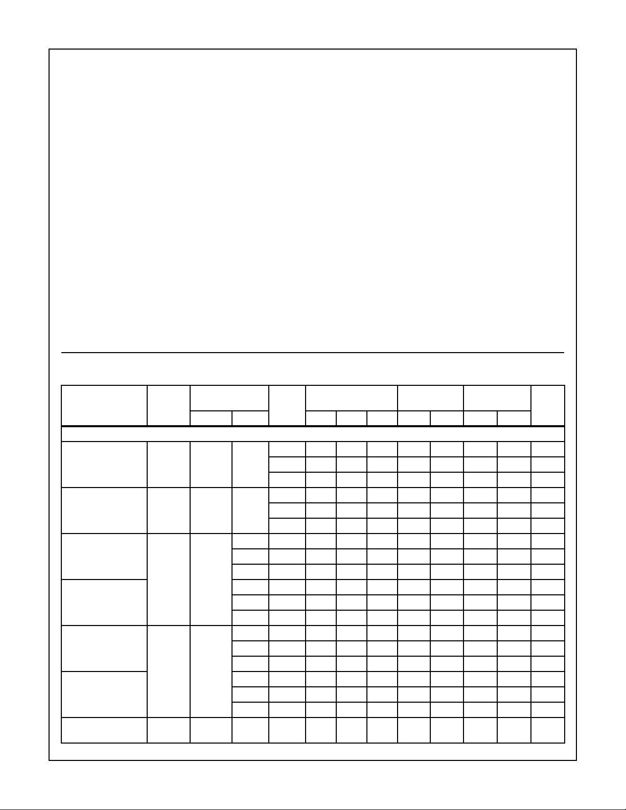
DC Electrical Specifications
PARAMETER SYMBOL
TEST
CONDITIONS
V
CC
(V)
25
o
C -40
o
C TO 85
o
C -55
o
CTO125
o
C
UNITSV
I
(V) I
O
(mA) MIN TYP MAX MIN MAX MIN MAX
HC TYPES
High Level Input
Voltage
V
IH
- - 2 1.5 - - 1.5 - 1.5 - V
4.5 3.15 - - 3.15 - 3.15 - V
6 4.2 - - 4.2 - 4.2 - V
Low Level Input
Voltage
V
IL
- - 2 - - 0.5 - 0.5 - 0.5 V
4.5 - - 1.35 - 1.35 - 1.35 V
6 - - 1.8 - 1.8 - 1.8 V
High Level Output
Voltage
CMOS Loads
V
OH
V
IH
or V
IL
-0.02 2 1.9 - - 1.9 - 1.9 - V
-0.02 4.5 4.4 - - 4.4 - 4.4 - V
-0.02 6 5.9 - - 5.9 - 5.9 - V
High Level Output
Voltage
TTL Loads
- - ---- - - -V
-4 4.5 3.98 - - 3.84 - 3.7 - V
-5.2 6 5.48 - - 5.34 - 5.2 - V
Low Level Output
Voltage
CMOS Loads
V
OL
V
IH
or V
IL
0.02 2 - - 0.1 - 0.1 - 0.1 V
0.02 4.5 - - 0.1 - 0.1 - 0.1 V
0.02 6 - - 0.1 - 0.1 - 0.1 V
Low Level Output
Voltage
TTL Loads
- - ---- - - -V
4 4.5 - - 0.26 - 0.33 - 0.4 V
5.2 6 - - 0.26 - 0.33 - 0.4 V
Input Leakage
Current
I
I
V
CC
or
GND
-6--±0.1 - ±1-±1µA
CD74HC597, CD74HCT597
 Loading...