


CY74FCT2244CTQCT
Texas Instruments CY74FCT2244CTQCT, CY74FCT2244CTQC, CY74FCT2244ATSOCT, CY74FCT2244ATSOC, CY74FCT2244ATQCT Datasheet
...
8-Bit Buffers/Line Drivers
CY74FCT2240T
CY74FCT2244T
CCS036 - September 1994 - Revised March 2000
Data sheet acquired from Cypress Semiconductor Corporation.
Data sheet modified to remove devices not offered.
Copyright © 2000, Texas Instruments Incorporated
Features
• Function and pinout compatible with FCT and F logic
• 25Ωoutputseriesresistorstoreducetransmissionline
reflection noise
• FCT-C speed at 4.1 ns max. (Com’l) FCT-A speed at 4.8
ns max. (Com’l)
• TTL output level versions of equivalent FCT functions
• Edge-rate control circuitry for significantly improved
noise characteristics
• Power-off disable feature permits live insertion
• ESD > 2000V
• Fully compatible with TTL input and output logic levels
• Sink current 12 mA
Source current15 mA
• Extended commercial temp. range of –40˚C to +85˚C
• Three-state outputs
Functional Description
The FCT2240T and FCT2244T are octal buffers and line
drivers that include on-chip 25Ω terminating resistors at each
of the outputs, to minimize noise resulting from reflections or
standing wavesin high-performance applications.The on-chip
resistors reduce overall board space and component count.
Designed to be employed as memory address drivers, clock
drivers, and bus-oriented transmitters/receivers, these devic-
es provide speed and drive capabilities commensurate with
their fastest bipolar logic counterparts while reducing power
dissipation. The input and output voltage levels allow direct
interface with TTL, NMOS, and CMOS devices without the
need for external components.
The outputs are designed with a power-off disable feature to
allow for liv e insertion of boards.
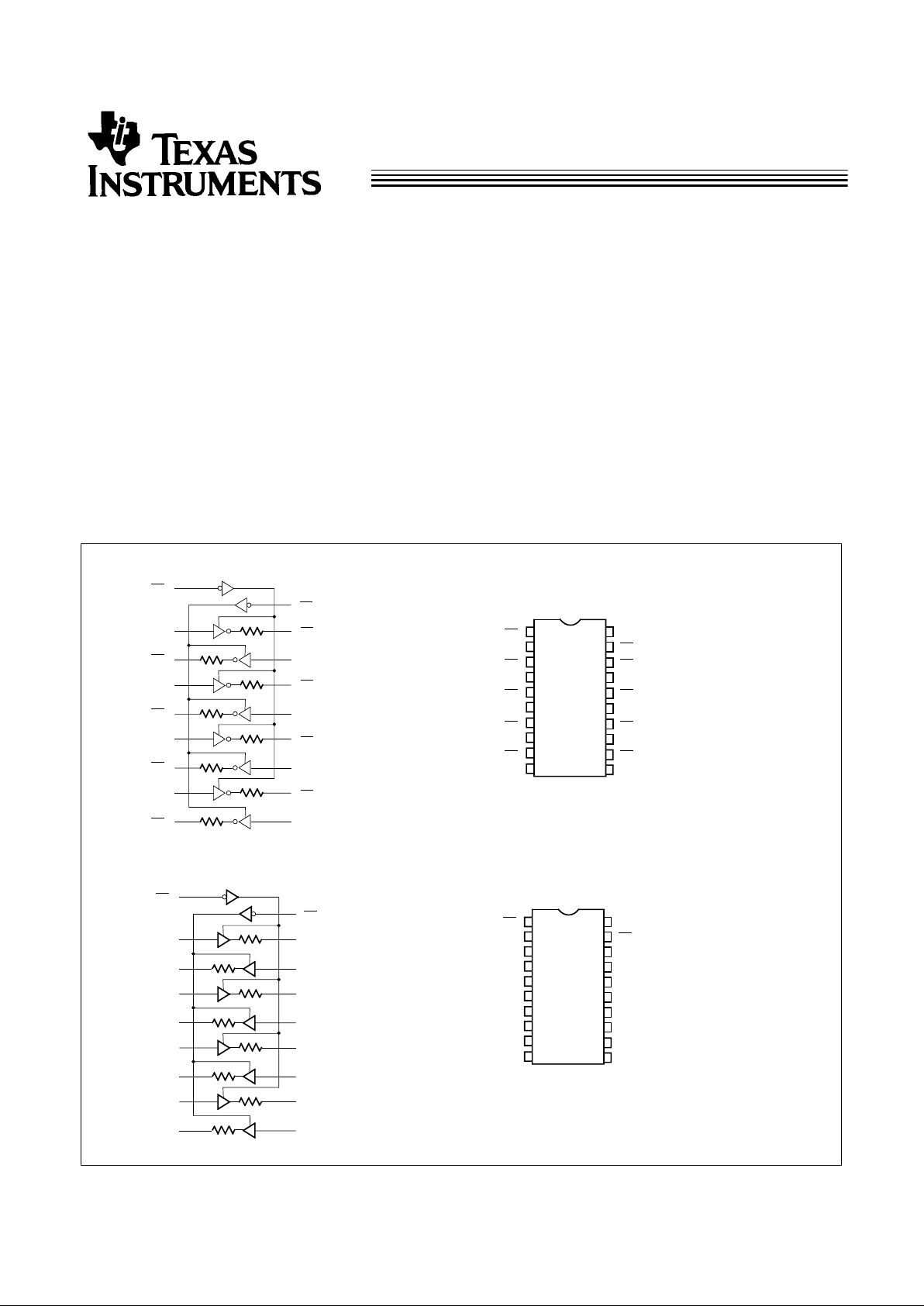
Logic Block Diagram FCT2240T Pin Configurations
FCT2240T–2
1
2
3
4
5
6
7
8
9
10 11
12
16
17
18
19
20
13
14
OE
A
DA
0
OB
0
DA
1
OB
1
DA
2
DA
3
GND
V
CC
FCT2240T
–3
15
SOIC/QSOP
Top View
OB
2
OB
3
OE
B
OA
0
OA
2
DB
2
DB
3
OA
3
DB
0
OA
1
DB
1
OE
B
OE
A
DA
0
OB
0
DA
1
OB
1
DA
2
DA
3
OB
2
OB
3
OA
0
OA
2
DB
2
DB
3
OA
3
DB
0
OA
1
DB
1
Logic Block Diagram FCT2244T
1
2
3
4
5
6
7
8
9
10 11
12
16
17
18
19
20
13
14
OE
A
DA
0
OB
0
DA
1
OB
1
DA
2
DA
3
GND
V
CC
15
DIP/SOIC/QSOP
Top View
OB
2
OB
3
OE
B
OA
0
OA
2
DB
2
DB
3
OA
3
DB
0
OA
1
DB
1
OE
B
OE
A
DA
0
OB
0
DA
1
OB
1
DA
2
DA
3
OB
2
OB
3
OA
0
OA
2
DB
2
DB
3
OA
3
DB
0
OA
1
DB
1
FCT2240T–4
FCT2240T–6
FCT2240T
FCT2244T
CY74FCT2240T
CY74FCT2244T
2
]
Maximum Ratings
[2, 3]
(Above which the useful life may be impaired. For user guide-
lines, not tested.)
Storage Temperature .................................–65°C to +150°C
Ambient Temperature with
Power Applied.............................................–65°C to +135°C
Supply Voltage to Ground Potential............... –0.5V to +7.0V
DC Input Voltage............................................–0.5V to +7.0V
DC Output Voltage......................................... –0.5V to +7.0V
DC Output Current (Maximum Sink Current/Pin) ......120 mA
Power Dissipation..........................................................0.5W
Static Discharge Voltage............................................>2001V
(per MIL-STD-883, Method 3015)
Function Table FCT2240T
[1]
Inputs
OutputOE
A
OE
B
D
L
L
H
L
L
H
L
H
X
H
L
Z
Function Table FCT2244T
[1]
Inputs
OutputOE
A
OE
B
D
L
L
H
L
L
H
L
H
X
L
H
Z
Operating Range
Range Range
Ambient
Temperature V
CC
Commercial T, AT, CT –40°C to +85°C 5V ± 5%
Electrical Characteristics Over the Operating Range
Parameter Description Test Conditions Min. Typ.
[5]
Max. Unit
V
OH
Output HIGH Voltage V
CC
=Min., I
OH
=–15 mA Com’l 2.4 3.3 V
V
OL
Output LOW Voltage V
CC
=Min., I
OL
=12 mA Com’l 0.3 0.55 V
R
OUT
Output Resistance V
CC
=Min., I
OL
=12 mA Com’l 20 25 40 Ω
V
IH
Input HIGH Voltage 2.0 V
V
IL
Input LOW Voltage 0.8 V
V
H
Hysteresis
[6]
All inputs 0.2 V
V
IK
Input Clamp Diode Voltage V
CC
=Min., I
IN
=–18 mA –0.7 –1.2 V
I
I
Input HIGH Current V
CC
=Max., V
IN
=V
CC
5 µA
I
IH
Input HIGH Current V
CC
=Max., V
IN
=2.7V ±1 µA
I
IL
Input LOW Current V
CC
=Max., V
IN
=0.5V ±1 µA
I
OZH
Off State HIGH-Level
Output Current
V
CC
=Max., V
OUT
=2.7V 10 µA
I
OZL
Off State LOW-Level
Output Current
V
CC
=Max., V
OUT
=0.5V –10 µA
I
OS
Output Short Circuit Current
[7]
V
CC
=Max., V
OUT
=0.0V –60 –120 –225 mA
I
OFF
Power-Off Disable V
CC
=0V, V
OUT
=4.5V ±1 µA
Notes:
1. H = HIGH Voltage Level. L = LOW Voltage Level. X = Don’t Care.
2. Unless otherwise noted, these limits are over the operating free-air temperature range.
3. Unused inputs must always be connected to an appropriate logic voltage level, preferably either V
CC
or ground.
4. T
A
is the “instant on” case temperature.
5. Typical values are at V
CC
=5.0V, T
A
=+25˚C ambient.
6. This parameter is specified but not tested.
7. Not more than one output should be shorted at a time. Duration of short should not exceedone second. The use of high-speed test apparatus and/or sample
and hold techniques are preferable in order to minimize internal chip heating and more accurately reflect operational values. Otherwise prolonged shorting of
a high output may raise the chip temperature well above normal and thereby cause invalid readings in other parametric tests. In any sequence of parameter
tests, I
OS
tests should be performed last.
 Loading...