


CD74HCT27M96
Texas Instruments CD74HCT27M96, CD74HCT27M, CD74HCT27E, CD74HC27M96, CD74HC27M Datasheet
...
CD74HC27,
/
j
[ /Title
(CD74
HC27,
CD74
HCT27
)
Sub-
ect
(High
Speed
CMOS
Logic
Data sheet acquired from Harris Semiconductor
SCHS132
August 1997
Features
• Buffered Inputs
• Typical Propagation Delay: 7ns at V
C
= 15pF, TA = 25oC
L
• Fanout (Over Temperature Range)
- Standard Outputs. . . . . . . . . . . . . . . 10 LSTTL Loads
- Bus Driver Outputs . . . . . . . . . . . . . 15 LSTTL Loads
• Wide Operating Temperature Range . . . -55
• Balanced Propagation Delay and Transition Times
• Significant Power Reduction Compared to LSTTL
Logic ICs
• HC Types
- 2V to 6V Operation
- High Noise Immunity: N
at VCC = 5V
• HCT Types
- 4.5V to 5.5V Operation
- Direct LSTTL Input Logic Compatibility,
V
= 0.8V (Max), VIH = 2V (Min)
IL
- CMOS Input Compatibility, I
= 30%, NIH = 30% of V
IL
≤ 1µA at VOL, V
l
CC
= 5V,
o
C to 125oC
CC
OH
CD74HCT27
High Speed CMOS Logic
Triple 3-Input NOR Gate
Description
The Harris CD74HC27, CD74HCT27, logic gates utilize
silicon gate CMOS technology to achieve operating speeds
similar to LSTTL gates with the low power consumption of
standard CMOS integrated circuits. All devices have the
ability to drive 10 LSTTL loads. The 74HCT logic family is
functionally pin compatible with the standard 74LS logic
family.
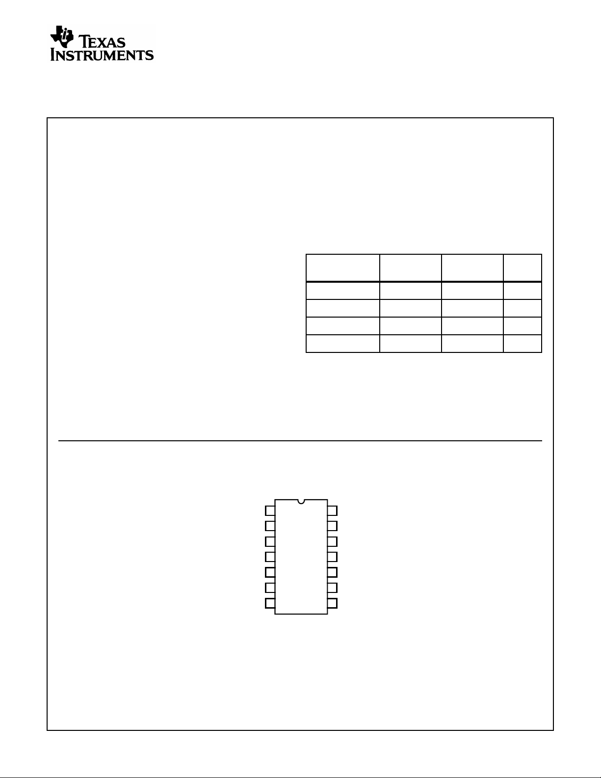
Ordering Information
TEMP.RANGE
PART NUMBER
CD74HC27E -55 to 125 14 Ld PDIP E14.3
CD74HCT27E -55 to 125 14 Ld PDIP E14.3
CD74HC27M -55 to 125 14 Ld SOIC M14.15
CD74HCT27M -55 to 125 14 Ld SOIC M14.15
NOTES:
1. When ordering, use the entire part number.Add the suffix 96 to
obtain the variant in the tape and reel.
2. Die for this part number is available which meets all electrical
specifications. Please contact your local sales office or Harris
customer service for ordering information.
(oC) PACKAGE
PKG.
NO.
Pinout
CD74HC27, CD74HCT27
(PDIP, SOIC)
TOP VIEW
1A
1
2
1B
3
2A
4
2B
5
2C
6
2Y
7
GND
14
V
CC
1C
13
12
1Y
3C
11
3B
10
3A
9
3Y
8
CAUTION: These devices are sensitive to electrostatic discharge. Users should follow proper IC Handling Procedures.
Copyright
© Harris Corporation 1997
1
File Number 1648.1
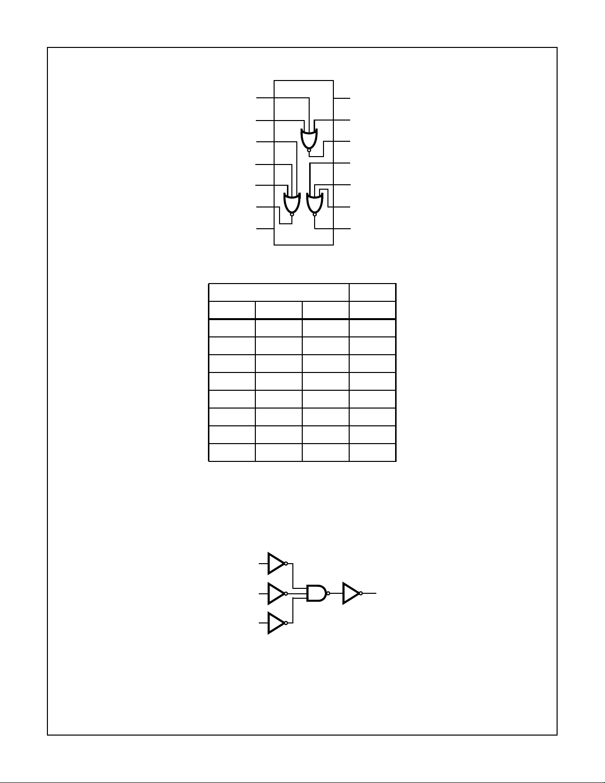
Functional Diagram
CD74HC27, CD74HCT27
1A
1B
2A
2B
2C
2Y
GND
1
2
3
4
5
6
7
14
V
CC
13
1C
12
1Y
11
3C
10
3B
9
3A
8
3Y
TRUTH TABLE
INPUTS OUTPUT
nA nB nC nY
LLLH
LLHL
LHLL
Logic Symbol
HLLL
HHLL
LHHL
HLHL
HHHL
NOTE: H = High Voltage Level,L = Low Voltage Level
nA
nB
nC
nY
2
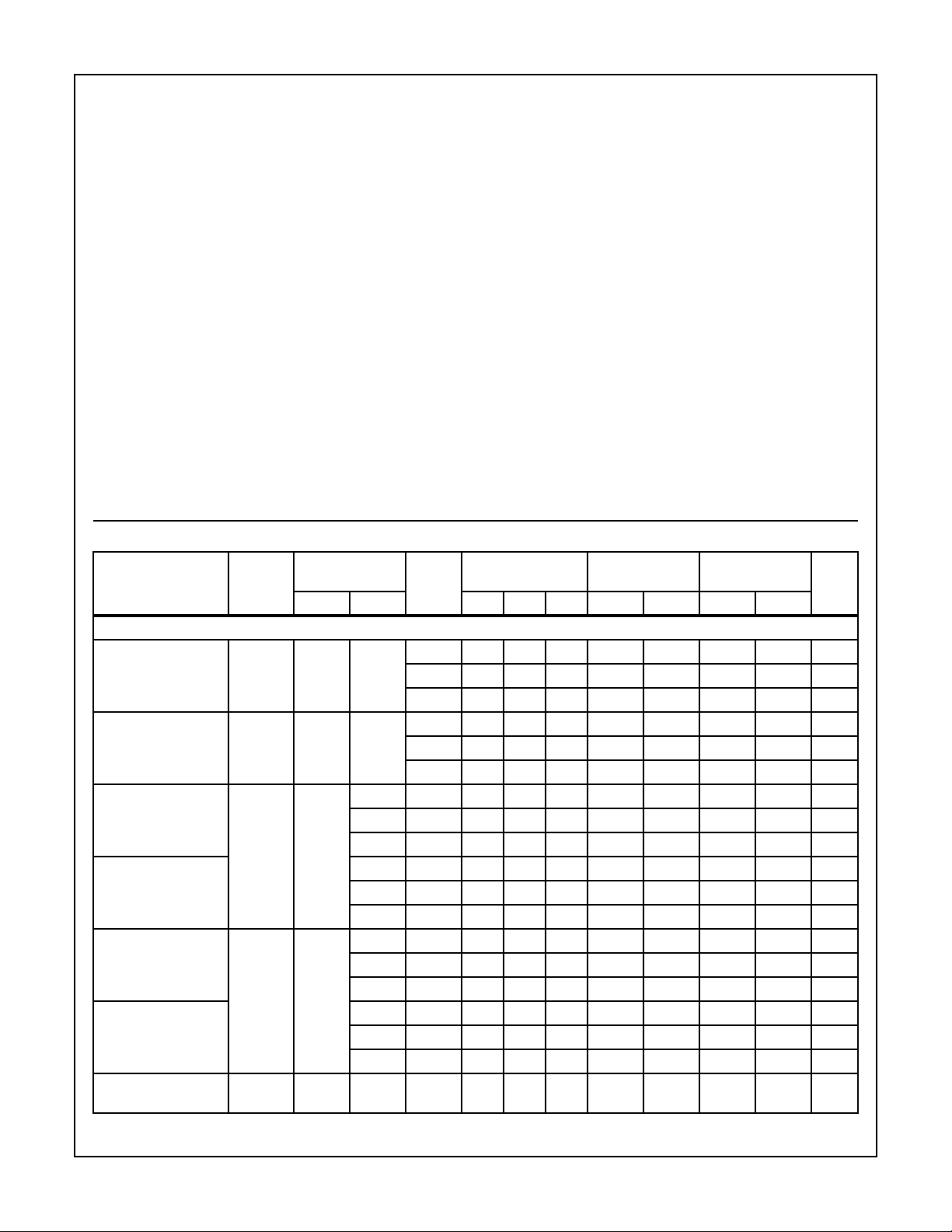
CD74HC27, CD74HCT27
Absolute Maximum Ratings Thermal Information
DC Supply Voltage, VCC. . . . . . . . . . . . . . . . . . . . . . . . -0.5V to 7V
DC Input Diode Current, I
IK
For VI < -0.5V or VI > VCC + 0.5V. . . . . . . . . . . . . . . . . . . . . .±20mA
DC Output Diode Current, I
OK
For VO < -0.5V or VO > VCC + 0.5V . . . . . . . . . . . . . . . . . . . .±20mA
DC Output Source or Sink Current per Output Pin, I
O
For VO > -0.5V or VO < VCC + 0.5V . . . . . . . . . . . . . . . . . . . .±25mA
DC VCC or Ground Current, I
CC orIGND
. . . . . . . . . . . . . . . . . .±50mA
Operating Conditions
Temperature Range (TA) . . . . . . . . . . . . . . . . . . . . . -55oC to 125oC
Supply Voltage Range, V
HC Types . . . . . . . . . . . . . . . . . . . . . . . . . . . . . . . . . . . . .2V to 6V
HCT Types . . . . . . . . . . . . . . . . . . . . . . . . . . . . . . . . .4.5V to 5.5V
DC Input or Output Voltage, VI, VO . . . . . . . . . . . . . . . . . 0V to V
Input Rise and Fall Time
2V . . . . . . . . . . . . . . . . . . . . . . . . . . . . . . . . . . . . . . 1000ns (Max)
4.5V. . . . . . . . . . . . . . . . . . . . . . . . . . . . . . . . . . . . . . 500ns (Max)
6V . . . . . . . . . . . . . . . . . . . . . . . . . . . . . . . . . . . . . . . 400ns (Max)
CAUTION: Stresses above those listed in “Absolute Maximum Ratings” may cause permanent damage to the device. This is a stress only rating and operation
of the device at these or any other conditions above those indicated in the operational sections of this specification is not implied.
NOTE:
3. θJA is measured with the component mounted on an evaluation PC board in free air.
CC
Thermal Resistance (Typical, Note 3) θJA (oC/W)
PDIP Package. . . . . . . . . . . . . . . . . . . . . . . . . . . . . 100
SOIC Package. . . . . . . . . . . . . . . . . . . . . . . . . . . . . 180
Maximum Junction Temperature. . . . . . . . . . . . . . . . . . . . . . .150oC
Maximum Storage Temperature Range . . . . . . . . . .-65oC to 150oC
Maximum Lead Temperature (Soldering 10s). . . . . . . . . . . . .300oC
(SOIC - Lead Tips Only)
CC
DC Electrical Specifications
PARAMETER SYMBOL
HC TYPES
High Level Input
Voltage
Low Level Input
Voltage
High Level Output
Voltage
CMOS Loads
High Level Output
Voltage
TTL Loads
Low Level Output
Voltage
CMOS Loads
Low Level Output
Voltage
TTL Loads
Input Leakage
Current
V
IH
V
IL
V
OH
V
OL
I
I
TEST
CONDITIONS
25oC -40oC TO 85oC -55oC TO 125oC
VCC (V)
- - 2 1.5 - - 1.5 - 1.5 - V
4.5 3.15 - - 3.15 - 3.15 - V
6 4.2 - - 4.2 - 4.2 - V
- - 2 - - 0.5 - 0.5 - 0.5 V
4.5 - - 1.35 - 1.35 - 1.35 V
6 - - 1.8 - 1.8 - 1.8 V
VIH or
V
-0.02 2 1.9 - - 1.9 - 1.9 - V
IL
-0.02 4.5 4.4 - - 4.4 - 4.4 - V
-0.02 6 5.9 - - 5.9 - 5.9 - V
---------V
-4 4.5 3.98 - - 3.84 - 3.7 - V
-5.2 6 5.48 - - 5.34 - 5.2 - V
VIH or
V
0.02 2 - - 0.1 - 0.1 - 0.1 V
IL
0.02 4.5 - - 0.1 - 0.1 - 0.1 V
0.02 6 - - 0.1 - 0.1 - 0.1 V
---------V
4 4.5 - - 0.26 - 0.33 - 0.4 V
5.2 6 - - 0.26 - 0.33 - 0.4 V
VCC or
-6--±0.1 - ±1-±1 µA
GND
UNITSVI(V) IO(mA) MIN TYP MAX MIN MAX MIN MAX
3
 Loading...