


CY74FCT257TQCT
Texas Instruments CY74FCT257TQCT, CY74FCT257TQC, CY74FCT257CTSOCT, CY74FCT257CTSOC, CY74FCT257CTQCT Datasheet
...
Quad 2-Input Multiplexe
r
CY74FCT257T
SCCS019 - May 1994 - Revised February 2000
Data sheet acquired from Cypress Semiconductor Corporation.
Data sheet modified to remove devices not offered.
Copyright © 2000, Texas Instruments Incorporated
Features
• Function, pinout, and drive compatible with FCT and
F logic
• FCT-C speed at 4.3 ns max.
FCT-A speed at 5.0 ns max.
• Reduced V
OH
(typically = 3.3V) versions of equivalent
FCT functions
• Edge-rate control circuitry for significantly improved
noise characteristics
• Power-off disable feature
• Matched rise and fall times
• Fully compatible with TTL input and output logic levels
• ESD > 2000V
• Extended commercial range of −40˚C to +85˚C
• Sink current 64 mA
Source current 32 mA
Functional Description
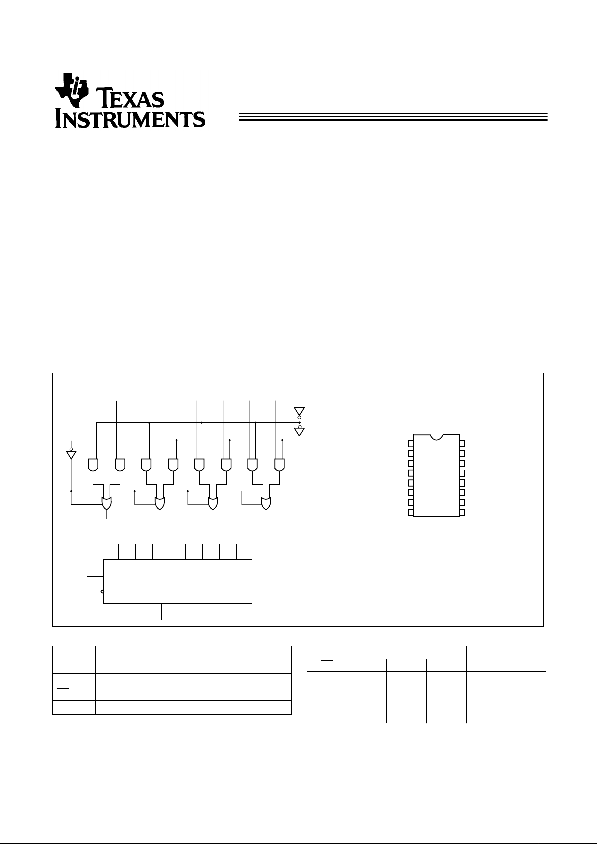
The FCT257T has four identical two-input multiplexers which
select four bits of data from two sources under the control of a
commondataSelectinput(S).The I
0
inputsareselectedwhen
the Select input is LOW and the I
1
inputs are selected when
the Select input is HIGH. Data appears at the output in true
non-inverted form for the FCT257T.
The FCT257T is a logic implementation of a four-pole, two
position switch where the position of the switch is determined
by the logic levels supplied to the select input. Outputs are
forced to a high-impedance “OFF” state when the Output
Enable input (
OE) is HIGH.
All but one device must be in the high-impedance state to
avoid currents exceeding the maximum ratings if outputs are
tiedtogether.Design of theOutputEnablesignals must ensure
that there is no overlap when outputs of three-state devices
are tied together.
The outputs are designed with a power-off disable feature to
allow for liv e insertion of boards.
Logic Block Diagram Pin Configurations
I
0a
SI
1a
I
0b
I
1b
I
0c
I
1c
I
0d
I
1d
Y
a
Y
b
Y
c
Y
d
OE
1
2
3
4
5
6
7
8
V
CC
GND
Top View
SOIC/QSOP
16
15
14
13
12
11
10
9
Y
a
S
I
1a
I
0a
I
1c
I
0c
OE
Y
b
I
1b
I
0b
I
1d
I
0d
Y
c
Y
d
Y
a
S
I
1a
I
0a
I
1d
I
0d
Y
b
I
1b
I
0b
I
1c
I
0c
Y
c
Y
d
OE
LogicSymbol
Pin Description
Name Description
I Data Inputs
S Common Select Input
OE Enable Inputs (Active LOW)
Y Data Outputs
Function Table
[1]
Inputs Outputs
OE S I
0
I
1
Y
H
L
L
L
L
X
H
H
L
L
X
X
X
L
H
X
L
H
X
X
H
L
H
L
H
Note:
1. H = HIGH Voltage Level, L = LOW Voltage Level, X = Don’t Care,
Z = High impedance (OFF) state.
CY74FCT257T
2
Maximum Ratings
[2,3]
(Above which the useful life may be impaired. For user
guidelines, not tested.)
Storage Temperature .....................................−65°C to +150°C
Ambient Temperature with
Power Applied..................................................−65°C to +135°C
Supply Voltage to Ground Potential..................−0.5V to +7.0V
DC Input Voltage .................................................−0.5V to +7.0V
DC Output Voltage ..............................................−0.5V to +7.0V
DC Output Current (Maximum Sink Current/Pin) ......120 mA
Power Dissipation..........................................................0.5W
Static Discharge Voltage............................................>2001V
(per MIL-STD-883, Method 3015)
Operating Range
Range Range
Ambient
Temperature V
CC
Commercial All −40°C to +85°C 5V ± 5%
Electrical Characteristics Over the Operating Range
Parameter Description Test Conditions Min. Typ.
[4]
Max. Unit
V
OH
Output HIGH Voltage V
CC
=Min., I
OH
=−32 mA 2.0 V
V
OL
Output LOW Voltage V
CC
=Min., I
OL
=64 mA 0.3 0.55 V
V
IH
Input HIGH Voltage 2.0 V
V
IL
Input LOW Voltage 0.8 V
V
H
Hysteresis
[5]
All inputs 0.2 V
V
IK
Input Clamp Diode Voltage V
CC
=Min., I
IN
=−18 mA −0.7 −1.2 V
I
I
Input HIGH Current V
CC
=Max., V
IN
=V
CC
5 µA
I
IH
Input HIGH Current V
CC
=Max., V
IN
=2.7V ±1 µA
I
IL
Input LOW Current V
CC
=Max., V
IN
=0.5V ±1 µA
I
OZH
Off State HIGH-Level Output Current V
CC
= Max., V
OUT
= 2.7V 10 µA
I
OZL
Off State LOW-Level
Output Current
V
CC
= Max., V
OUT
= 0.5V −10 µA
I
OS
Output Short Circuit Current
[6]
V
CC
=Max., V
OUT
=0.0V −60 −120 −225 mA
I
OFF
Power-Off Disable V
CC
=0V, V
OUT
=4.5V ±1 µA
Capacitance
[5]
Parameter Description Typ.
[4]
Max. Unit
C
IN
Input Capacitance 5 10 pF
C
OUT
Output Capacitance 9 12 pF
Notes:
2. Unless otherwise noted, these limits are over the operating free-air temperature range.
3. Unused inputs must always be connected to an appropriate logic voltage level, preferably either V
CC
or ground.
4. Typical values are at V
CC
=5.0V, T
A
=+25˚C ambient.
5. This parameter is specified but not tested.
6. Not morethanone output should beshorted ata time. Duration ofshort should notexceed one second. Theuse of high-speed test apparatusand/or sample
and holdtechniques are preferableinorder to minimize internalchipheating and more accuratelyreflect operational values.Otherwise prolonged shorting of
a high output mayraise the chip temperature well above normal and therebycauseinvalid readings in other parametric tests. In anysequence of parameter
tests, I
OS
tests should be performed last.
 Loading...