


Texas Instruments CD74HCT368M96, CD74HCT368M, CD74HCT368E, CD74HCT367M96, CD74HCT367M Datasheet
...Data sheet acquired from Harris Semiconductor SCHS181
November 1997
CD74HC367, CD74HCT367, CD74HC368, CD74HCT368
High Speed CMOS Logic Hex Buffer/Line Driver, Three-State Non-Inverting and Inverting
|
Features |
|
|
|
|
Description |
|
|
|
|
|
|||
|
• |
Buffered Inputs |
|
|
|
|
The Harris CD74HC367, CD74HCT367, CD74HC368, and |
|||||||
[ /Title |
• High Current Bus Driver Outputs |
|
|
CD74HCT368 silicon gate CMOS three-state buffers are gen- |
||||||||||
|
|
eral purpose high-speed non-inverting and inverting buffers. |
||||||||||||
(CD74 |
• Two Independent Three-State Enable Controls |
They have high drive current outputs which enable high speed |
||||||||||||
HC367 |
• |
Typical Propagation Delay t |
, t |
PHL |
= 8ns at V |
= 5V, |
operation even when driving large bus capacitances. These cir- |
|||||||
, |
|
C |
PLH |
|
CC |
cuits possess the low power dissipation of CMOS circuitry, yet |
||||||||
|
= 15pF, T = 25oC |
|
|
|
|
have speeds comparable to low power Schottky TTL circuits. |
||||||||
CD74 |
|
L |
A |
|
|
|
|
|||||||
• Fanout (Over Temperature Range) |
|
|
Both circuits are capable of driving up to 15 low power Schottky |
|||||||||||
HCT36 |
|
|
||||||||||||
|
- Standard Outputs . . . . . . . . . . . . . . . 10 LSTTL Loads |
inputs. |
|
|
|
|
|
|||||||
7, |
|
- Bus Driver Outputs . . . . . . . . . . . . . 15 LSTTL Loads |
The CD74HC367 and CD74HCT367 are non-inverting buffers, |
|||||||||||
CD74 |
• Wide Operating Temperature Range . . . -55oC to 125oC |
whereas the CD74HC368 and CD74HCT368 are inverting buff- |
||||||||||||
ers. These devices have two output enables, one enable (OE1) |
||||||||||||||
HC368 |
• |
Balanced Propagation Delay and Transition Times |
||||||||||||
, |
controls 4 gates and the other (OE2) controls the remaining 2 |
|||||||||||||
• Significant Power Reduction Compared to LSTTL |
gates. |
|
|
|
|
|
||||||||
CD74 |
|
|
|
|
|
|||||||||
The CD74HCT367 and CD74HCT368 logic families are speed, |
||||||||||||||
HCT36 |
|
Logic ICs |
|
|
|
|
||||||||
• HC Types |
|
|
|
|
function and pin compatible with the standard 74LS logic family. |
|||||||||
8) |
|
|
|
|
||||||||||
|
|
|
|
Ordering Information |
|
|
|
|||||||
/Sub- |
|
- 2V to 6V Operation |
|
|
|
|
|
|
|
|||||
|
|
|
|
|
|
|
|
|
|
|
||||
ject |
|
- High Noise Immunity: NIL = 30%, NIH = 30% of VCC |
|
TEMP. RANGE |
|
|
|
|
||||||
|
at VCC = 5V |
|
|
|
|
PART NUMBER |
(oC) |
|
PACKAGE |
|
PKG. NO. |
|||
(High |
|
|
|
|
|
|
|
|
|
|
|
|
|
|
• HCT Types |
|
|
|
|
CD74HC367E |
-55 to 125 |
|
16 Ld PDIP |
|
E16.3 |
||||
Speed |
|
|
|
|
|
|
||||||||
|
|
|
|
|
|
|
|
|
|
|||||
|
- 4.5V to 5.5V Operation |
|
|
|
|
CD74HCT367E |
-55 to 125 |
|
16 Ld PDIP |
|
E16.3 |
|||
|
|
|
|
|
|
|
|
|||||||
|
|
|
|
|
|
|
|
|
|
|
|
|||
|
|
- Direct LSTTL Input Logic Compatibility, |
|
CD74HCT368E |
-55 to 125 |
|
16 Ld PDIP |
|
E16.3 |
|||||
|
|
VIL= 0.8V (Max), VIH = 2V (Min) |
|
|
CD74HC367M |
-55 to 125 |
|
16 Ld SOIC |
|
M16.15 |
||||
|
|
- CMOS Input Compatibility, Il ≤ 1μA at VOL, VOH |
|
|
|
|
|
|
||||||
|
|
CD74HCT367M |
-55 to 125 |
|
16 Ld SOIC |
|
M16.15 |
|||||||
|
|
|
|
|
|
|
|
CD74HC368M |
-55 to 125 |
|
16 Ld SOIC |
|
M16.15 |
|
|
|
|
|
|
|
|
|
|
|
|
|
|
|
|
|
|
|
|
|
|
|
|
CD74HCT368M |
-55 to 125 |
|
16 Ld SOIC |
|
M16.15 |
|
|
|
|
|
|
|
|
|
|
|
|
|
|
|
|
|
|
|
|
|
|
|
|
NOTES: |
|
|
|
|
|
|
|
|
|
|
|
|
|
|
1. When ordering, use the entire part number. Add the suffix 96 to |
||||||
|
|
|
|
|
|
|
|
obtain the variant in the tape and reel. |
|
|||||
|
|
|
|
|
|
|
|
2. Wafer or die for this part number is available which meets all |
||||||
|
|
|
|
|
|
|
|
electrical specifications. Please contact your local sales office or |
||||||
|
|
|
|
|
|
|
|
Harris customer service for ordering information. |
|
|||||
|
|
|
|
|
|
|
|
|
|
|
|
|||
|
|
|
|
|
|
|
|
|
|
|
|
|||
|
|
|
|
|
|
|
|
|
|
|
|
|
|
|
|
Pinouts |
|
|
|
|
|
|
|
|
|
|
|||
|
|
|
CD74HC367, CD74HCT367 |
(PDIP, SOIC) |
|
CD74HC368, CD74HCT368 (PDIP, SOIC) |
|
|||||||
|
|
|
TOP VIEW |
|
|
|
|
TOP VIEW |
|
|
|
|||
OE1 |
1 |
16 VCC |
OE1 |
1 |
16 VCC |
1A |
2 |
15 OE2 |
1A |
2 |
15 OE2 |
1Y |
3 |
14 |
6A |
1Y |
3 |
14 |
6A |
2A |
4 |
13 |
6Y |
2A |
4 |
13 |
6Y |
2Y |
5 |
12 |
5A |
2Y |
5 |
12 |
5A |
3A |
6 |
11 |
5Y |
3A |
6 |
11 |
5Y |
3Y |
7 |
10 |
4A |
3Y |
7 |
10 |
4A |
GND |
8 |
9 |
4Y |
GND |
8 |
9 |
4Y |
CAUTION: These devices are sensitive to electrostatic discharge. Users should follow proper IC Handling Procedures. |
File Number 1538.1 |
|
Copyright © Harris Corporation 1997
1
CD74HC367, CD74HCT367, CD74HC368, CD74HCT368
Functional Diagrams
CD74HC367, CD74HCT367 |
||
1 |
16 |
|
OE1 |
VCC |
|
2 |
15 |
|
1A |
OE2 |
|
3 |
14 |
|
1Y |
6A |
|
4 |
13 |
|
2A |
6Y |
|
5 |
12 |
|
2Y |
5A |
|
6 |
11 |
|
3A |
||
5Y |
||
7 |
10 |
|
3Y |
4A |
|
8 |
9 |
|
GND |
4Y |
|
CD74HC368, CD74HCT368 |
||
1 |
16 |
|
OE1 |
VCC |
|
2 |
15 |
|
1A |
OE2 |
|
3 |
14 |
|
1Y |
6A |
|
4 |
13 |
|
2A |
6Y |
|
5 |
12 |
|
2Y |
5A |
|
6 |
11 |
|
3A |
||
5Y |
||
|
||
7 |
10 |
|
4A |
||
3Y |
||
8 |
9 |
|
GND |
4Y |
|
TRUTH TABLE
|
|
|
|
|
OUTPUTS |
||
|
|
INPUTS |
|
|
(Y) |
||
|
|
|
|
|
|
|
|
|
|
|
|
A |
HC/HCT367 |
|
HC/HCT368 |
|
OE |
||||||
|
|
|
|
|
|
|
|
|
L |
|
L |
L |
|
H |
|
|
|
|
|
|
|
|
|
|
L |
|
H |
H |
|
L |
|
|
|
|
|
|
|
|
|
|
H |
|
X |
(Z) |
|
(Z) |
|
|
|
|
|
|
|
|
|
NOTE:
H = High Voltage Level
L = Low Voltage Level
X = Don’t Care
Z = High Impedance (OFF) State
2

CD74HC367, CD74HCT367, CD74HC368, CD74HCT368
Logic Diagram
|
|
VCC |
|
|
|
16 |
|
|
ONE OF SIX IDENTICAL CIRCUITS |
|
|
|
2 |
|
|
1A |
|
|
|
|
(NOTE) |
3 |
|
|
1Y |
||
|
|
||
|
|
GND |
|
|
|
8 |
|
1 |
|
|
|
OE1 |
|
|
|
|
4 |
5 |
|
15 |
2A |
||
2Y |
|||
OE2 |
|
||
|
|
||
|
6 |
7 |
|
|
3A |
||
|
|
3Y |
|
|
10 |
9 |
|
|
4A |
||
|
4Y |
||
|
|
12
5A


 11
11
5Y
14
6A


 13
13
6Y
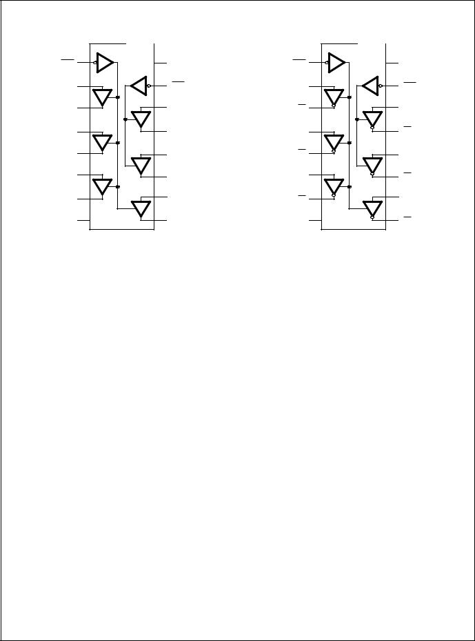
NOTE: Inverter not included in HC/HCT367.
FIGURE 1. LOGIC DIAGRAM FOR THE HC/HCT367 AND HC/HCT368 (OUTPUTS FOR HC/HCT367 ARE COMPLEMENTS OF THOSE SHOWN, i.e., 1Y, 2Y, ETC.)
3
 Loading...