


CY74FCT163827CPVCT
Texas Instruments CY74FCT163827CPVCT, CY74FCT163827CPVC, CY74FCT163827CPACT, CY74FCT163827CPAC, CY74FCT163827APVCT Datasheet
...
r
Data sheet acquired from Cypress Semiconductor Corporation.
Data sheet modified to remove devices not offered.
CY74FCT163827
SCCS049 - March 1997 - Revised March 2000
Features
• Low power, pin-compatible replacement for LCX and
LPT families
• 5V tolerant inputs and outputs
• 24 mA & 6 mA balanced drive outputs
• Power-off disable outputs permits live insertion
• Edge-rate control circuitry for reduced noise
• FCT-C speed at 4.1 ns
• Latch-up performance exceedsJEDEC standard no. 17
• Typical output skew < 250 ps
• Industrial temperature range of –40˚C to +85˚C
• TSSOP (19.6-mil pitch) or SSOP (25-mil pitch)
• Typical
Std 883D
•V
V
olp
= 2.7V to 3.6V
CC
(groundbounce)performanceexceedsMil
Functional Description
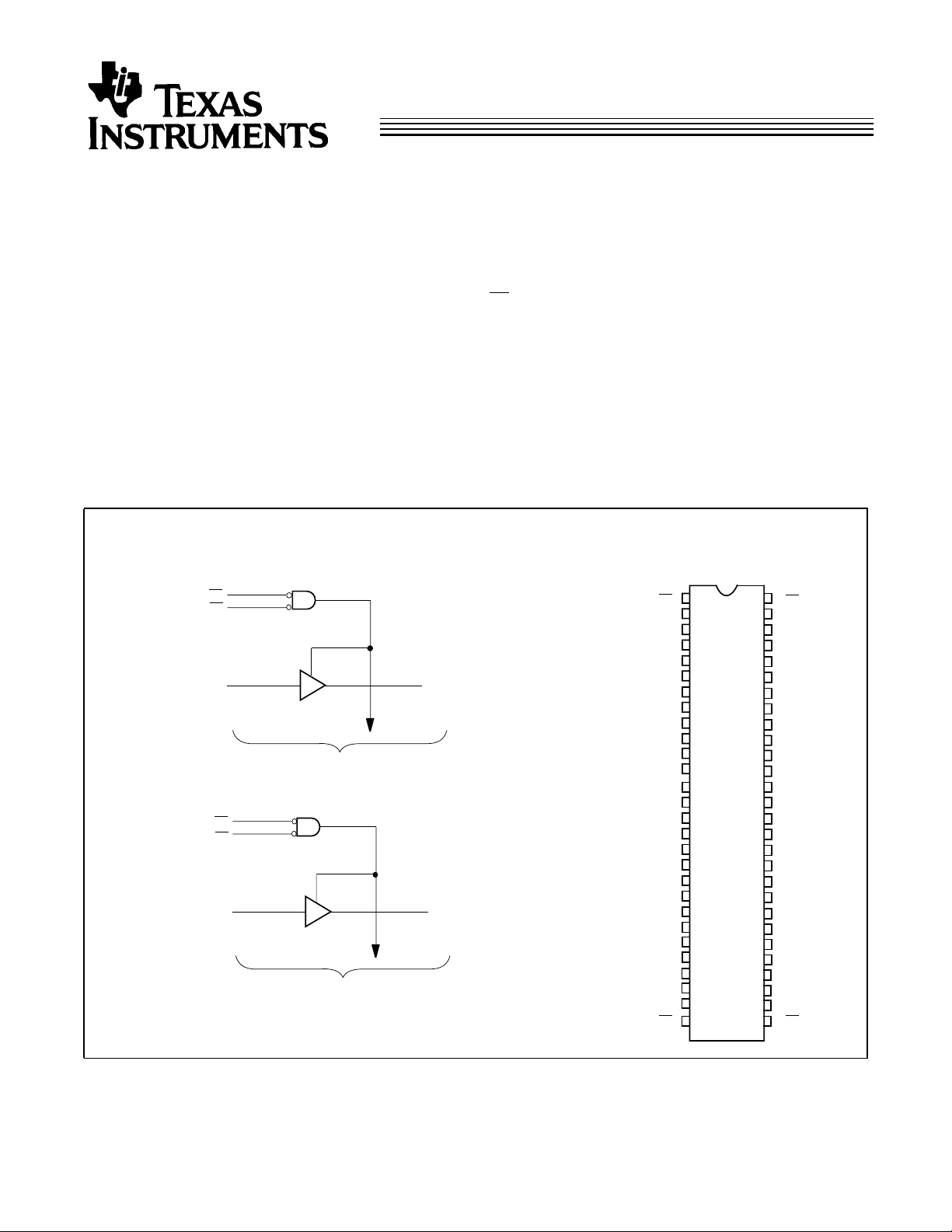
The CY74FCT163827 is a 20-bit buffer/linedriver that provides
high-performance bus interf ace b uff ering for wide data/address
paths or buses carrying parity . It can be used as a single 20-bit
bufferortwo 10-bit buffers.Each 10-bitbufferhasa pair of NANDed
OE for increased flexibility.
The CY74FCT163827 has 24-mA balanced output drivers
with current limiting resistors in the outputs. This reduces the
need for external terminating resistors and provides for
minimal undershoot and reduced ground bounce. The inputs
and outputs were designed to be capable of being driven by
5.0V buses, allowing its use in mixed voltage systems as a
translator. The outputs are also designed with a power-off
disable feature enabling its use in applications requiring live
insertion.
20-Bit Buffe
• ESD (HBM) > 2000V
Logic Block Diagrams CY74FCT163827 Pin Configuration
SSOP/TSSOP
Top View
1OE1
1OE2
1A1
2OE1
2OE2
2A1
TO 9 OTHER CHANNELS
TO 9 OTHER CHANNELS
1Y1
FCT163827-1
2Y1
FCT163827-2
1OE1
1Y1
1Y2
GND
1Y3
1Y4
V
1Y5
1Y6
1Y7
GND
1Y8
1Y9
1Y10
2Y1
2Y2
2Y3
GND
2Y4
2Y5
2Y6
V
2Y7
2Y8
GND
2Y9
2Y10
2OE1
1
2
3
4
5
6
CC
7
8
9
10
11
12
13
14
15
16
17
18
19
20
21
CC
22
23
24
25
26
27
28
56
55
54
53
52
51
50
49
48
47
46
45
44
43
42
41
40
39
38
37
36
35
34
33
32
31
30
29
1OE2
1A1
1A2
GND
1A3
1A4
V
CC
1A5
1A6
1A7
GND
1A8
1A9
1A10
2A1
2A2
2A3
GND
2A4
2A5
2A6
V
CC
2A7
2A8
GND
2A9
2A10
2OE2
Copyright © 2000, Texas Instruments Incorporated
CY74FCT163827
Pin Description
Name Description
OE Output Enable Inputs (Active LOW)
A Data Inputs
Y Three-State Outputs
Function Table
OE
1
L L L L
L L H H
H X X Z
X H X Z
[1]
Inputs Outputs
OE
2
A Y
Maximum Ratings
(Above which the useful life may be impaired. For user
guidelines, not tested.)
Storage Temperature ................................ −55°C to +125°C
Ambient Temperature with
Power Applied............................................ −55°C to +125°C
Supply Voltage Range..................................... 0.5V to +4.6V
DC Input Voltage .................................................−0.5V to +7.0V
DC Output Voltage..............................................−0.5V to +7.0V
DC Output Current
(Maximum Sink Current/Pin)...........................−60 to +120 mA
Power Dissipation..........................................................1.0W
Operating Range
Range
[2, 3]
Ambient
Temperature V
CC
Commercial –40°C to +85°C 2.7V to 3.6V
Electrical Characteristics Over the Operating Range V
Parameter Description Test Conditions Min. Typ.
V
IH
V
IL
V
H
V
IK
I
IH
I
IL
I
OZH
I
OZL
I
OS
I
OFF
I
CC
∆I
CC
Note:
1. H = HIGH Voltage Level, L = LOW Voltage Level, X = Don’t Care, Z = HIGH Impedance.
2. Operation beyond the limits set forth may impair the useful life of the device. Unless otherwise noted, these limits are over the operating free-air temperature
range.
3. Unused inputs must always be connected to an appropriate logic voltage level, preferably either V
4. Typical values are at V
5. This parameter is specified but not tested.
6. Not more than one output should be shorted at a time. Duration of short should not exceed one second. The use of high-speed test apparatus and/or sample
and hold techniques are preferable in order to minimize internalchip heating and more accurately reflect operational values. Otherwise prolonged shorting of
a high output may raise the chip temperature well above normal and thereby cause invalid readings in other parametric tests. In any sequence of parameter
tests, I
7. Per TTL driven input; all other inputs at V
Input HIGH Voltage All Inputs 2.0 5.5 V
Input LOW Voltage 0.8 V
Input Hysteresis
[5]
Input Clamp Diode Voltage VCC=Min., IIN=–18 mA –0.7 – 1.2 V
Input HIGH Current VCC=Max., VI=5.5 ±1 µA
Input LOW Current VCC=Max., VI=GND ±1 µA
High Impedance Output Current
VCC=Max., V
(Three-State Output pins)
High Impedance Output Current
VCC=Max., V
(Three-State Output pins)
Short Circuit Current
[6]
VCC=Max., V
Power-Off Disable VCC=0V, V
Quiescent Power Supply Current VIN≤0.2V,
V
Quiescent Power Supply Current
VIN=VCC–0.6V
(TTL inputs HIGH)
=3.3V, TA = +25˚C ambient.
CC
tests should be performed last.
OS
or GND.
CC
CC
IN>VCC
=2.7V to 3.6V
[4]
100 mV
=5.5V ±1 µA
OUT
=GND ±1 µA
OUT
=GND –60 –135 –240 mA
OUT
≤4.5V ±100 µA
OUT
VCC=Max. 0.1 10 µA
–0.2V
[7]
VCC=Max. 2.0 30 µA
or ground.
CC
Max. Unit
2
 Loading...