


Texas Instruments CD74HCT4053PWR, CD74HCT4053M96, CD74HCT4053M, CD74HCT4053E, CD74HCT4052M96 Datasheet
...[ /Title (CD54 HC405 1, CD74 HC405 1, CD74 HCT40 51, CD74 HC405 2,
Data sheet acquired from Harris Semiconductor SCHS122A
November 1997 - Revised April 1999
CD54HC4051, CD74HC4051, CD74HCT4051, CD74HC4052, CD74HCT4052, CD74HC4053, CD74HCT4053
High Speed CMOS Logic Analog Multiplexers/Demultiplexers
Features
• Wide Analog Input Voltage Range . . . . . . . . . .±5V Max
•Low “On” Resistance
-70Ω Typical (VCC - VEE = 4.5V)
-40Ω Typical (VCC - VEE = 9V)
•Low Crosstalk between Switches
•Fast Switching and Propagation Speeds
•“Break-Before-Make” Switching
• Wide Operating Temperature Range . . -55oC to 125oC
• CD54HC/CD74HC Types |
|
|
|
- |
Operation Control Voltage . . . . |
. . . . . . . . . . 2V to 6V |
|
- |
Switch Voltage . . . . . . . |
. . . . . . . . |
. . . . . . . . 0V to 10V |
- |
High Noise Immunity . . . |
NIL = 30%, NIH = 30% of VCC, |
|
|
VCC = 5V |
|
|
• CD54HCT/CD74HCT Types |
|
||
- |
Operation Control Voltage . . . . . |
. . . . . . 4.5V to 5.5V |
|
- |
Switch Voltage . . . . . . . |
. . . . . . . . |
. . . . . . . . 0V to 10V |
- |
Direct LSTTL Input |
|
|
|
Logic Compatibility . . . |
VIL = 0.8V Max, VIH = 2V Min |
|
- |
CMOS Input Compatibility . . . . . |
II ≤ 1μA at VOL, VOH |
|
Description
These devices are digitally controlled analog switches which utilize silicon gate CMOS technology to achieve operating speeds similar to LSTTL with the low power consumption of standard CMOS integrated circuits.
These analog multiplexers/demultiplexers control analog voltages that may vary across the voltage supply range (i.e. VCC to VEE). They are bidirectional switches thus allowing any analog input to be used as an output and visa-versa. The switches have low “on” resistance and low “off” leakages. In addition, all three devices have an enable control which, when high, disables all switches to their “off” state.
Ordering Information
|
TEMP. |
|
PKG. |
PART NUMBER |
RANGE (oC) |
PACKAGE |
NO. |
CD54HC4051F |
-55 to 125 |
16 Ld CERDIP |
F16.3 |
|
|
|
|
CD74HC4051E |
-55 to 125 |
16 Ld PDIP |
E16.3 |
|
|
|
|
CD74HC4052E |
-55 to 125 |
16 Ld PDIP |
E16.3 |
|
|
|
|
CD74HC4053E |
-55 to 125 |
16 Ld PDIP |
E16.3 |
|
|
|
|
CD74HCT4051E |
-55 to 125 |
16 Ld PDIP |
E16.3 |
|
|
|
|
CD74HCT4052E |
-55 to 125 |
16 Ld PDIP |
E16.3 |
|
|
|
|
CD74HCT4053E |
-55 to 125 |
16 Ld PDIP |
E16.3 |
|
|
|
|
CD74HC4051M |
-55 to 125 |
16 Ld SOIC |
M16.15 |
|
|
|
|
CD74HC4052M |
-55 to 125 |
16 Ld SOIC |
M16.15 |
|
|
|
|
CD74HC4053M |
-55 to 125 |
16 Ld SOIC |
M16.15 |
|
|
|
|
CD74HCT4051M |
-55 to 125 |
16 Ld SOIC |
M16.15 |
|
|
|
|
CD74HCT4052M |
-55 to 125 |
16 Ld SOIC |
M16.15 |
|
|
|
|
CD74HCT4053M |
-55 to 125 |
16 Ld SOIC |
M16.15 |
|
|
|
|
CD74HCT4053PW |
-55 to 125 |
16 Ld TSSOP |
|
|
|
|
|
CD74HCT4052SM |
-55 to 125 |
16 Ld SSOP |
M16.15A |
|
|
|
|
NOTES: |
|
|
|
1.When ordering, use the entire part number. Add the suffix 96 to obtain the variant in the tape and reel. For the TSSOP package only, add the suffix R to obtain the variant in the tape and reel.
2.Wafer or die is available which meets all electrical specifications. Please contact your local sales office or Harris customer service for ordering information.
CAUTION: These devices are sensitive to electrostatic discharge. Users should follow proper IC Handling Procedures. |
File Number 1676.1 |
|
|
||
Copyright © Harris Corporation 1997 |
1 |
|
|
|
|

CD54HC4051, CD74HC4051, 52, 53; CD74HCT4051, 52, 53
Pinouts
CD54HC4051
CD74HC4051, CD74HCT4051
(CERDIP, PDIP, SOIC)
TOP VIEW
CHANNEL |
A4 |
1 |
IN/OUT |
A6 |
2 |
|
COM OUT/IN |
A |
3 |
CHANNEL |
A7 |
4 |
IN/OUT |
A5 |
5 |
|
E |
6 |
VEE |
7 |
GND |
8 |
16 VCC |
15 |
A2 |
14 |
A1 |
CHANNEL |
|
|
|
13 |
A0 |
IN/OUT |
|
12 |
A3 |
11 |
S0 |
10 S1 |
ADDRESS |
|
SELECT |
9 |
S2 |
CD74HC4052, CD74HCT4052
(PDIP, SOIC)
TOP VIEW
CHANNEL |
B0 |
1 |
|
|
|
IN/OUT |
B2 |
2 |
|
COM OUT/IN BN |
3 |
CHANNEL |
B3 |
4 |
|
|
|
IN/OUT |
B1 |
5 |
|
E |
6 |
VEE |
7 |
GND |
8 |
16 VCC |
15 |
A2 |
CHANNEL |
|
|
|
14 |
A1 |
IN/OUT |
|
||
13 |
AN |
COM OUT/IN |
12 |
A0 |
CHANNEL |
|
|
|
11 |
A3 |
IN/OUT |
10 |
S0 |
9 |
S1 |
CD74HC4053, CD74HCT4053
(PDIP, SOIC, TSSOP)
TOP VIEW
B1 |
1 |
CHANNEL |
B0 |
2 |
|
IN/OUT |
|||
|
|
C1 |
3 |
COM OUT/IN CN |
4 |
IN/OUT C0 |
5 |
E |
6 |
VEE |
7 |
GND |
8 |
16 VCC |
15 |
BN |
COM OUT/IN |
14 |
AN |
COM OUT/IN |
13 |
A1 |
CHANNEL |
|
|
|
12 |
A0 |
IN/OUT |
11 |
S0 |
|
10 |
S1 |
9 |
S2 |
2

CD54HC4051, CD74HC4051, 52, 53; CD74HCT4051, 52, 53
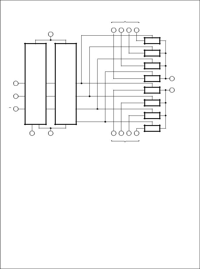
Functional Diagram of HC/HCT4051
|
|
|
CHANNEL IN/OUT |
|
|
|||
VCC |
A7 |
A6 |
A5 |
A4 |
A3 |
A2 |
A1 |
A0 |
16 |
4 |
2 |
5 |
1 |
12 |
15 |
14 |
13 |
TG |
TG
S0 11
|
|
|
TG |
S1 |
10 |
|
TG |
BINARY |
A |
||
|
|
3 COMMON |
|
|
LOGIC |
TO |
OUT/IN |
|
1 OF 8 |
||
|
LEVEL |
TG |
|
|
DECODER |
||
|
CONVERSION |
|
|
|
WITH |
|
|
|
|
|
|
S2 |
9 |
ENABLE |
|
|
TG |
||
|
|
|
|
|
|
|
TG |
E |
6 |
|
|
|
|
|
TG |
8 |
7 |
GND VEE
TRUTH TABLE
CD54/74HC/HCT4051
|
INPUT STATES |
|
“ON” |
|
|
|
|
|
|
ENABLE |
S2 |
S1 |
S0 |
CHANNELS |
L |
L |
L |
L |
A0 |
|
|
|
|
|
L |
L |
L |
H |
A1 |
|
|
|
|
|
L |
L |
H |
L |
A2 |
|
|
|
|
|
L |
L |
H |
H |
A3 |
|
|
|
|
|
L |
H |
L |
L |
A4 |
|
|
|
|
|
L |
H |
L |
H |
A5 |
|
|
|
|
|
L |
H |
H |
L |
A6 |
|
|
|
|
|
L |
H |
H |
H |
A7 |
|
|
|
|
|
H |
X |
X |
X |
None |
|
|
|
|
|
X = Don’t care
3
CD54HC4051, CD74HC4051, 52, 53; CD74HCT4051, 52, 53
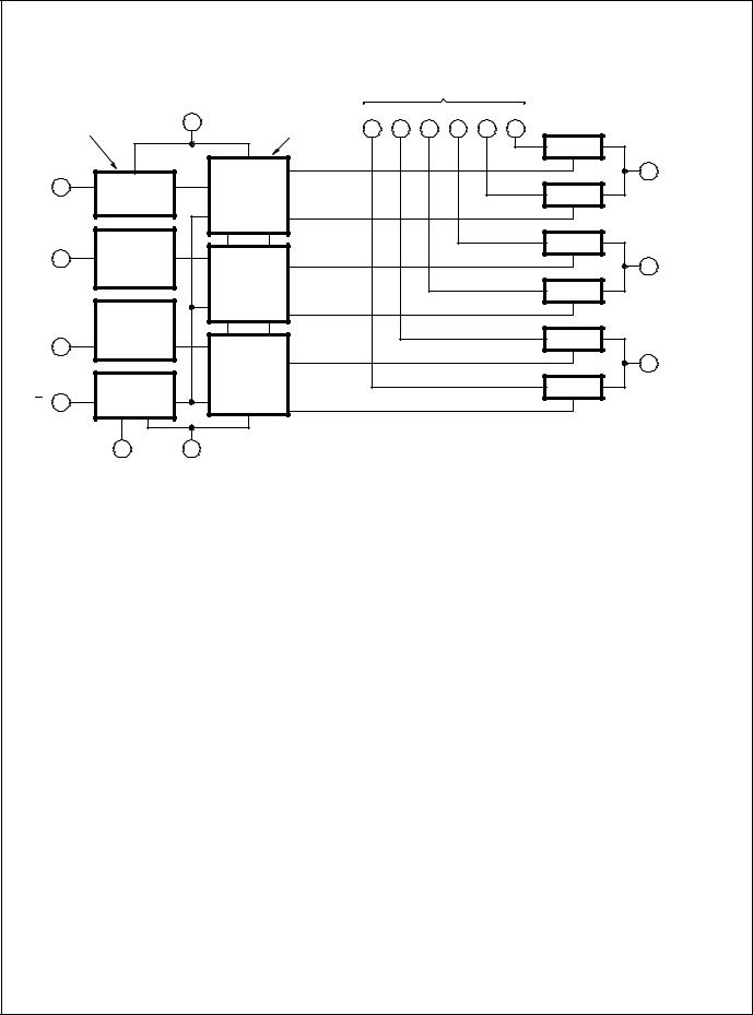
Functional Diagram of HC/HCT4052
|
A CHANNELS IN/OUT |
||||
VCC |
A3 |
A2 |
A1 |
A0 |
|
11 |
15 |
14 |
12 |
||
|
|||||
16 |
|
|
|
|
|
|
|
|
BINARY |
|
S1 |
9 |
LOGIC |
TO |
|
1 OF 4 |
||||
LEVEL |
||||
|
|
CONVERSION |
DECODER |
|
|
|
WITH |
||
|
|
|
||
|
|
|
ENABLE |
|
S0 |
10 |
|
|
|
E |
6 |
|
|
8 |
7 |
GND VEE
TRUTH TABLE
CD74HC4052, CD74HCT4052
|
INPUT STATES |
|
“ON” |
||
|
|
|
|
|
|
ENABLE |
|
S1 |
|
S0 |
CHANNELS |
L |
|
L |
|
L |
A0, B0 |
|
|
|
|
|
|
L |
|
L |
|
H |
A1, B1 |
|
|
|
|
|
|
L |
|
H |
|
L |
A2. B2 |
|
|
|
|
|
|
L |
|
H |
|
H |
A3, B3 |
|
|
|
|
|
|
H |
|
X |
|
X |
None |
|
|
|
|
|
|
X = Don’t care
1 |
5 |
2 |
4 |
B0 |
B1 |
B2 |
B3 |
B CHANNELS IN/OUT
TG
TG
TG |
|
|
|
TG |
13 |
COMMON A |
|
OUT/IN |
|||
|
|
||
TG |
3 |
COMMON B |
|
OUT/IN |
|||
|
|
||
TG |
|
|
TG
TG
4
CD54HC4051, CD74HC4051, 52, 53; CD74HCT4051, 52, 53
Functional Diagram of HC/HCT4053
|
|
VCC |
BINARY TO |
|
|
IN/OUT |
|
|
|
|
|
|
|
|
|
|
|
|
|
||
|
|
1 OF 2 |
C1 |
C0 |
B1 |
B0 |
A1 |
A0 |
|
|
|
LOGIC LEVEL |
16 |
DECODERS |
|
||||||
|
|
|
|
|
|
|
|
|||
|
CONVERSION |
WITH ENABLE |
3 |
5 |
1 |
2 |
13 |
12 |
|
|
|
|
|
||||||||
|
|
|
|
|
|
|
|
|
TG |
|
|
|
|
|
|
|
|
|
|
14 |
A COMMON |
|
|
|
|
|
|
|
|
|
OUT/IN |
|
S0 |
11 |
|
|
|
|
|
|
|
|
|
|
|
|
|
|
|
|
TG |
|
||
|
|
|
|
|
|
|
|
|
|
|
|
|
|
|
|
|
|
|
|
TG |
|
S1 |
10 |
|
|
|
|
|
|
|
15 |
B COMMON |
|
|
|
|
|
|
|
|
|
OUT/IN |
|
|
|
|
|
|
|
|
|
|
|
|
|
|
|
|
|
|
|
|
|
TG |
|
S2 |
9 |
|
|
|
|
|
|
|
TG |
|
|
|
|
|
|
|
|
|
C COMMON |
||
|
|
|
|
|
|
|
|
|
4 |
|
|
|
|
|
|
|
|
|
|
OUT/IN |
|
|
|
|
|
|
|
|
|
|
|
|
|
|
|
|
|
|
|
|
|
TG |
|
E |
6 |
|
|
|
|
|
|
|
|
|
|
8 |
7 |
|
|
|
|
|
|
|
|
|
GND |
VEE |
|
|
|
|
|
|
|
|
TRUTH TABLE
CD74HC4053, CD74HCT4053
|
INPUT STATES |
|
“ON” |
|
|
|
|
|
|
ENABLE |
S0 |
S1 |
S2 |
CHANNELS |
L |
L |
L |
L |
C0, B0, A0 |
|
|
|
|
|
L |
H |
L |
L |
C0, B0, A1 |
|
|
|
|
|
L |
L |
H |
L |
C0, B1, A0 |
|
|
|
|
|
L |
H |
H |
L |
C0, B1, A1 |
|
|
|
|
|
L |
L |
L |
H |
C1, B0, A0 |
|
|
|
|
|
L |
H |
L |
H |
C1, B0, A1 |
|
|
|
|
|
L |
L |
H |
H |
C1, B1, A0 |
|
|
|
|
|
L |
H |
H |
H |
C1, B1, A1 |
|
|
|
|
|
H |
X |
X |
X |
None |
|
|
|
|
|
X = Don’t care
5
CD54HC4051, CD74HC4051, 52, 53; CD74HCT4051, 52, 53
Absolute Maximum Ratings (Note 3) |
|
Thermal Information |
|
|
|
|
|
||
DC Supply Voltage, V |
CC |
- V . . . . . . . . . . . . . . . . . |
-0.5V to 10.5V |
Thermal Resistance (Typical, Note 4) |
θ |
JA |
(oC/W) θ |
JC |
(oC/W) |
|
EE |
|
|
|
|
|
|||
DC Supply Voltage, VCC |
. . . . . . . . . . . . . . . . . . . . . . . . . |
. . . -0.5V to +7V |
PDIP Package . . . . . . . . . . . . . . . . . . . |
|
|
90 |
|
N/A |
|
DC Supply Voltage, VEE . |
. . . . . . . . . . . . . . . . . . . . . . . . . |
. . +0.5V to -7V |
SOIC Package . . . . . . . . . . . . . . . . . . . |
|
|
160 |
|
N/A |
|
DC Input Diode Current, IIK |
±20mA |
CERDIP Package . . . . . . . . . . . . . . . . |
|
|
130 |
|
55 |
||
For VI < -0.5V or VI > VCC + 0.5V . . . . . . . . . . . . . . . . |
TSSOP Package . . . . . . . . . . . . . . . . . |
|
|
149 |
|
35 |
|||
DC Switch Diode Current, IOK |
|
Maximum Junction Temperature . . . . . . . . |
. . |
. |
. . . . . . . . . |
. . |
. 150oC |
||
For VI < VEE -0.5V or VI > VCC + 0.5V . . . . . . . . . . . |
. . . . . .±20mA |
Maximum Storage Temperature Range . . . |
. |
. . |
. . . .-65oC to 150oC |
||||
DC Switch Current, (Note 2) |
|
Maximum Lead Temperature (Soldering 10s) . . |
. . . . . . . . |
. . |
. 300oC |
||||
For VI > VEE -0.5V or VI < VCC + 0.5V . . . . . . . . . . . |
. . . . . .±25mA |
|
|
|
|
|
|
||
DC VCC or Ground Current, ICC . . . . . . . . . . . . . . . . . . . |
. . . . . .±50mA |
|
|
|
|
|
|
||
DC VEE Current, IEE |
. . . |
. . . . . . . . . . . . . . . . . . . . . . . |
. . . . . -20mA |
|
|
|
|
|
|
Recommended Operating Conditions For maximum reliability, nominal operating conditions should be selected so that operation is always within the following ranges
|
PARAMETER |
MIN |
MAX |
UNITS |
|
|
|
|
|
Supply Voltage Range (For TA = Full Package Temperature Range), VCC (Note 5) |
|
|
|
|
|
CD54/74HC Types |
2 |
6 |
V |
|
|
|
|
|
|
CD54/74HCT Types |
4.5 |
5.5 |
V |
|
|
|
|
|
Supply Voltage Range (For TA = Full Package Temperature Range), VCC - VEE |
|
|
|
|
|
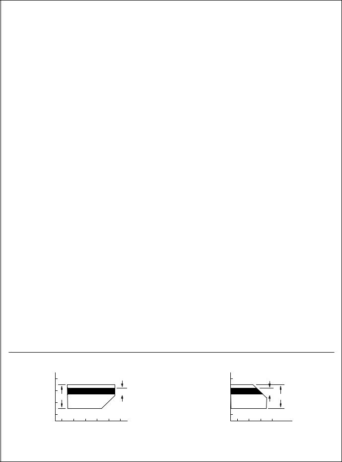
CD54/74HC Types, CD54/74HCT Types (See Figure 1) |
2 |
10 |
V |
|
|
|
|
|
Supply Voltage Range (For TA = Full Package Temperature Range), VEE (Note 5) |
|
|
|
|
|
CD54/74HC Types, CD54/74HCT Types (See Figure 2) |
0 |
-6 |
V |
|
|
|
|
|
DC Input Control Voltage, VI |
GND |
VCC |
V |
|
Analog Switch I/O Voltage, VIS |
VEE |
VCC |
V |
|
Operating Temperature, T |
-55 |
125 |
oC |
|
|
A |
|
|
|
Input Rise and Fall Times, tr, tf |
|
|
|
|
|
2V |
0 |
1000 |
ns |
|
|
|
|
|
|
4.5V |
0 |
500 |
ns |
|
|
|
|
|
|
6V |
0 |
400 |
ns |
|
|
|
|
|
CAUTION: Stresses above those listed in “Absolute Maximum Ratings” may cause permanent damage to the device. This is a stress only rating and operation of the device at these or any other conditions above those indicated in the operational sections of this specification is not implied.
NOTES:
3.All voltages referenced to GND unless otherwise specified.
4.θJA is measured with the component mounted on an evaluation PC board in free air.
5.In certain applications, the external load resistor current may include both VCC and signal line components. To avoid drawing VCC current when switch current flows into the transmission gate inputs, the voltage drop across the bidirectional switch must not exceed 0.6V (cal-
culated from rON values shown in Electrical Specifications table). No VCC current will flow through RL if the switch current flows into terminal 3 on the HC/HCT4051; terminals 3 and 13 on the HC/HCT4052; terminals 4, 14 and 15 on the HC/HCT4053.
Recommended Operating Area as a Function of Supply Voltages
|
8 |
|
|
|
|
|
|
(V) |
6 |
|
|
|
|
|
|
GND |
|
HC |
|
|
|
|
HCT |
4 |
|
|
|
|
|
||
- |
|
|
|
|
|
|
|
CC |
2 |
|
|
|
|
|
|
V |
|
|
|
|
|
|
|
|
|
|
|
|
|
|
|
|
0 |
2 |
4 |
6 |
8 |
10 |
12 |
|
0 |
||||||
|
|
|
VCC - VEE (V) |
|
|
||
|
8 |
|
|
|
|
(V) |
6 |
|
|
|
|
GND |
|
|
|
HCT |
HC |
4 |
|
|
|
||
- |
|
|
|
|
|
CC |
2 |
|
|
|
|
V |
|
|
|
|
|
|
|
|
|
|
|
|
0 |
-2 |
-4 |
-6 |
-8 |
|
0 |
||||
|
|
|
VEE - GND (V) |
||
FIGURE 1. |
FIGURE 2. |
6
 Loading...