


CY74FCT2573TSOCT
Texas Instruments CY74FCT2573TSOCT, CY74FCT2573TSOC, CY74FCT2573CTSOCT, CY74FCT2573CTSOC, CY74FCT2573CTQCT Datasheet
...
8-Bit Latches
CY74FCT2373T
CY74FCT2573T
SCCS039 - September 1994 - Revised March 2000
Data sheet acquired from Cypress Semiconductor Corporation.
Data sheet modified to remove devices not offered.
Copyright © 2000, Texas Instruments Incorporated
1CY74FCT2573T
Features
• Functionandpinoutcompatiblewiththefastestbipolar
logic
•25Ωoutputseries resistors to reduce transmissionline
refelection noise
• FCT-C speed at 4.7 ns max.
• Reduced V
OH
(typically=3.3V) versions of equivalent
FCT functions
• Edge-rate control circuitry for significantly improved
noise characteristics
• Power-off disable feature
• Matched rise and fall times
• ESD > 2000V
• Fully compatible with TTL input and output logic levels
• Sink current 12 mA
Source current 15 mA
• Extended commercial temp. range of –40˚C to +85˚C
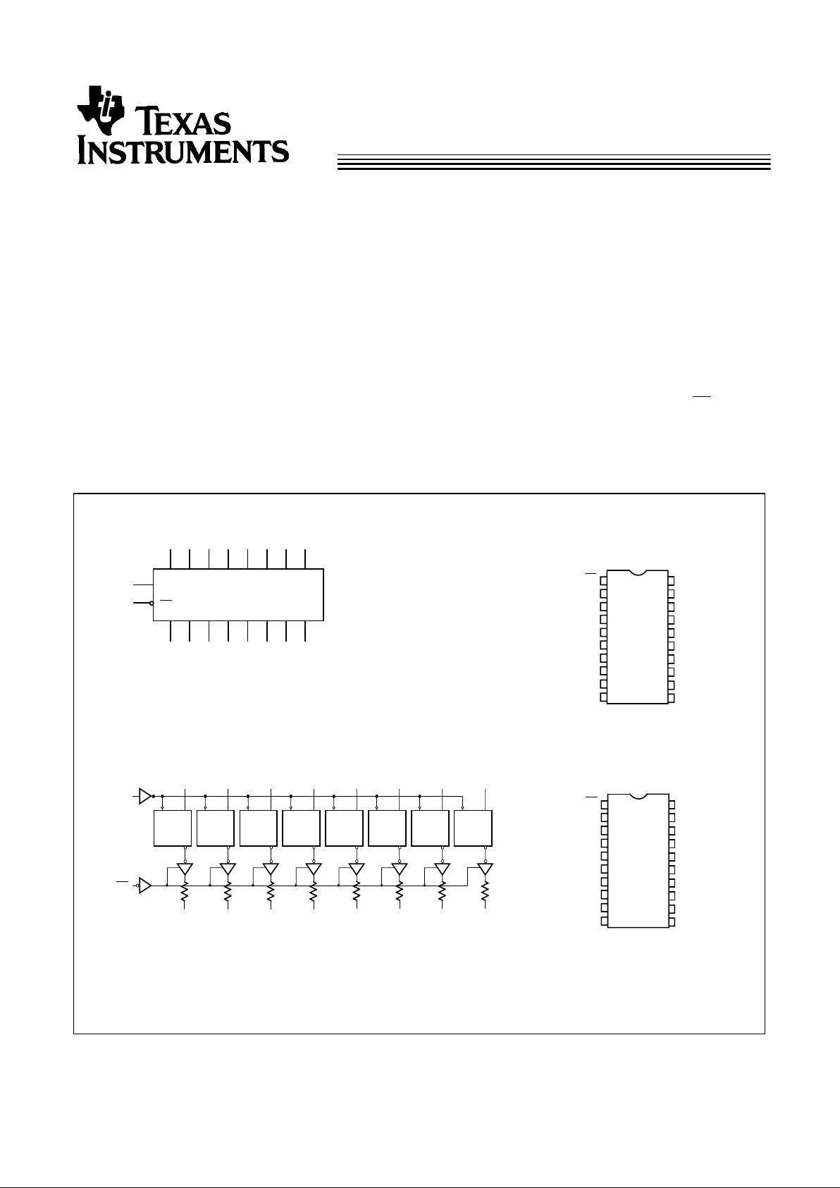
Functional Description
The FCT2373T and FCT2573T are 8-bit, high-speed CMOS
TTL-compatible buffered latches with three-state outputs that
are ideal for driving high-capacitance loads, such as memory
and address buffers. On-chip 25Ω termination resistors have
been added to the outputs to reduce system noise caused by
reflections. FCT2373T can be used to replace FCT373T, and
FCT2573T to replace FCT573T to reduce noise in an existing
design.
When latch enable (LE) is HIGH, the flip-flops appear transparent to the data. Data that meets the required set-up times
are latched when LE transitions from HIGH to LOW. Data
appears on the bus when the output enable (
OE) is LOW.
When output enable is HIGH, the bus output is in the high
impedance state. In this mode, data can still be entered into
the latches.
The outputs are designed with a power-off disable feature to
allow for live insertion of boards.
FCT2373T-1
Logic Block Diagram
PinConfigurations
1
2
3
4
5
6
7
8
9
10
11
12
16
17
18
19
20
13
14
V
CC
15
SOIC/QSOP
Top View
O
0
D
0
D
1
O
2
D
2
D
3
O
3
D
7
D
6
O
6
O
5
D
5
D
4
O
4
LE
OE
GND
O
7
O
1
CP D
Q
O
0
D
0
LE
OE
CP D
Q
O
1
D
1
CP D
Q
O
2
D
2
CP D
Q
O
3
D
3
CP D
Q
O
4
D
4
CP D
Q
O
5
D
5
CP D
Q
O
6
D
6
CP D
Q
O
7
D
7
FCT2373T-2
Logic Symbol
FCT2373T
LE
OE
D
0
O
0
D
1
O
1
D
2
O
2
D
3
O
3
D
4
O
4
D
5
O
5
D
6
O
6
D
7
O
7
FCT2373T-4
1
2
3
4
5
6
7
8
9
10
11
12
16
17
18
19
20
13
14
V
CC
15
SOIC/QSOP
Top View
D
0
D
1
D
2
D
4
D
5
D
6
D
7
O
1
O
2
O
3
O
4
O
5
O
6
O
7
LE
OE
GND
O
0
D
3
FCT2373T-6
CY74FCT2373T
CY74FCT2573T
2
Maximum Ratings
[2, 3]
(Above which the useful life may be impaired. For user guidelines, not tested.)
Storage Temperature .................................–65°C to +150°C
Ambient Temperature with
Power Applied.............................................–65°C to +135°C
Supply Voltage to Ground Potential............... –0.5V to +7.0V
DC Input Voltage ........................................... –0.5V to +7.0V
DC Output Voltage......................................... –0.5V to +7.0V
DC Output Current (Maximum Sink Current/Pin) ......120 mA
Power Dissipation..........................................................0.5W
Static Discharge Voltage............................................>2001V
(per MIL-STD-883, Method 3015)
Function Table
[1]
Inputs Outputs
OE LE D O
L H H H
L H L L
L L X Q
0
H X X Z
Operating Range
Range
Ambient
Temperature V
CC
Commercial –40°C to +85°C 5V ± 5%
Electrical Characteristics Over the Operating Range
Parameter Description Test Conditions Min. Typ.
[5]
Max. Unit
V
OH
Output HIGH Voltage VCC=Min., IOH=–15 mA 2.4 3.3 V
V
OL
Output LOW Voltage VCC=Min., IOL=12 mA 0.3 0.55 V
R
OUT
Output Resistance VCC=Min., IOL=12 mA 20 28 40 Ω
V
IH
Input HIGH Voltage 2.0 V
V
IL
Input LOW Voltage 0.8 V
V
H
Hysteresis
[6]
All inputs 0.2 V
V
IK
Input Clamp Diode Voltage VCC=Min., IIN=–18 mA –0.7 –1.2 V
I
I
Input HIGH Current VCC=Max., VIN=V
CC
5 µA
I
IH
Input HIGH Current VCC=Max., VIN=2.7V ±1 µA
I
IL
Input LOW Current VCC=Max., VIN=0.5V ±1 µA
I
OZH
Off State HIGH-Level Output
Current
VCC=Max., V
OUT
=2.7V 10 µA
I
OZL
Off State LOW-Level
Output Current
VCC=Max., V
OUT
=0.5V –10 µA
I
OS
Output Short Circuit Current
[7]
VCC=Max., V
OUT
=0.0V –60 –120 –225 mA
I
OFF
Power-Off Disable VCC=0V, V
OUT
=4.5V ±1 µA
Notes:
1. H = HIGH Voltage Level
L = LOW Voltage Level
X = Don’t Care
Z = HIGH Impedance
Q
n
= Previous state of flip flops (Q
n–1
)
2. Unless otherwise noted, these limits are over the operating free-air temperature range.
3. Unused inputs must always be connected to an appropriate logic voltage level, preferably either V
CC
or ground.
4. T
A
is the “instant on” case temperature.
5. Typical values are at V
CC
=5.0V, TA=+25˚C ambient.
6. This parameter is specified but not tested.
7. Not more than one output should be shorted at a time. Duration of short should not exceed one second. The use of high-speed test apparatus and/or sample
and hold techniques are preferable in order to minimize internal chip heating and more accurately reflect operational values. Otherwise prolonged shorting
of a high output may raise the chip temperature well above normal and thereby cause invalid readings in other parametric tests. In any sequence of parameter
tests, I
OS
tests should be performed last.
 Loading...