


CY74FCT245TSOCT
Texas Instruments CY74FCT245TSOCT, CY74FCT245TSOC, CY74FCT245CTQCT, CY74FCT245CTQC, CY74FCT245ATSOCT Datasheet
...
8-Bit Transceive
r
CY54/74FCT245T
SCCS018 - May 1994 - Revised February 2000
Data sheet acquired from Cypress Semiconductor Corporation.
Data sheet modified to remove devices not offered.
Copyright © 2000, Texas Instruments Incorporated
Features
• Function, pinout, and drive compatible with FCT, and
F logic
• FCT-D speed at 3.8 ns max. (Com’l),
FCT-C speed at 4.1 ns max. (Com’l),
FCT-A speed at 4.6 ns max. (Com’l)
• Reduced V
OH
(typically = 3.3V) versions of equivalent
FCT functions
• Edge-rate control circuitry for significantly improved
noise characteristics
• Power-off disable feature
• ESD > 2000V
• Matched rise and fall times
• Fully compatible with TTL input and output logic levels
• Extended commercial range of −40˚C to +85˚C
• Sink current 64 mA (Com’l), 48 mA (Mil)
Source current 32 mA (Com’l), 12 mA (Mil)
Functional Description
The FCT245T contains eight non-inverting bidirectional buff-
ers with three-state outputs and is intended for bus oriented
applications. For the FCT245T,current sinking capability is 64
mA at the A and B ports.
The Transmit/Receiver (T/
R) input determines the direction of
data flow through bidirectional transceiver. Transmit (Active
HIGH)enablesdatafromAports to Bports. The output enable
(
OE), when HIGH, disables both the A and B ports by putting
them in a High Z condition.
The outputs are designed with a power-off disable feature to
allow for live insertion of boards.
Function Table
[1]
OE T/R Operation
L L B Data to Bus A
L H A Data to Bus B
H X High Z State
Note:
1. H = HIGH Voltage Level. L = LOW Voltage Level. X = Don’t Care.
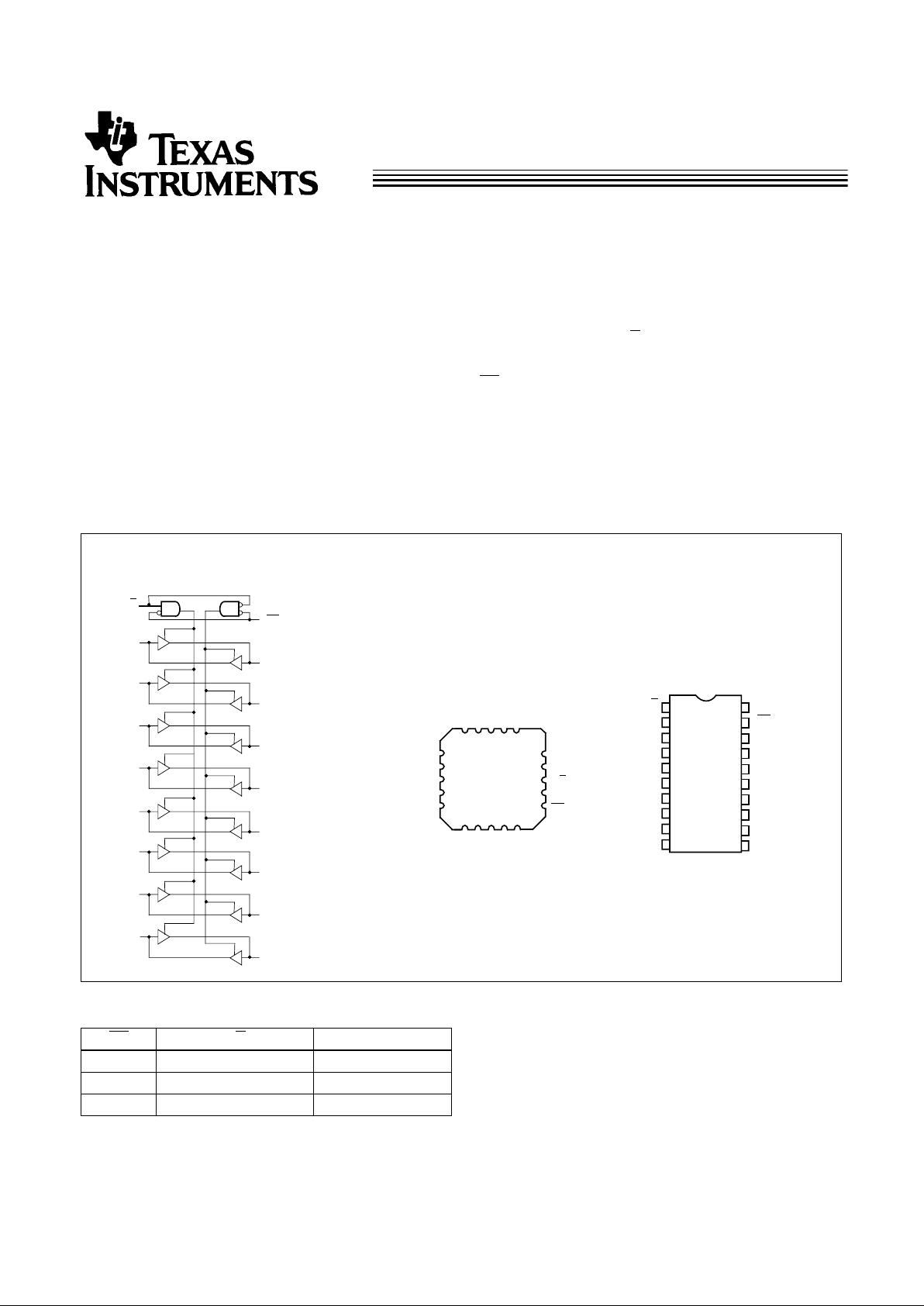
LogicBlockDiagram Pin Configurations
A
0
A
1
A
2
A
3
A
4
A
5
A
6
A
7
OE
B
0
B
1
B
2
B
3
B
4
B
5
B
6
B
7
T/R
4
8
9
10
11
12
765
1516 17 18
3
2
1
20
13
14
19
A
6
A
5
A
3
B
1
B
4
B
0
B
7
V
CC
GND
B
3
Top View
A
2
LCC
T/R
A
0
A
1
A
7
B
5
B
6
1
2
3
4
5
6
7
8
9
10
11
12
16
17
18
19
20
13
14
V
CC
15
Top View
B
2
A
4
OE
A
0
A
1
A
2
A
3
A
4
A
5
A
6
A
7
OE
B
0
B
1
B
2
B
3
B
4
B
5
B
6
B
7
T/R
GND
DIP/SOIC/QSOP
CY54/74FCT245T
2
Maximum Ratings
[2,3]
(Above which the useful life may be impaired. For user
guidelines, not tested.)
Storage Temperature .....................................−65°C to +150°C
Ambient Temperature with
Power Applied..................................................−65°C to +135°C
Supply Voltage to Ground Potential..................−0.5V to +7.0V
DC Input Voltage .................................................−0.5V to +7.0V
DC Output Voltage..............................................−0.5V to +7.0V
DC Output Current (Maximum Sink Current/Pin).......120 mA
Power Dissipation..........................................................0.5W
Static Discharge Voltage............................................>2001V
(per MIL-STD-883, Method 3015)
Operating Range
Range Range
Ambient
Temperature V
CC
Commercial DT 0°C to +70°C 5V ± 5%
Commercial T, AT, CT −40°C to +85°C 5V ± 5%
Military
[4]
All −55°C to +125°C 5V ± 10%
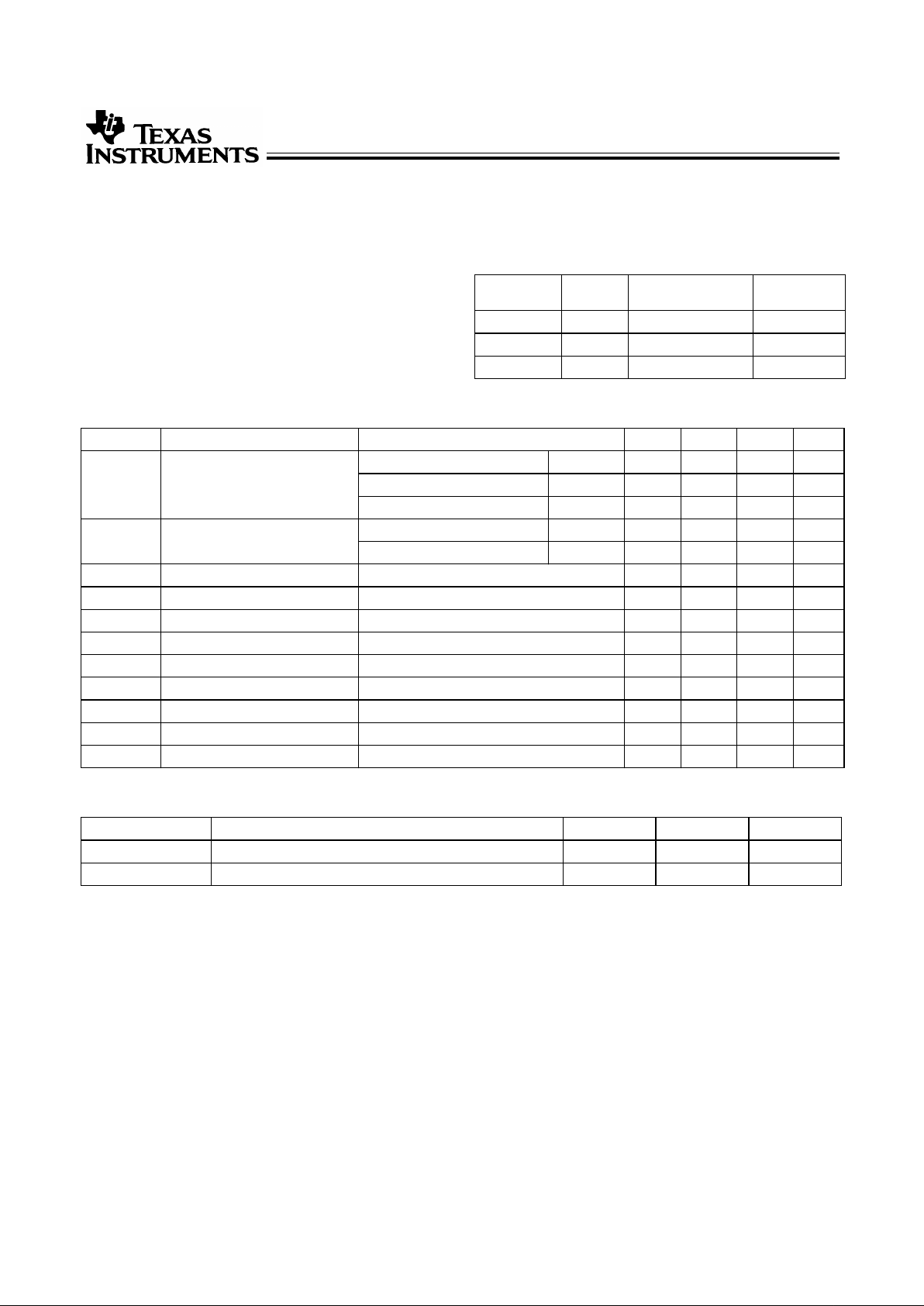
Electrical Characteristics Over the Operating Range
Parameter Description Test Conditions Min. Typ.
[5]
Max. Unit
V
OH
Output HIGH Voltage V
CC
=Min., I
OH
=−32 mA Com’l 2.0 V
V
CC
=Min., I
OH
=−15 mA Com’l 2.4 3.3 V
V
CC
=Min., I
OH
=−12 mA Mil 2.4 3.3 V
V
OL
Output LOW Voltage V
CC
=Min., I
OL
=64 mA Com’l 0.3 0.55 V
V
CC
=Min., I
OL
=48mA Mil 0.3 0.55 V
V
IH
Input HIGH Voltage 2.0 V
V
IL
Input LOW Voltage 0.8 V
V
H
Hysteresis
[6]
All inputs 0.2 V
V
IK
Input Clamp Diode Voltage V
CC
=Min., I
IN
=−18 mA −0.7 −1.2 V
I
I
Input HIGH Current V
CC
=Max., V
IN
=V
CC
5 µA
I
IH
Input HIGH Current V
CC
=Max., V
IN
=2.7V ±1 µA
I
IL
Input LOW Current V
CC
=Max., V
IN
=0.5V ±1 µA
I
OS
Output Short Circuit Current
[7]
V
CC
=Max., V
OUT
=0.0V −60 −120 −225 mA
I
OFF
Power-Off Disable V
CC
=0V, V
OUT
=4.5V ±1 µA
Capacitance
[6]
Parameter Description Typ.
[5]
Max. Unit
C
IN
Input Capacitance 5 10 pF
C
OUT
Output Capacitance 9 12 pF
Notes:
2. Unless otherwise noted, these limits are over the operating free-air temperature range.
3. Unused inputs must always be connected to an appropriate logic voltage level, preferably either V
CC
or ground.
4. T
A
is the “instant on” case temperature.
5. Typical values are at V
CC
=5.0V, T
A
=+25˚C ambient.
6. This parameter is specified but not tested.
7. Not morethan one output shouldbe shorted at a time.Duration of short should notexceed one second.The use of high-speedtest apparatus and/or sample
and holdtechniques are preferablein order tominimize internal chip heatingand more accurately reflect operational values.Otherwise prolonged shorting of
a high output mayraise the chip temperature well abovenormal and thereby cause invalid readings in other parametric tests. In any sequence of parameter
tests, I
OS
tests should be performed last.
CY54/74FCT245T
3
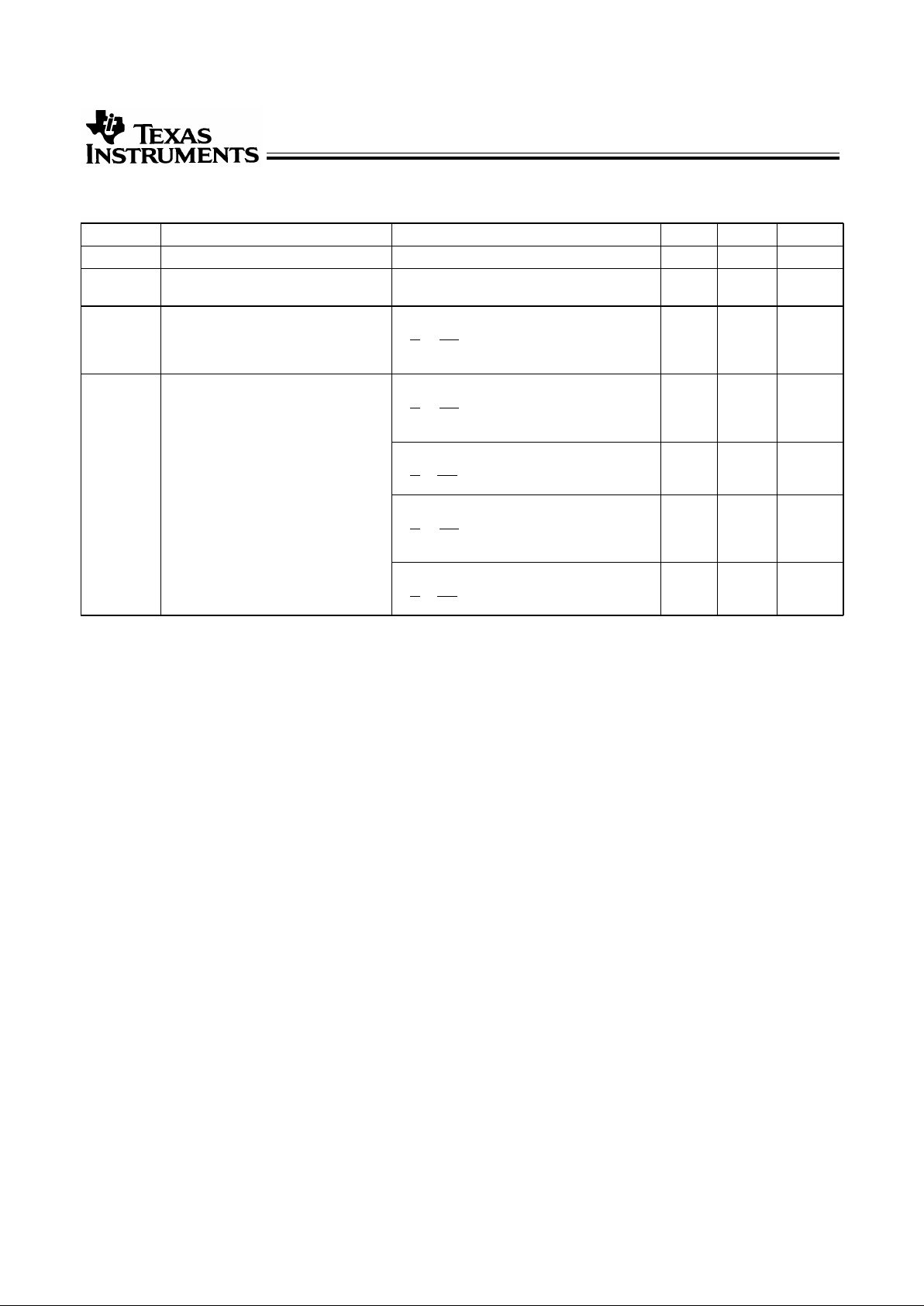
Power Supply Characteristics
Parameter Description Test Conditions Typ.
[5]
Max. Unit
I
CC
Quiescent Power Supply Current V
CC
=Max., V
IN
≤0.2V, V
IN
≥V
CC
−0.2V 0.1 0.2 mA
∆I
CC
Quiescent Power Supply Current
(TTL inputs HIGH)
V
CC
=Max., V
IN
=3.4V,
[8]
f
1
=0, Outputs Open
0.5 2.0 mA
I
CCD
Dynamic Power Supply Current
[9]
V
CC
=Max., One Input Toggling,
50% Duty Cycle, Outputs Open,
T/
R or OE=GND and
V
IN
≤0.2V or V
IN
≥V
CC
−0.2V
0.06 0.12 mA/MHz
I
C
Total Power Supply Current
[10]
V
CC
=Max.,50% DutyCycle,OutputsOpen,
One Bit Toggling at f
1
=10 MHz,
T/
R or OE=GND and
V
IN
≤0.2V or V
IN
≥V
CC
−0.2V
0.7 1.4 mA
V
CC
=Max.,50% DutyCycle,OutputsOpen,
One Bit Toggling at f
1
=10 MHz,
T/
RorOE=GND and V
IN
=3.4VorV
IN
=GND
1.2 3.4 mA
V
CC
=Max.,50% DutyCycle,OutputsOpen,
Eight Bits Toggling at f
1
=2.5 MHz,
T/
R or OE=GND and
V
IN
≤0.2V or V
IN
≥V
CC
−0.2V
1.3 2.6
[11]
mA
V
CC
=Max.,50% DutyCycle,OutputsOpen,
Eight Bits Toggling at f
1
=2.5 MHz,
T/
RorOE=GND and V
IN
=3.4VorV
IN
=GND
3.3 10.6
[11]
mA
Notes:
8. Per TTL driven input (V
IN
=3.4V); all other inputs at V
CC
or GND.
9. This parameter is not directly testable, but is derived for use in Total Power Supply calculations.
10. I
C
=I
QUIESCENT
+ I
INPUTS
+ I
DYNAMIC
I
C
=I
CC
+∆I
CC
D
H
N
T
+I
CCD
(f
0
/2 + f
1
N
1
)
I
CC
= Quiescent Current with CMOS input levels
∆I
CC
= Power Supply Current for a TTL HIGH input (V
IN
=3.4V)
D
H
= Duty Cycle for TTL inputs HIGH
N
T
= Number of TTL inputs at D
H
I
CCD
= Dynamic Current caused by an input transition pair (HLH or LHL)
f
0
= Clock frequency for registered devices, otherwise zero
f
1
= Input signal frequency
N
1
= Number of inputs changing at f
1
All currents are in milliamps and all frequencies are in megahertz.
11. Values for these conditions are examples of the I
CC
formula. These limits are specified but not tested.
 Loading...