


CD74HCT4351E
Texas Instruments CD74HCT4351E, CD74HC4352E, CD74HC4351M96, CD74HC4351M, CD74HC4351E Datasheet
...
Data sheet acquired from Harris Semiconductor
/
j
/
/
SCHS213
September 1998
CD74HC4351,
CD74HCT4351, CD74HC4352
High Speed CMOS Logic
Analog Multiplexers/Demultiplexers with Latch
[ /Title
(CD74
HC435
1,
CD74
HCT43
51,
CD74
HC435
2)
Subect
(High
Speed
CMOS
Logic
Analog
Multiplexers/De
multiplexers
with
Latch)
Autho
r ()
Key-
words
(High
Speed
CMOS
Logic
Features
• Wide Analog Input Voltage Range . . . . . . . . . ±5V (Max)
• Low “On” Resistance
-V
- VEE = 4.5V. . . . . . . . . . . . . . . . . . . . . .70Ω (Typ)
CC
-V
- VEE = 9V . . . . . . . . . . . . . . . . . . . . . . .40Ω (Typ)
CC
• Low Crosstalk Between Switches
• Fast Switching and Propagation Speeds
• “Break-Before-Make” Switching
o
• Wide Operating Temperature Range . . . -55
C to 125oC
• HC Types
- 2V to 6V Operation, Control; 0V to 10V Switch
- High Noise Immunity: N
= 30%, NIH = 30% of V
IL
CC
at VCC = 5V
• HCT Types
- 4.5V to 5.5V Operation, Control; 0V to 10V Switch
- Direct LSTTL Input Logic Compatibility,
V
= 0.8V (Max), VIH = 2V (Min)
IL
- CMOS Input Compatibility, I
≤ 1µA at VOL, V
l
OH
Pinouts
CD74HC4351, CD74HCT4351
(PDIP, SOIC)
TOP VIEW
A4
A6
NC
A COMMON
A7
A5
E1
E2
V
EE
GND
1
2
3
4
5
6
7
8
9
10
V
20
CC
A2
19
A1
18
A0
17
A3
16
S0
15
NC
14
S1
13
12
S2
11
LE 11
Description
The Harris CD74HC4351, CD74HCT4351 and
CD74HC4352 are digitally controlled analog switches which
utilize silicon-gate CMOS technology to achieve operating
speeds similar to LSTTL with the low power consumption of
standard CMOS integrated circuits.
These analog multiplexers/demultiplexers are, in essence,
the HC/HCT4015 and HC4052 preceded by address latches
that are controlled by an active low Latch Enable input (
Two Enable inputs, one active low (
E1), and the other active
LE).
high (E2) are provided allowing enabling with either input
voltage level.
Ordering Information
PKG.
PART NUMBER TEMP. RANGE (oC) PACKAGE
CD74HC4351E -55 to 125 20 Ld PDIP E20.3
CD74HCT4351E -55 to 125 20 Ld PDIP E20.3
CD74HC4352E -55 to 125 20 Ld PDIP E20.3
CD74HC4351M -55 to 125 20 Ld SOIC M20.15
NOTES:
1. When ordering, use the entire part number.Add the suffix 96 to
obtain the variant in the tape and reel.
2. Wafer and die for this part number is available which meets all
electrical specifications. Please contact your local sales office or
Harris customer service for ordering information.
CD74HC4352
(PDIP)
TOP VIEW
B0
B2
NC
B COMMON
B3
B1
E1
E2
V
EE
GND
1
2
3
4
5
6
7
8
9
10
V
20
CC
A2
19
A1
18
A COMMON
17
A0
16
A3
15
NC
14
S0
13
12
S1
LE
NO.
CAUTION: These devices are sensitive to electrostatic discharge. Users should follow proper IC Handling Procedures.
Copyright
© Harris Corporation 1998
1
File Number 2145.2

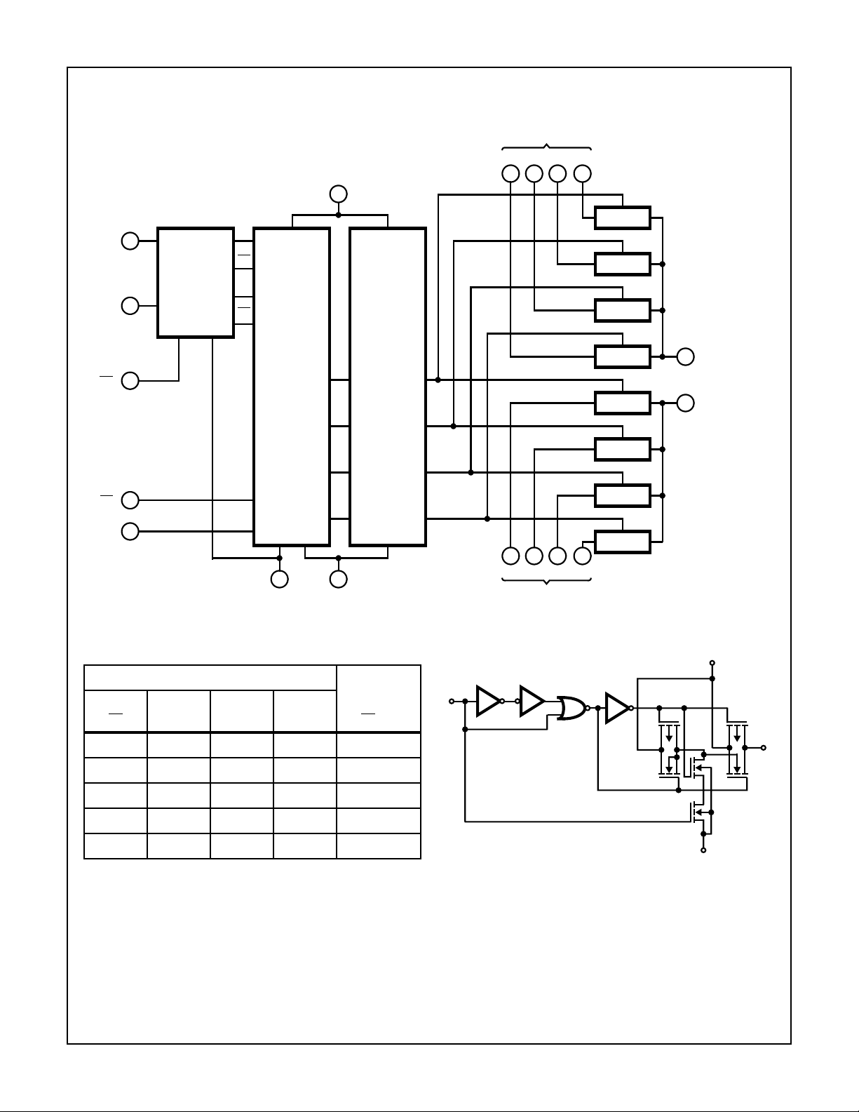
Functional Diagram
CD74HC4351, CD74HCT4351, CD74HC4352
CD74HC4351, CD74HCT4351
S0
S1
S2
V
CC
20
15
13
12
11LE
7E1
8E2
LATCHES
LOGIC
LEVEL
CONVERSION
BINARY
TO
1 OF 8
DECODER
WITH
ENABLE
A
CHANNEL IN/OUT
7A6A5A4A3A2A1A0
171819161625
TG
TG
TG
TG
TG
TG
TG
TG
4
A
COMMON
OUT/IN
10 9
GND V
EE
TRUTH TABLE
CD74HC4351, CD74HCT4351
INPUT STATES (NOTE 3)
“ON”
SWITCHES
LE = HE1 E2 S2 S1 S0
LHLLL A
LHLLH A
LHLHL A
LHLHH A
LHHLL A
LHHLH A
LHHHL A
LHHHH A
H L X X X None
NOTE:
3. When LE is low S0-S2 data are latched and switches cannot
change state.
H = High Voltage Level, L = Low Voltage Level, X = Don’t Care
0
1
2
3
4
5
6
7
FROM
SELECT
LOGIC
V
CC
N
FIGURE 1. DETAIL OF ONE HC/HCT4351 SWITCH
An
IN/OUT
P
N
V
EE
P
V
CC
A COMMON
IN/OUT
N
N
2
Functional Diagram
13
S0
LATCHES
12
S1
11LE
CD74HC4351, CD74HCT4351, CD74HC4352
CD74HC4352
A CHANNELS IN/OUT
A3A2A1A
V
CC
20
S0
S0
S1
S1
BINARY
LOGIC
LEVEL
CONVERSION
TO
1 OF 4
DECODER
WITH
ENABLE
0
16181915
TG
TG
TG
A COMMON
TG
TG
TG
17
4
OUT/IN
B COMMON
OUT/IN
7E1
8E2
10 9
GND V
EE
TRUTH TABLE
CD74HC4352
INPUT STATES (NOTE 4)
“ON”
SWITCHES
LE = HE1 E2 S1 S0
LHLLA
LHLHA
LHHLA
LHHHA
, B
0
0
, B
1
1
, B
2
2
, B
3
3
H L X X None
NOTE:
4. When Latch Enable is “Low” channel-select data is latched and
switches cannot change state.
H = High Voltage Level, L = Low Voltage Level, X = Don’t Care
TG
TG
1625
B
FROM
SELECT
LOGIC
B
0
B CHANNELS IN/OUT
B
1
3B2
V
CC
N
FIGURE 2. DETAIL OF ONE CD74HC4352 SWITCH
An (Bn)
IN/OUT
P
N
V
EE
P
V
CC
A COMMON (B COMMON)
IN/OUT
N
N
3
CD74HC4351, CD74HCT4351, CD74HC4352
Absolute Maximum Ratings Thermal Information
DC Supply Voltage, VCC. . . . . . . . . . . . . . . . . . . . . . . . -0.5V to 7V
DC Supply Voltage, V
CC - VEE
. . . . . . . . . . . . . . . . . . -0.5V to 10.5V
DC Supply Voltage, VEE . . . . . . . . . . . . . . . . . . . . . . . . 0.5V to -7V
DC Input Diode Current, I
IK
For VI < -0.5V or VI > VCC 0.5V. . . . . . . . . . . . . . . . . . . . . . . .±20mA
DC Switch Diode Current, I
OK
For VI < VEE -0.5V or VI < VCC + 0.5V . . . . . . . . . . . . . . . . .±25mA
DC Switch Current, IOK (Note 5)
For VI > VEE -0.5V or VI < VCC + 0.5V . . . . . . . . . . . . . . . . .±20mA
DC Output Diode Current, I
OK
For VO < -0.5V or VO > VCC + 0.5V . . . . . . . . . . . . . . . . . . . .±20mA
DC Output Source or Sink Current per Output Pin, I
O
For VO > -0.5V or VO < VCC + 0.5V . . . . . . . . . . . . . . . . . . . .±25mA
DC VCC or Ground Current, ICC . . . . . . . . . . . . . . . . . . . . . . . . .±50mA
Operating Conditions
Temperature Range, TA . . . . . . . . . . . . . . . . . . . . . . -55oC to 125oC
Supply Voltage Range, V
HC Types . . . . . . . . . . . . . . . . . . . . . . . . . . . . . . . . . . . . .2V to 6V
HCT Types . . . . . . . . . . . . . . . . . . . . . . . . . . . . . . . . .4.5V to 5.5V
Supply Voltage Range, V
HC, HCT Types (Figure 3) . . . . . . . . . . . . . . . . . . . . . . .2V to 10V
Supply Voltage Range, V
HC, HCT Types (Figure 4) . . . . . . . . . . . . . . . . . . . . . . . 0V to -6V
DC Input or Output Voltage, VI. . . . . . . . . . . . . . . . . . . GND to V
Analog Switch I/O Voltage, VIS. . . . . . . . . . . . . . . . . . . . . VEE (Min)
. . . . . . . . . . . . . . . . . . . . . . . . . . . . . . . . . . . . . . . . . . .VCC (Max)
Input Rise and Fall Time, tr, t
2V . . . . . . . . . . . . . . . . . . . . . . . . . . . . . . . . . . . . . . 1000ns (Max)
4.5V. . . . . . . . . . . . . . . . . . . . . . . . . . . . . . . . . . . . . . 500ns (Max)
6V . . . . . . . . . . . . . . . . . . . . . . . . . . . . . . . . . . . . . . . 400ns (Max)
CAUTION: Stresses above those listed in “Absolute Maximum Ratings” may cause permanent damage to the device. This is a stress only rating and operation
of the device at these or any other conditions above those indicated in the operational sections of this specification is not implied.
NOTES:
5. In certain applications, the external load-resistor current may include both VCCandsignal-linecomponents.ToavoiddrawingVCCcurrent
when switch current flows into the transmission gate inputs, the voltage drop across the bidirectional switch must not exceed 0.6V (calculated from RONvalues shown in the DC Electrical Specifications table). No VCCcurrent will flow through RLif the switch current flows
into terminal 3 on the HC/HCT4351; terminals 3 and 13 on the HC4352.
6. θJA is measured with the component mounted on an evaluation PC board in free air.
CC
CC -VEE
EE
f
Thermal Resistance (Typical, Note 6) θJA (oC/W)
PDIP Package. . . . . . . . . . . . . . . . . . . . . . . . . . . . . 125
SOIC Package. . . . . . . . . . . . . . . . . . . . . . . . . . . . . 120
Maximum Junction Temperature . . . . . . . . . . . . . . . . . . . . . . . 150oC
Maximum Storage Temperature Range . . . . . . . . . .-65oC to 150oC
Maximum Lead Temperature (Soldering 10s). . . . . . . . . . . . . 300oC
(SOIC - Lead Tips Only)
CC
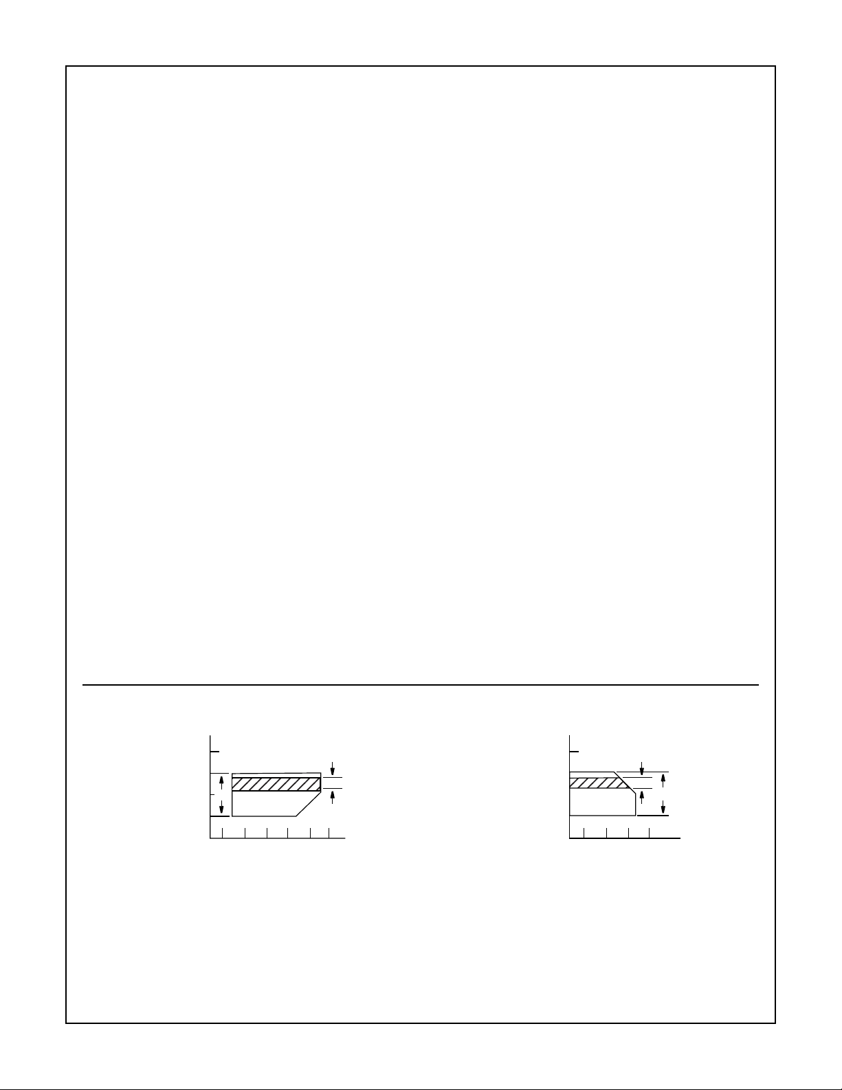
Recommended Operating Area as a Function of Supply Voltage
8
(V)
6
HC
4
2
0
024681012
V
- VEE (V)
CC
HCT
FIGURE 3. FIGURE 4.
4
VCC - GND
VCC - GND
(V)
8
6
4
2
0
0-2-4-6-8
V
EE
HCT
- GND (V)
HC
CD74HC4351, CD74HCT4351, CD74HC4352
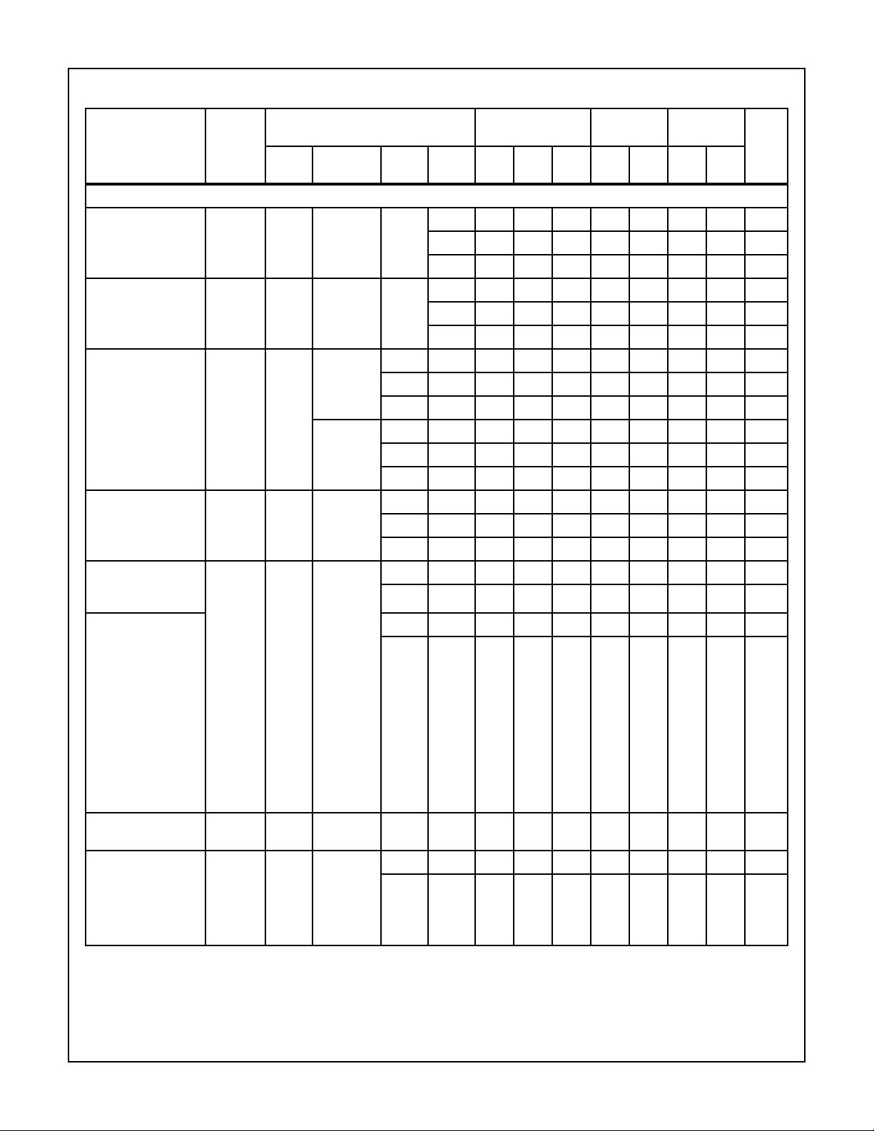
DC Electrical Specifications
PARAMETER SYMBOL
HC TYPES
High Level Input
Voltage
Low Level Input
Voltage
“ON” Resistance
I
= 1mA
O
Figure 9
Maximum “ON”
Resistance Between
Any Two Channels
Switch On/Off
Leakage Current
4 Channels (4352)
Switch On/Off
Leakage Current
8 Channels (4351)
Control Input Leakage
Current
Quiescent Device
Current
I
= 0
O
R
∆R
V
V
I
ON
I
IZ
I
IL
CC
IH
IL
ON
TEST CONDITIONS 25
(V) VIS(V)
I
V
(V)
EE
V
CC
(V) MIN TYP MAX MIN MAX MIN MAX
o
C
-40oC TO
85oC
-55oC TO
125oC
UNITSV
- - - 2 1.5 - - 1.5 - 1.5 - V
4.5 3.15 - - 3.15 - 3.15 - V
6 4.2 - - 4.2 - 4.2 - V
- - - 2 - - 0.5 - 0.5 - 0.5 V
4.5 - - 1.35 - 1.35 - 1.35 V
6 - - 1.8 - 1.8 - 1.8 V
VIH or
VCCor V
V
IL
0 4.5 - 70 160 - 200 - 240 Ω
EE
0 6 - 60 140 - 175 - 210 Ω
-4.5 4.5 - 40 120 - 150 - 180 Ω
V
CC
to V
0 4.5 - 90 180 - 225 - 270 Ω
EE
0 6 - 80 160 - 200 - 240 Ω
-4.5 4.5 - 45 130 - 162 - 195 Ω
- - 04.5-10-----Ω
0 6 -8.5-----Ω
-4.5 4.5 - 5 -----Ω
VIH or
V
IL
For Switch
OFF:
When
VIS = V
CC
VOS=VEE;
When
VIS = VEE,
VOS = V
CC
06--±0.1 - ±1-±1µA
-5 5 - - ±0.2 - ±2-±2µA
06--±0.2 - ±2-±2µA
-5 5 - - ±0.4 - ±4-±4µA
For Switch
ON:
All
Applicable
Combina-
tions of V
and V
IS
OS
Voltage
Levels
VCCor
-06--±0.1 - ±1-±1µA
GND
VCCor
GND
When
VIS = VEE,
VOS=VCC,
0 6 - - 8 - 80 - 160 µA
-5 5 - - 16 - 160 - 320 µA
When
VIS = VCC,
VOS = V
EE
5
 Loading...