


Texas Instruments CD74HCT40105M96, CD74HCT40105M, CD74HCT40105E, CD74HC40105M, CD74HC40105E Datasheet
...[ /Title (CD74 HC401 05, CD74 HCT40 105) /Subject (High Speed CMOS
Data sheet acquired from Harris Semiconductor SCHS222
February 1998
CD74HC40105,
CD74HCT40105
High Speed CMOS Logic
4-Bit x 16-Word FIFO Register
Features
•Independent Asynchronous Inputs and Outputs
•Expandable in Either Direction
•Reset Capability
•Status Indicators on Inputs and Outputs
•Three-State Outputs
•Shift-Out Independent of Three-State Control
•Fanout (Over Temperature Range)
-Standard Outputs . . . . . . . . . . . . . . . 10 LSTTL Loads
-Bus Driver Outputs . . . . . . . . . . . . . 15 LSTTL Loads
•Wide Operating Temperature Range . . . -55oC to 125oC
•Balanced Propagation Delay and Transition Times
•Significant Power Reduction Compared to LSTTL Logic ICs
•HC Types
-2V to 6V Operation
-High Noise Immunity: NIL = 30%, NIH = 30% of VCC at VCC = 5V
•HCT Types
-4.5V to 5.5V Operation
-Direct LSTTL Input Logic Compatibility, VIL= 0.8V (Max), VIH = 2V (Min)
-CMOS Input Compatibility, Il ≤ 1μA at VOL, VOH
Applications
•Bit-Rate Smoothing
•CPU/Terminal Buffering
•Data Communications
•Peripheral Buffering
•Line Printer Input Buffers
•Auto-Dialers
•CRT Buffer Memories
•Radar Data Acquisition
Description
The Harris CD74HC40105 and CD74HCT40105 are highspeed silicon-gate CMOS devices that are compatible, except for “shift-out” circuitry, with the Harris CD40105B. They are low-power first-in-out (FIFO) “elastic” storage registers that can store 16 four-bit words. The 40105 is capable of handling input and output data at different shifting rates. This feature makes particularly useful as a buffer between asynchronous systems.
Each work position in the register is clocked by a control flipflop, which stores a marker bit. A “1” signifies that the position’s data is filled and a “0” denotes a vacancy in that position. The control flip-flop detects the state of the preceding flip-flop and communicates its own status to the succeeding flip-flop. When a control flip-flop is in the “0” state and sees a “1” in the preceeding flip-flop, it generates a clock pulse that transfers data from the preceding four data latches into its own four data latches and resets the preceding flip-flop to “0”. The first and last control flip-flops have buffered outputs. Since all empty locations “bubble” automatically to the input end, and all valid data ripple through to the output end, the status of the first control flip-flop (DATA-IN READY) indicates if the FIFO is full, and the status of the last flip-flop (DATAOUT READY) indicates if the FIFO contains data. As the earliest data are removed from the bottom of the data stack (the output end), all data entered later will automatically propagate (ripple) toward the output.
Ordering Information
|
TEMP. RANGE |
|
|
PART NUMBER |
(oC) |
PACKAGE |
PKG. NO. |
CD74HC40105E |
-55 to 125 |
16 Ld PDIP |
E16.3 |
|
|
|
|
CD74HCT40105E |
-55 to 125 |
16 Ld PDIP |
E16.3 |
|
|
|
|
CD74HC40105M |
-55 to 125 |
16 Ld SOIC |
M16.15 |
|
|
|
|
CD74HCT40105M |
-55 to 125 |
16 Ld SOIC |
M16.15 |
|
|
|
|
NOTES: |
|
|
|
1.When ordering, use the entire part number. Add the suffix 96 to obtain the variant in the tape and reel.
2.Wafer and die for this part number is available which meets all electrical specifications. Please contact your local sales office or Harris customer service for ordering information.
CAUTION: These devices are sensitive to electrostatic discharge. Users should follow proper IC Handling Procedures. |
File Number 1834.1 |
|
|
||
Copyright © Harris Corporation 1998 |
1 |
|
|
|
|
CD74HC40105, CD74HCT40105
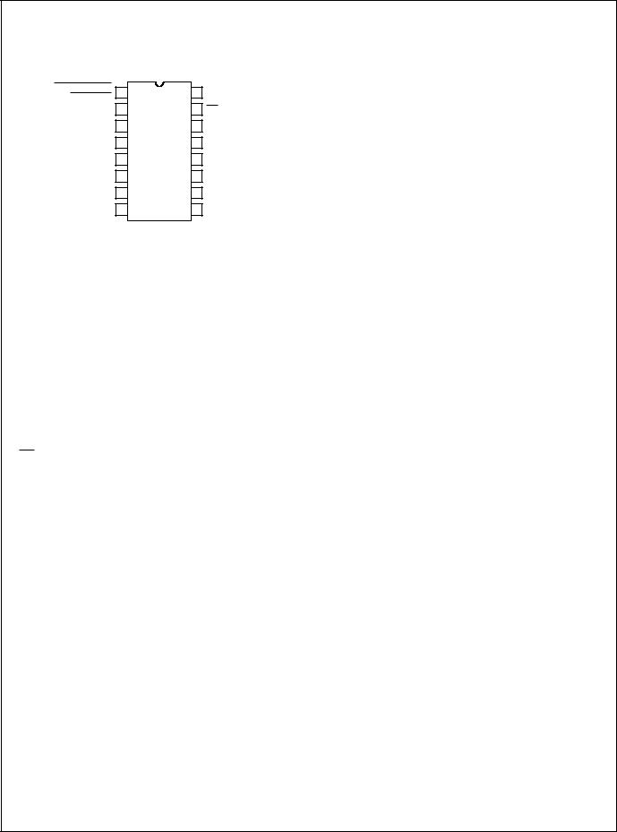
Pinout
CD74HC40105, CD74HCT40105
(PDIP, SOIC)
TOP VIEW
THREE-STATE |
1 |
16 VCC |
CONTROL |
DIR |
2 |
15 SO |
SI |
3 |
14 DOR |
D0 |
4 |
13 |
Q0 |
D1 |
5 |
12 |
Q1 |
D2 |
6 |
11 |
Q2 |
D3 |
7 |
10 |
Q3 |
GND |
8 |
9 |
MR |
Loading Data
Data can be entered whenever the DATA-IN READY (DIR) flag is high, by a low to high transition on the SHIFT-IN (SI) input. This input must go low momentarily before the next word is accepted by the FIFO. The DIR flag will go low momentarily, until the data have been transferred to the second location. The flag will remain low when all 16-word locations are filled with valid data, and further pulses on the SI input will be ignored until DIR goes high.
Unloading Data
As soon as the first word has rippled to the output, the dataout ready output (DOR) goes HIGH and data of the first word is available on the outputs. Data of other words can be removed by a negative-going transition on the shift-out input (SO). This negative-going transition causes the DOR signal to go LOW while the next word moves to the output. As long as valid data is available in the FIFO, the DOR signal will go high again, signifying that the next word is ready at the output. When the FIFO is empty, DOR will remain LOW, and any further commands will be ignored until a “1” marker ripples down to the last control register and DOR goes HIGH. If during unloading SI is HIGH, (FIFO is full) data on the data input of the FIFO is entered in the first location.
Master Reset
A high on the MASTER RESET (MR) sets all the control logic marker bits to “0”. DOR goes low and DIR goes high. The contents of the data register are not changed, only declared invalid, and will be superseded when the first word is loaded. Thus, MR does not clear data within the register but only the control logic. If the shift-in flag (SI) is HIGH during the master reset pulse, data present at the input (D0 to D3) are immediately moved into the first location upon completion of the reset process.
Three-State Outputs
In order to facilitate data busing, three-state outputs (Q0 to Q3) are provided on the data output lines, while the load condition of the register can be detected by the state of the DOR output. A HIGH on the three-state control flag (output enable input OE) forces the outputs into the high-impedance OFF-state mode. Note that the shift-out signal, unlike that in the Harris CD40105B, is independent of the three-state output control. In the CD40105B, the three-state control must not be shifted from High to Low when the shift-out signal is Low (data loss would occur). In the high-speed CMOS version this restriction has been eliminated.
Cascading
The 40105 can be cascaded to form longer registers simply by connecting the DIR to SO and DOR to SI. In the cascaded mode, a MASTER RESET pulse must be applied after the supply voltage is turned on. For words wider than four bits, the DIR and the DOR outputs must be gated together with AND gates. Theri outputs drive the SI and SO inputs in parallel, if expanding is done in both directions (see Figures 12 and 13).
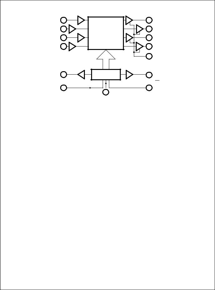
Functional Diagram
|
|
THREE- |
|
|
|
|
|
|
|||||||
|
|
|
STATE |
|
|
|
|
|
|
|
|
||||
|
|
|
|
|
|
|
|
|
1 |
|
|
|
|
||
|
CONTROL |
|
13 |
|
|||||||||||
|
|
|
|
||||||||||||
4 |
|
|
Q0 |
||||||||||||
|
|
|
D0 |
|
|
|
|
|
|
|
|
||||
|
|
|
|
|
|
12 |
|
||||||||
|
|
|
|
|
|
||||||||||
5 |
|
|
Q1 |
||||||||||||
|
|
|
D1 |
|
|
|
|
|
|
||||||
|
|
|
|
|
|
|
11 |
||||||||
|
|
|
|
|
|
|
|
||||||||
6 |
|
|
Q2 |
||||||||||||
|
|
|
|
||||||||||||
|
|
|
D2 |
|
|
|
|
|
|
|
10 |
||||
|
|
|
|
|
|
|
|
|
|||||||
7 |
|
|
Q3 |
||||||||||||
|
|
|
D3 |
|
|
|
|
|
|
|
|||||
|
|
|
|
|
|
|
|||||||||
|
|
|
|
|
|
|
|||||||||
3 |
|
|
14 |
DATA-OUT |
|||||||||||
|
SHIFT IN |
|
|
|
|
|
|
|
READY |
||||||
15 |
|
|
2 |
||||||||||||
|
|
|
|
|
|
|
|
|
|
||||||
|
|
|
|
|
DATA-IN |
||||||||||
SHIFT OUT |
|
|
|||||||||||||
|
|
|
|
|
|
|
|||||||||
|
|
|
|
|
|
|
|
|
|
|
|
|
|
|
READY |
|
MASTER |
9 |
GND = 8 |
|
|||||||||||
|
|
VCC = 16 |
|
||||||||||||
|
RESET |
|
|
|
|||||||||||
2
CD74HC40105, CD74HCT40105
|
|
INPUT |
OUTPUT |
|
|
|
BUFFERS |
BUFFERS |
|
D0 |
4 |
|
13 |
Q0 |
D1 |
5 |
4 x 16 |
12 |
Q1 |
|
|
DATA |
|
|
D2 |
6 |
REGISTER |
11 |
Q2 |
|
||||
D3 |
7 |
|
10 |
Q3 |
|
|
|
1 |
|
THREE-STATE CONTROL
DATA-OUT READY (DOR)
DATA-IN READY (DIR)
2 |
CONTROL LOGIC |
14 |
|
|
SHIFT OUT (SO) |
3 |
|
15 |
9
SHIFT IN (SI)
MASTER
RESET (MR)
FIGURE 1. FUNCTIONAL BLOCK DIAGRAM
3

|
|
|
CD74HC40105, CD74HCT40105 |
|
|
|
|
|
||
|
9 |
|
|
|
|
|
|
|
|
|
|
MR |
|
|
|
|
|
|
|
|
|
|
|
|
|
|
|
|
|
|
|
14 |
|
|
|
|
|
|
|
|
|
|
DOR |
|
3 |
|
|
|
|
|
|
|
|
|
|
SI |
|
|
|
|
|
|
|
|
15 |
|
|
|
|
|
F/Fs |
|
|
F/F16 |
|
S0 |
|
|
|
F/F1 |
|
2-15 |
|
|
|
|
|
|
|
R Q |
|
|
|
|
|
|
||
|
|
R Q |
|
R Q |
|
|
R Q |
|
|
|
|
|
† |
|
|
|
|
|
|||
|
|
† † |
|
† † |
|
|
† † |
|
|
|
|
|
S Q |
|
|
|
|
|
|||
|
|
S Q |
|
S Q |
|
|
S Q |
|
|
|
|
|
|
|
|
|
|
|
|||
|
|
|
|
|
|
|
|
|
R |
|
|
|
|
|
|
|
|
|
|
|
† |
|
2 |
|
|
|
14 x |
|
|
|
S |
Q |
|
|
|
|
|
|
|
|
|
|
|
DIR |
|
|
|
|
|
|
|
|
|
|
|
|
|
|
|
14 x |
|
|
|
|
|
|
4 |
|
|
|
|
|
|
|
|
13 |
|
D0 |
CL |
CL |
CL |
CL |
CL |
CL |
|
|
Q0 |
|
|
|
|
|
||||||
|
5 |
|
|
|
|
|
|
|
|
12 |
|
|
|
|
|
|
|
|
THREE- |
||
|
D1 |
|
|
|
|
|
|
Q1 |
||
|
|
|
4 |
4 x 14 |
|
4 |
STATE |
|
|
|
|
6 |
LATCHES |
LATCHES |
LATCHES |
OUTPUT |
11 |
||||
|
D2 |
|
|
|
|
|
|
BUFFERS |
Q2 |
|
|
7 |
|
L1 |
14 x L1 |
|
L16 |
E |
E |
10 |
|
|
D3 |
|
|
Q3 |
||||||
|
|
|
|
|
|
|
|
|
||
|
|
POSITION 1 |
POSITION 2-15 |
POSITIONS 16 |
|
|
|
|||
|
|
|
1 |
|
|
|
|
|
|
|
|
|
|
OE |
|
|
|
|
|
|
|
† |
“S” overrides “R”. |
|
|
|
|
|
|
|
|
|
†† |
“R” overrides “S”. |
|
|
|
|
|
|
|
|
|
|
|
|
FIGURE 2. LOGIC DIAGRAM |
|
|
|
|
|
||
|
|
|
|
4 |
|
|
|
|
|
|

CD74HC40105, CD74HCT40105
Absolute Maximum Ratings
DC Supply Voltage, VCC . . . . . . . . . . . . . . . . . . . . . . . . |
-0.5V to 7V |
DC Input Diode Current, IIK |
±20mA |
For VI < -0.5V or VI > VCC + 0.5V . . . . . . . . . . . . . . . . . . |
|
DC Output Diode Current, IOK |
±20mA |
For VO < -0.5V or VO > VCC + 0.5V . . . . . . . . . . . . . . . . |
|
DC Output Source or Sink Current per Output Pin, IO |
±25mA |
For VO > -0.5V or VO < VCC + 0.5V . . . . . . . . . . . . . . . . |
|
DC VCC or Ground Current, ICC . . . . . . . . . . . . . . . . . . . . . |
. . . .±50mA |
Thermal Information |
|
Thermal Resistance (Typical, Note 3) |
θJA (oC/W) |
PDIP Package . . . . . . . . . . . . . . . . . . . . . . . . . . . . |
. 90 |
SOIC Package . . . . . . . . . . . . . . . . . . . . . . . . . . . . |
. 160 |
Maximum Junction Temperature . . . . . . . . . . . . . . . . |
. . . . . . . 150oC |
Maximum Storage Temperature Range . . . . . . . . . . |
-65oC to 150oC |
Maximum Lead Temperature (Soldering 10s) . . . . . . |
. . . . . . . 300oC |
(SOIC - Lead Tips Only) |
|
Operating Conditions
Temperature Range (TA) . . . . . . . . . . . . . . . . . . . . . -55oC to 125oC Supply Voltage Range, VCC
HC Types . . . . . . . . . . . . . . . . . . . . . . . . . . . . . . . . . . . . .2V to 6V HCT Types . . . . . . . . . . . . . . . . . . . . . . . . . . . . . . . . .4.5V to 5.5V
DC Input or Output Voltage, VI, VO . . . . . . . . . . . . . . . . . 0V to VCC Input Rise and Fall Time
2V . . . . . . . . . . . . . . . . . . . . . . . . . . . . . . . . . . . . . . 1000ns (Max) 4.5V. . . . . . . . . . . . . . . . . . . . . . . . . . . . . . . . . . . . . . 500ns (Max) 6V . . . . . . . . . . . . . . . . . . . . . . . . . . . . . . . . . . . . . . . 400ns (Max)
CAUTION: Stresses above those listed in “Absolute Maximum Ratings” may cause permanent damage to the device. This is a stress only rating and operation of the device at these or any other conditions above those indicated in the operational sections of this specification is not implied.
NOTE:
3. θJA is measured with the component mounted on an evaluation PC board in free air.
DC Electrical Specifications
|
|
TEST |
|
|
25oC |
|
-40oC TO 85oC |
-55oC TO 125oC |
|
|||
|
|
CONDITIONS |
VCC |
|
|
|
||||||
PARAMETER |
SYMBOL |
VI (V) |
IO (mA) |
(V) |
MIN |
TYP |
MAX |
MIN |
MAX |
MIN |
MAX |
UNITS |
HC TYPES |
|
|
|
|
|
|
|
|
|
|
|
|
|
|
|
|
|
|
|
|
|
|
|
|
|
High Level Input |
VIH |
- |
- |
2 |
1.5 |
- |
- |
1.5 |
- |
1.5 |
- |
V |
Voltage |
|
|
|
|
|
|
|
|
|
|
|
|
|
|
|
4.5 |
3.15 |
- |
- |
3.15 |
- |
3.15 |
- |
V |
|
|
|
|
|
|||||||||
|
|
|
|
|
|
|
|
|
|
|
|
|
|
|
|
|
6 |
4.2 |
- |
- |
4.2 |
- |
4.2 |
- |
V |
|
|
|
|
|
|
|
|
|
|
|
|
|
Low Level Input |
VIL |
- |
- |
2 |
- |
- |
0.5 |
- |
0.5 |
- |
0.5 |
V |
Voltage |
|
|
|
|
|
|
|
|
|
|
|
|
|
|
|
4.5 |
- |
- |
1.35 |
- |
1.35 |
- |
1.35 |
V |
|
|
|
|
|
|||||||||
|
|
|
|
|
|
|
|
|
|
|
|
|
|
|
|
|
6 |
- |
- |
1.8 |
- |
1.8 |
- |
1.8 |
V |
|
|
|
|
|
|
|
|
|
|
|
|
|
High Level Output |
VOH |
VIH or VIL |
-0.02 |
2 |
1.9 |
- |
- |
1.9 |
- |
1.9 |
- |
V |
Voltage |
|
|
|
|
|
|
|
|
|
|
|
|
|
|
-0.02 |
4.5 |
4.4 |
- |
- |
4.4 |
- |
4.4 |
- |
V |
|
CMOS Loads |
|
|
||||||||||
|
|
|
|
|
|
|
|
|
|
|
|
|
|
|
-0.02 |
6 |
5.9 |
- |
- |
5.9 |
- |
5.9 |
- |
V |
|
|
|
|
||||||||||
|
|
|
|
|
|
|
|
|
|
|
|
|
High Level Output |
|
|
- |
- |
- |
- |
- |
- |
- |
- |
- |
V |
Voltage |
|
|
|
|
|
|
|
|
|
|
|
|
|
|
-4 |
4.5 |
3.98 |
- |
- |
3.84 |
- |
3.7 |
- |
V |
|
TTL Loads |
|
|
||||||||||
|
|
|
|
|
|
|
|
|
|
|
|
|
|
|
-5.2 |
6 |
5.48 |
- |
- |
5.34 |
- |
5.2 |
- |
V |
|
|
|
|
||||||||||
|
|
|
|
|
|
|
|
|
|
|
|
|
Low Level Output |
VOL |
VIH or VIL |
0.02 |
2 |
- |
- |
0.1 |
- |
0.1 |
- |
0.1 |
V |
Voltage |
|
|
|
|
|
|
|
|
|
|
|
|
|
|
0.02 |
4.5 |
- |
- |
0.1 |
- |
0.1 |
- |
0.1 |
V |
|
CMOS Loads |
|
|
||||||||||
|
|
|
|
|
|
|
|
|
|
|
|
|
|
|
0.02 |
6 |
- |
- |
0.1 |
- |
0.1 |
- |
0.1 |
V |
|
|
|
|
||||||||||
|
|
|
|
|
|
|
|
|
|
|
|
|
Low Level Output |
|
|
- |
- |
- |
- |
- |
- |
- |
- |
- |
V |
Voltage |
|
|
|
|
|
|
|
|
|
|
|
|
|
|
4 |
4.5 |
- |
- |
0.26 |
- |
0.33 |
- |
0.4 |
V |
|
TTL Loads |
|
|
||||||||||
|
|
|
|
|
|
|
|
|
|
|
|
|
|
|
5.2 |
6 |
- |
- |
0.26 |
- |
0.33 |
- |
0.4 |
V |
|
|
|
|
||||||||||
|
|
|
|
|
|
|
|
|
|
|
|
|
Input Leakage |
II |
VCC or |
- |
6 |
- |
- |
±0.1 |
- |
±1 |
- |
±1 |
μA |
Current |
|
GND |
|
|
|
|
|
|
|
|
|
|
|
|
|
|
|
|
|
|
|
|
|
|
|
Quiescent Device |
ICC |
VCC or |
0 |
6 |
- |
- |
8 |
- |
80 |
- |
160 |
μA |
Current |
|
GND |
|
|
|
|
|
|
|
|
|
|
|
|
|
|
|
|
|
|
|
|
|
|
|
5
 Loading...