


CD74HCT299M
Texas Instruments CD74HCT299M, CD74HCT299E, CD74HC299M96, CD74HC299M, CD74HC299E Datasheet
...
Data sheet acquired from Harris Semiconductor
/
j
SCHS178
January 1998
CD74HC299,
CD74HCT299
High Speed CMOS Logic
8-Bit Universal Shift Register; Three-State
[ /Title
(CD74
HC299
,
CD74
HCT29
9)
Subect
(High
Speed
CMOS
Logic
8-Bit
Universal
Shift
Features
• Buffered Inputs
• Four Operating Modes: Shift Left, Shift Right, Load
and Store
• Can be Cascaded for N-Bit Word Lengths
- I/O7 Bus Drive Capability and Three-State for
• I/O
0
Bus Oriented Applications
• Typical f
= 50MHz at VCC=5V,CL= 15pF, TA=25oC
MAX
• Fanout (Over Temperature Range)
- Standard Outputs. . . . . . . . . . . . . . . 10 LSTTL Loads
- Bus Driver Outputs . . . . . . . . . . . . . 15 LSTTL Loads
• Wide Operating Temperature Range . . . -55
o
C to 125oC
• Balanced Propagation Delay and Transition Times
• Significant Power Reduction Compared to LSTTL
Logic ICs
• HC Types
- 2V to 6V Operation
- High Noise Immunity: N
= 30%, NIH = 30% of V
IL
at VCC = 5V
• HCT Types
- 4.5V to 5.5V Operation
- Direct LSTTL Input Logic Compatibility,
V
= 0.8V (Max), VIH = 2V (Min)
IL
- CMOS Input Compatibility, I
≤ 1µA at VOL, V
l
OH
Pinout
CD74HC299, CD74HCT299
(PDIP, SOIC)
TOP VIEW
S0
OE1
OE2
I/O
I/O
I/O
I/O
Q0
MR
GND
1
2
3
4
6
5
4
6
2
7
0
8
9
10
V
20
CC
S1
19
DS7
18
Q7
17
I/O
16
7
I/O
15
5
I/O
14
3
I/O
13
1
12
CP
DS0
11
Description
The Harris CD74HC259 and CD74HCT299 are 8-bit
shift/storage registers with three-state bus interface
capability. The register has four synchronous-operating
modes controlled by the two select inputs as shown in the
mode select (S0, S1) table. The mode select, the serial data
(DS0, DS7) and the parallel data (I/O
- I/O7) respond only
0
to the low-to-high transition of the clock (CP) pulse. S0, S1
and data inputs must be one set-up time prior to the clock
positive transition.
The Master Reset (
When
MR output is low, the register is cleared regardless of
MR) is an asynchronous active low input.
the status of all other inputs. The register can be expanded
by cascading same units by tying the serial output (Q0) to
the serial data (DS7) input of the preceding register, and
tying the serial output (Q7) to the serial data (DS0) input of
the following register. Recirculating the (n x 8) bits is
accomplished by tying the Q7 of the last stage to the DS0 of
the first stage.
The three-state input/output I(/O) port has three modes of
operation:
CC
1. Both output enable (
OE1andOE2)inputs are lowandS0
or S1 or both are low, the data in the register is presented
at the eight outputs.
2. When both S0 and S1 are high, I/O terminalsare in the
high impedance state butbeing input ports, readyforparallel data to be loaded into eight registers with one clock
transition regardless of the status of
OE1 and OE2.
3. Either one of the two output enable inputs being high will
force I/O terminals to be in the off-state. It is noted that
each I/O terminal is a three-state output and a CMOS
buffer input.
Ordering Information
PART NUMBER TEMP. RANGE (oC) PACKAGE
CD74HC299E -55 to 125 20 Ld PDIP E20.3
CD74HCT299E -55 to 125 20 Ld PDIP E20.3
CD74HC299M -55 to 125 20 Ld SOIC M20.3
CD74HCT299M -55 to 125 20 Ld SOIC M20.3
NOTES:
1. When ordering, use the entire partnumber. Add the suffix 96 to
obtain the variant in the tape and reel.
2. Wafer and die for this part number is available which meets all
electrical specifications. Please contact your local sales office or
Harris customer service for ordering information.
PKG.
NO.
CAUTION: These devices are sensitive to electrostatic discharge. Users should follow proper IC Handling Procedures.
Copyright
© Harris Corporation 1998
1
File Number 1485.1
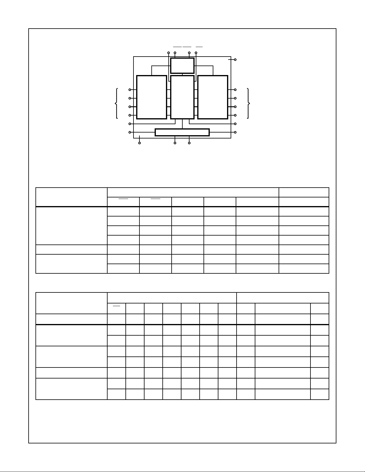
Functional Diagram
CD74HC299, CD74HCT299
CP OE1 OE2 MR
12 2 3 9
THREE-
STATE
CONTROL
20
V
CC
BUS LINE
OUTPUTS
STANDARD
OUTPUT
I/O
I/O
I/O
I/O
Q0
S0
7
0
6
2
5
4
4
6
8
1
I/O
THREE-STATE
OUTPUTS
10 11 18
GND
SHIFT
REGISTER
MODE SELECTION
DS0 DS7
I/O
THREE-STATE
OUTPUTS
13
I/O
14
I/O
15
I/O
16
I/O
17
Q7
19
S1
1
3
BUS LINE
OUTPUTS
5
7
STANDARD
OUTPUT
MODE SELECT FUNCTION TABLE THREE-STATE I/O PORT OPERATING MODE
INPUTS INPUTS/OUTPUTS
FUNCTION
OE1 OE2 S0 S1 Qn (REGISTER) I/O0 --- I/O7
Read Register L L L X L L
L
LL
XH H
LLXL L L
LLXL H H
Load Register X X H H Qn = I/On I/On = Inputs
Disable I/O H X X X X (Z)
X H X X X (Z)
TRUTH TABLE
INPUTS REGISTER OUTPUTS
FUNCTION
MR CP S0 S1 DS0 DS7 I/On Q0 Q1 --- Q6 Q7
RESET (CLEAR) L XXXXXXLL---LL
Shift Right H ↑ hllXXLq
H ↑ hlhXXHq
Shift Left H ↑ lhXlXq
H ↑ lhXhXq
Hold (Do Nothing) H ↑ l l XXXq
q2 --- q
1
q
1
q
0
0
0
2
1
--- q
--- q
--- q
--- q
q
5
5
7
7
6
Q6
H
q
6
L
7
Parallel Load H ↑ hhXXlLL---LL
H↑h h X X h H H --- H H
NOTE: H = Input Voltage High Level, h = Input voltage high one set-up timer prior clock transition; L = Input Voltage Low Level; l = Input
voltage low one set-up time prior clock transition; qn = Lower case letter indicates the state of the reference output one set-up time prior to
clock transition; X - Voltage level on logic status don’t care; Z = Output in high impedance state, ↑ = Low to High Clock Transition.
2
CD74HC299, CD74HCT299
Absolute Maximum Ratings Thermal Information
DC Supply Voltage, VCC. . . . . . . . . . . . . . . . . . . . . . . . -0.5V to 7V
DC Input Diode Current, I
IK
For VI < -0.5V or VI > VCC + 0.5V. . . . . . . . . . . . . . . . . . . . . .±20mA
DC Output Diode Current, I
OK
For VO < -0.5V or VO > VCC + 0.5V . . . . . . . . . . . . . . . . . . . .±20mA
DC Drain Current, per Output, IO,For -0.5V < VO < VCC + 0.5V
For Q Outputs. . . . . . . . . . . . . . . . . . . . . . . . . . . . . . . . . . . . . . .±25mA
For I/O Outputs. . . . . . . . . . . . . . . . . . . . . . . . . . . . . . . . . . . . . .±35mA
DC Output Source or Sink Current per Output Pin, I
O
For VO > -0.5V or VO < VCC + 0.5V . . . . . . . . . . . . . . . . . . . .±25mA
DC VCC or Ground Current, ICC . . . . . . . . . . . . . . . . . . . . . . . . .±50mA
Operating Conditions
Temperature Range, TA . . . . . . . . . . . . . . . . . . . . . . -55oC to 125oC
Supply Voltage Range, V
HC Types . . . . . . . . . . . . . . . . . . . . . . . . . . . . . . . . . . . . .2V to 6V
HCT Types . . . . . . . . . . . . . . . . . . . . . . . . . . . . . . . . .4.5V to 5.5V
DC Input or Output Voltage, VI, VO . . . . . . . . . . . . . . . . . 0V to V
Input Rise and Fall Time
2V . . . . . . . . . . . . . . . . . . . . . . . . . . . . . . . . . . . . . . 1000ns (Max)
4.5V. . . . . . . . . . . . . . . . . . . . . . . . . . . . . . . . . . . . . . 500ns (Max)
6V . . . . . . . . . . . . . . . . . . . . . . . . . . . . . . . . . . . . . . . 400ns (Max)
CAUTION: Stresses above those listed in “Absolute Maximum Ratings” may cause permanent damage to the device. This is a stress only rating and operation
of the device at these or any other conditions above those indicated in the operational sections of this specification is not implied.
NOTE:
3. θJA is measured with the component mounted on an evaluation PC board in free air.
CC
Thermal Resistance (Typical, Note 3) θJA (oC/W)
PDIP Package. . . . . . . . . . . . . . . . . . . . . . . . . . . . . 125
SOIC Package. . . . . . . . . . . . . . . . . . . . . . . . . . . . . 120
Maximum Junction Temperature . . . . . . . . . . . . . . . . . . . . . . . 150oC
Maximum Storage Temperature Range . . . . . . . . . .-65oC to 150oC
Maximum Lead Temperature (Soldering 10s) . . . . . . . . . . . . . 300oC
(SOIC - Lead Tips Only)
CC
DC Electrical Specifications
PARAMETER SYMBOL
HC TYPES
High Level Input
Voltage
Low Level Input
Voltage
High Level Output
Voltage
CMOS Loads
High Level Output
Voltage
TTL Loads
Low Level Output
Voltage
CMOS Loads
Low Level Output
Voltage
TTL Loads
Input Leakage
Current
V
IH
V
IL
V
V
OH
OL
I
VIHor V
VIHor V
VCC or
I
TEST
CONDITIONS
(V) IO(mA) MIN TYP MAX MIN MAX MIN MAX
I
V
CC
(V)
o
C -40oC TO 85oC -55oCTO125oC
25
- - 2 1.5 - - 1.5 - 1.5 - V
4.5 3.15 - - 3.15 - 3.15 - V
6 4.2 - - 4.2 - 4.2 - V
- - 2 - - 0.5 - 0.5 - 0.5 V
4.5 - - 1.35 - 1.35 - 1.35 V
6 - - 1.8 - 1.8 - 1.8 V
-0.02 2 1.9 - - 1.9 - 1.9 - V
IL
4.5 4.4 - - 4.4 - 4.4 - V
6 5.9 - - 5.9 - 5.9 - V
Qn I/On ----- - - - V
-4 -6 4.5 3.98 - - 3.84 - 3.7 - V
-5.2 -7.8 6 5.48 - - 5.34 - 5.2 - V
0.02 2 - - 0.1 - 0.1 - 0.1 V
IL
4.5 - - 0.1 - 0.1 - 0.1 V
6 - - 0.1 - 0.1 - 0.1 V
Qn I/On ----- - - - V
4 6 4.5 - - 0.26 - 0.33 - 0.4 V
5.2 7.8 6 - - 0.26 - 0.33 - 0.4 V
-6--±0.1 - ±1-±1µA
GND
UNITSV
3
 Loading...