


Texas Instruments CD74HCT166M96, CD74HCT166M, CD74HCT166E, CD74HC166M96, CD74HC166M Datasheet
...
Data sheet acquired from Harris Semiconductor SCHS157
February 1998
CD74HC166,
CD74HCT166
High Speed CMOS Logic
8-Bit Parallel-In/Serial-Out Shift Register
|
Features |
|
|
|
at VCC = 5V |
|
|
|
|
||
|
• |
Buffered Inputs |
|
|
• HCT Types |
|
|
|
|
||
|
|
|
- 4.5V to 5.5V Operation |
|
|
|
|||||
|
• |
Typical f |
= 50MHz at V |
= 5V, C |
= 15pF, T = 25oC |
|
|
|
|||
[ /Title |
- Direct LSTTL Input Logic Compatibility, |
|
|
||||||||
|
|
MAX |
CC |
L |
A |
|
|
||||
(CD74 |
• |
Fanout (Over Temperature Range) |
|
VIL= 0.8V (Max), VIH = 2V (Min) |
|
|
|||||
HC166 |
|
- Standard Outputs . . . . . . . . . . . . . . . 10 LSTTL Loads |
- CMOS Input Compatibility, Il ≤ 1 A at VOL, VOH |
||||||||
|
- |
Bus Driver Outputs . . . . . . . . . . . . . 15 LSTTL Loads |
Ordering Information |
|
|
|
|||||
, |
|
|
|
|
|||||||
• Wide Operating Temperature Range . . . -55oC to 125oC |
|
|
|
|
|
||||||
CD74 |
|
TEMP. RANGE |
|
PKG. |
|
||||||
HCT16 |
• Balanced Propagation Delay and Transition Times |
PART NUMBER |
(oC) |
PACKAGE |
NO. |
|
|||||
• Significant Power Reduction Compared to LSTTL |
|
|
|
|
|
||||||
6) |
CD74HC166E |
-55 to 125 |
16 Ld PDIP |
E16.3 |
|
||||||
|
Logic ICs |
|
|
|
|
|
|
|
|
||
/Sub- |
|
|
|
|
CD74HCT166E |
-55 to 125 |
16 Ld PDIP |
E16.3 |
|
||
• HC Types |
|
|
|
|
|||||||
ject |
|
|
|
CD74HC166M |
-55 to 125 |
16 Ld SOIC |
M16.15 |
|
|||
|
- |
2V to 6V Operation |
|
|
|
||||||
(High |
|
|
|
CD74HCT166M |
-55 to 125 |
16 Ld SOIC |
M16.15 |
|
|||
|
- |
High Noise Immunity: NIL = 30%, NIH = 30% of VCC |
|
||||||||
Speed |
|
|
|
|
|
|
|||||
|
|
|
|
|
|
CD54HC166W |
-55 to 125 |
Wafer |
|
|
|
CMOS |
|
|
|
|
|
|
|
|
|
|
|
|
|
|
|
|
|
NOTES: |
|
|
|
|
|
Logic |
|
|
|
|
|
|
1. When ordering, use the entire part number. Add the suffix 96 to |
||||
8-Bit |
|
|
|
|
|
|
obtain the variant in the tape and reel. |
|
|
||
Paral- |
|
|
|
|
|
|
2. Wafer and die is available which meets all electrical |
|
|
||
|
|
|
|
|
|
specifications. Please contact your local sales office or Harris |
|||||
lel- |
|
|
|
|
|
|
|||||
|
|
|
|
|
|
customer service for ordering information. |
|
|
|||
In/Seri |
|
|
|
|
|
|
|
|
|
|
|
|
|
|
|
|
|
|
|
|
|
|
|
|
|
|
|
|
|
|
|
|
|
|
|
|
|
|
|
|
|
|
|
|
|
||
|
Pinout |
|
|
CD74HC166, CD74HCT166 (PDIP, SOIC) |
|
|
|
|
|||
|
|
|
|
|
|
|
|
|
|
||
|
|
|
|
|
|
TOP VIEW |
|
|
|
|
|
DS |
1 |
16 VCC |
D0 |
2 |
15 PE |
D1 |
3 |
14 |
D7 |
D2 |
4 |
13 |
Q7 |
D3 |
5 |
12 |
D6 |
CE |
6 |
11 D5 |
CP |
7 |
10 D4 |
GND |
8 |
9 |
MR |
CAUTION: These devices are sensitive to electrostatic discharge. Users should follow proper IC Handling Procedures. |
File Number 1501.1 |
|
Copyright © Harris Corporation 1998
1
CD74HC166, CD74HCT166
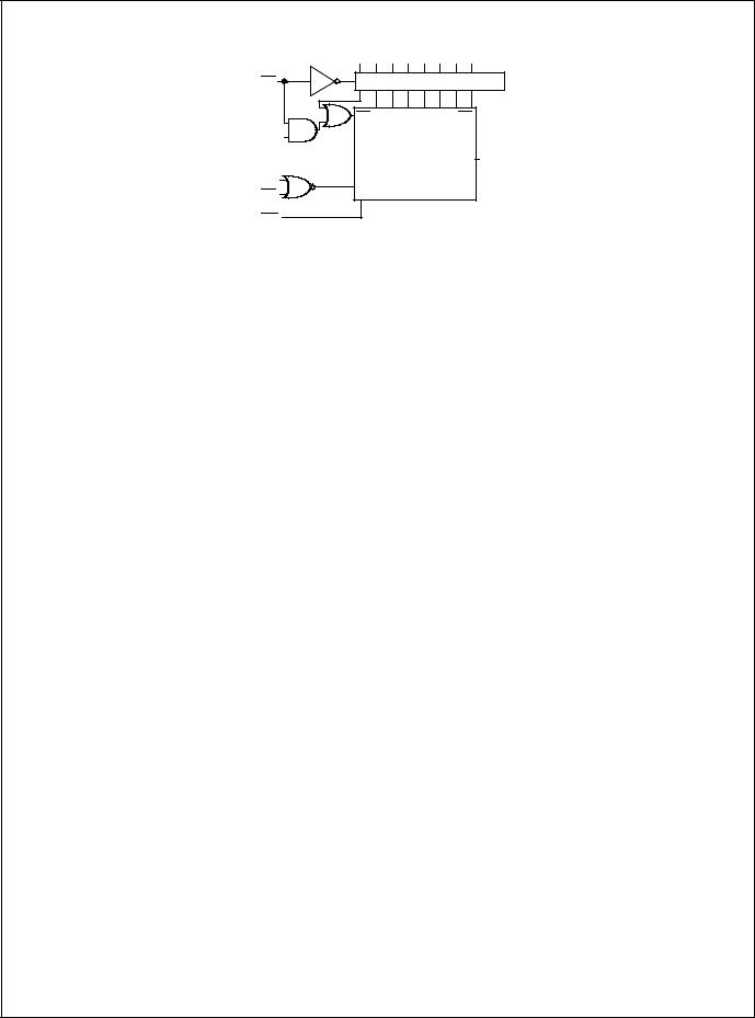
Functional Diagram
|
D0 D1 D2 D3 D4 D5 D6 D7 |
|
PE |
PARALLEL ENABLE CIRCUIT |
|
|
D0 |
D7 |
DS |
|
8 - REGISTERS |
|
|
Q7 |
CP |
|
|
CE |
|
|
MR |
|
|
TRUTH TABLE
|
|
INPUTS |
|
|
INTERNAL |
|
||
|
|
|
|
|
|
|
||
MASTER |
PARALLEL |
CLOCK |
|
|
PARALLEL |
Q STATES |
OUTPUT |
|
|
|
|
|
|
||||
RESET |
ENABLE |
ENABLE |
CLOCK |
SERIAL |
D0 D7 |
Q0 |
Q1 |
Q7 |
|
|
|
|
|
|
|
|
|
L |
X |
X |
X |
X |
X |
L |
L |
L |
|
|
|
|
|
|
|
|
|
H |
X |
L |
L |
X |
X |
Q00 |
Q10 |
Q0 |
|
|
|
|
|
|
|
|
|
H |
L |
L |
↑ |
X |
a...h |
a |
b |
h |
|
|
|
|
|
|
|
|
|
H |
H |
L |
↑ |
H |
X |
H |
Q0n |
Q6n |
|
|
|
|
|
|
|
|
|
H |
H |
L |
↑ |
L |
X |
L |
Q0n |
Q6n |
|
|
|
|
|
|
|
|
|
H |
X |
H |
↑ |
X |
X |
Q00 |
Q10 |
Q70 |
|
|
|
|
|
|
|
|
|
NOTES:
H = High Voltage Level
L = Low Voltage Level X = Don’t Care
↑ = Transition from Low to High Level
a...h = The level of steady-state input at inputs D0 thru D7, respectively.
Q00, Q10, Q70 = The level of Q0, Q1, or Q7, respectively, before the indicated steady-state input conditions were established. Q0n, Q6n = The level of Q0 or Q6, respectively, before the most recent ↑ transition of the clock.
2

CD74HC166, CD74HCT166
Absolute Maximum Ratings
DC Supply Voltage, VCC . . . . . . . . . . . . . . . . . . . . . . . . |
-0.5V to 7V |
DC Input Diode Current, IIK |
±20mA |
For VI < -0.5V or VI > VCC + 0.5V . . . . . . . . . . . . . . . . . . |
|
DC Output Diode Current, IOK |
±20mA |
For VO < -0.5V or VO > VCC + 0.5V . . . . . . . . . . . . . . . . |
|
DC Drain Current, per Output, IO |
±25mA |
For -0.5V < VO < VCC + 0.5V. . . . . . . . . . . . . . . . . . . . . . |
|
DC Output Source or Sink Current per Output Pin, IO |
±25mA |
For VO > -0.5V or VO < VCC + 0.5V . . . . . . . . . . . . . . . . |
|
DC VCC or Ground Current, ICC or IGND . . . . . . . . . . . . . . |
. . . .±50mA |
Thermal Information |
|
Thermal Resistance (Typical, Note 3) |
θJA (oC/W) |
PDIP Package . . . . . . . . . . . . . . . . . . . . . . . . . . . . |
. 90 |
SOIC Package . . . . . . . . . . . . . . . . . . . . . . . . . . . . |
. 160 |
Maximum Junction Temperature . . . . . . . . . . . . . . . . |
. . . . . . . 150oC |
Maximum Storage Temperature Range . . . . . . . . . . |
-65oC to 150oC |
Maximum Lead Temperature (Soldering 10s) . . . . . . |
. . . . . . . 300oC |
(SOIC - Lead Tips Only) |
|
Operating Conditions
Temperature Range (TA) . . . . . . . . . . . . . . . . . . . . . -55oC to 125oC Supply Voltage Range, VCC
HC Types . . . . . . . . . . . . . . . . . . . . . . . . . . . . . . . . . . . . .2V to 6V HCT Types . . . . . . . . . . . . . . . . . . . . . . . . . . . . . . . . .4.5V to 5.5V
DC Input or Output Voltage, VI, VO . . . . . . . . . . . . . . . . . 0V to VCC Input Rise and Fall Time
2V . . . . . . . . . . . . . . . . . . . . . . . . . . . . . . . . . . . . . . 1000ns (Max) 4.5V. . . . . . . . . . . . . . . . . . . . . . . . . . . . . . . . . . . . . . 500ns (Max)
6V . . . . . . . . . . . . . . . . . . . . . . . . . . . . . . . . . . . . . . . 400ns (Max)
CAUTION: Stresses above those listed in “Absolute Maximum Ratings” may cause permanent damage to the device. This is a stress only rating and operation of the device at these or any other conditions above those indicated in the operational sections of this specification is not implied.
NOTE:
3. θJA is measured with the component mounted on an evaluation PC board in free air.
DC Electrical Specifications
|
|
TEST |
|
|
25oC |
|
-40oC TO 85oC |
-55oC TO 125oC |
|
|||
|
|
CONDITIONS |
|
|
|
|
||||||
PARAMETER |
SYMBOL |
VI (V) |
IO (mA) |
VCC (V) |
MIN |
TYP |
MAX |
MIN |
MAX |
MIN |
MAX |
UNITS |
HC TYPES |
|
|
|
|
|
|
|
|
|
|
|
|
|
|
|
|
|
|
|
|
|
|
|
|
|
High Level Input |
VIH |
- |
- |
2 |
1.5 |
- |
- |
1.5 |
- |
1.5 |
- |
V |
Voltage |
|
|
|
|
|
|
|
|
|
|
|
|
|
|
|
4.5 |
3.15 |
- |
- |
3.15 |
- |
3.15 |
- |
V |
|
|
|
|
|
|||||||||
|
|
|
|
|
|
|
|
|
|
|
|
|
|
|
|
|
6 |
4.2 |
- |
- |
4.2 |
- |
4.2 |
- |
V |
|
|
|
|
|
|
|
|
|
|
|
|
|
Low Level Input |
VIL |
- |
- |
2 |
- |
- |
0.5 |
- |
0.5 |
- |
0.5 |
V |
Voltage |
|
|
|
|
|
|
|
|
|
|
|
|
|
|
|
4.5 |
- |
- |
1.35 |
- |
1.35 |
- |
1.35 |
V |
|
|
|
|
|
|||||||||
|
|
|
|
|
|
|
|
|
|
|
|
|
|
|
|
|
6 |
- |
- |
1.8 |
- |
1.8 |
- |
1.8 |
V |
|
|
|
|
|
|
|
|
|
|
|
|
|
High Level Output |
VOH |
VIH or |
-0.02 |
2 |
1.9 |
- |
- |
1.9 |
- |
1.9 |
- |
V |
Voltage |
|
VIL |
|
|
|
|
|
|
|
|
|
|
|
-0.02 |
4.5 |
4.4 |
- |
- |
4.4 |
- |
4.4 |
- |
V |
||
CMOS Loads |
|
|
||||||||||
|
|
|
|
|
|
|
|
|
|
|
|
|
|
|
|
-0.02 |
6 |
5.9 |
- |
- |
5.9 |
- |
5.9 |
- |
V |
|
|
|
|
|
|
|
|
|
|
|
|
|
High Level Output |
|
|
-4 |
4.5 |
3.98 |
- |
- |
3.84 |
- |
3.7 |
- |
V |
Voltage |
|
|
|
|
|
|
|
|
|
|
|
|
|
|
-5.2 |
6 |
5.48 |
- |
- |
5.34 |
- |
5.2 |
- |
V |
|
TTL Loads |
|
|
||||||||||
|
|
|
|
|
|
|
|
|
|
|
|
|
|
|
|
|
|
|
|
|
|
|
|
|
|
Low Level Output |
VOL |
VIH or |
0.02 |
2 |
- |
- |
0.1 |
- |
0.1 |
- |
0.1 |
V |
Voltage |
|
VIL |
|
|
|
|
|
|
|
|
|
|
|
0.02 |
4.5 |
- |
- |
0.1 |
- |
0.1 |
- |
0.1 |
V |
||
CMOS Loads |
|
|
||||||||||
|
|
|
|
|
|
|
|
|
|
|
|
|
|
|
|
0.02 |
6 |
- |
- |
0.1 |
- |
0.1 |
- |
0.1 |
V |
|
|
|
|
|
|
|
|
|
|
|
|
|
Low Level Output |
|
|
4 |
4.5 |
- |
- |
0.26 |
- |
0.33 |
- |
0.4 |
V |
Voltage |
|
|
|
|
|
|
|
|
|
|
|
|
|
|
5.2 |
6 |
- |
- |
0.26 |
- |
0.33 |
- |
0.4 |
V |
|
TTL Loads |
|
|
||||||||||
|
|
|
|
|
|
|
|
|
|
|
|
|
|
|
|
|
|
|
|
|
|
|
|
|
|
Input Leakage |
II |
VCC or |
- |
6 |
- |
- |
±0.1 |
- |
±1 |
- |
±1 |
µA |
Current |
|
GND |
|
|
|
|
|
|
|
|
|
|
|
|
|
|
|
|
|
|
|
|
|
|
|
3
 Loading...