


CD74HCT165M96
Texas Instruments CD74HCT165M96, CD74HCT165M, CD74HCT165E, CD74HC165M96, CD74HC165M Datasheet
...
CD74HC165,
/
[ /Title
(CD74H
C165,
CD74H
CT165)
Subject
(High
Speed
CMOS
Logic 8Bit Parallel-
Data sheet acquired from Harris Semiconductor
SCHS156
February 1998
Features
• Buffered Inputs
• Asynchronous Parallel Load
• Complementary Outputs
• Typical f
T
= 25oC
A
• Fanout (Over Temperature Range)
- Standard Outputs. . . . . . . . . . . . . . . 10 LSTTL Loads
- Bus Driver Outputs . . . . . . . . . . . . . 15 LSTTL Loads
• Wide Operating Temperature Range . . . -55
• Balanced Propagation Delay and Transition Times
• Significant Power Reduction Compared to LSTTL
Logic ICs
• HC Types
- 2V to 6V Operation
- High Noise Immunity: N
at VCC = 5V
• HCT Types
- 4.5V to 5.5V Operation
- Direct LSTTL Input Logic Compatibility,
V
= 0.8V (Max), VIH = 2V (Min)
IL
- CMOS Input Compatibility, I
= 60MHz at VCC = 5V, CL = 15pF,
MAX
= 30%, NIH = 30% of V
IL
≤ 1µA at VOL, V
l
o
CD74HCT165
High Speed CMOS Logic
8-Bit Parallel-In/Serial-Out Shift Register
C to 125oC
CC
OH
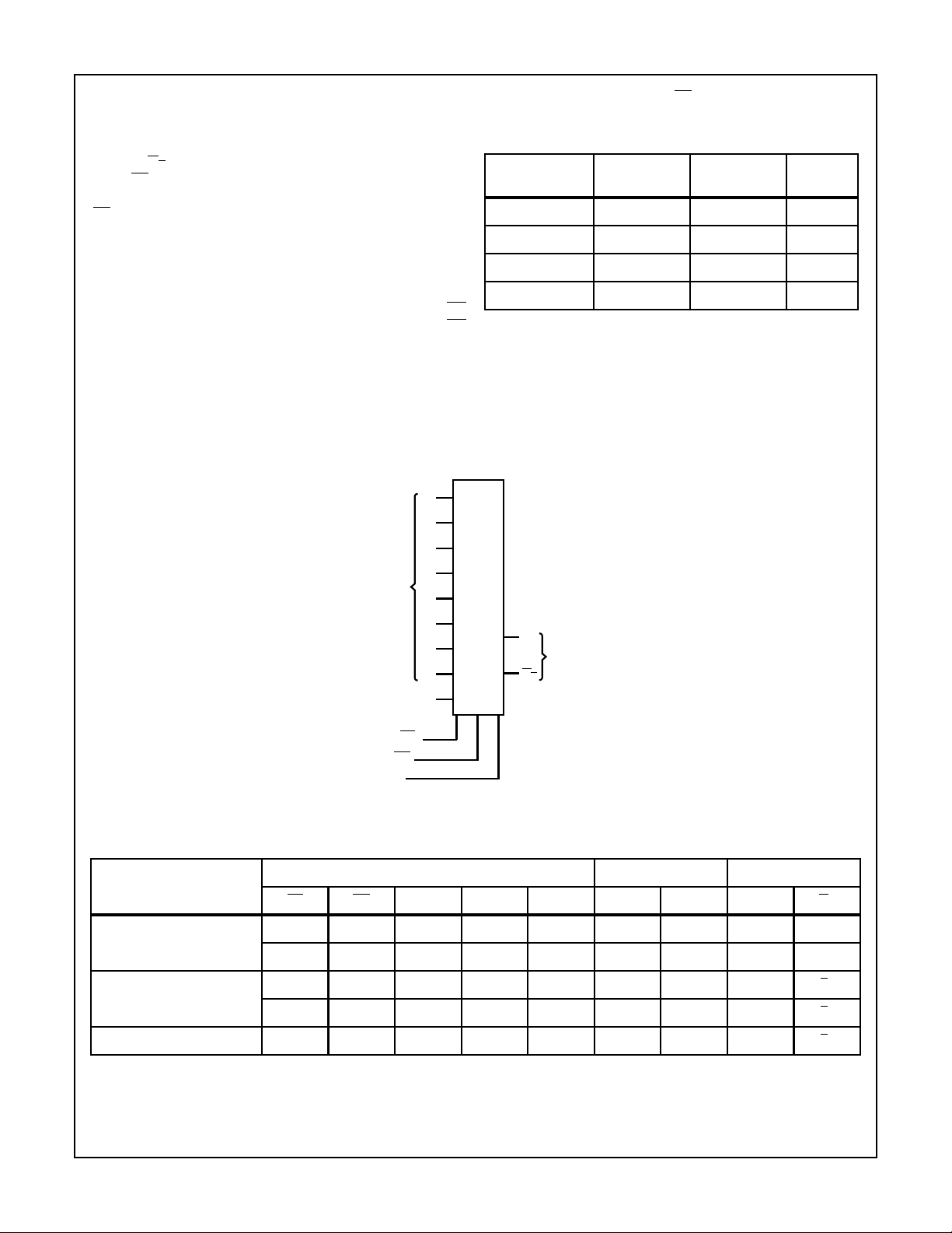
Pinout
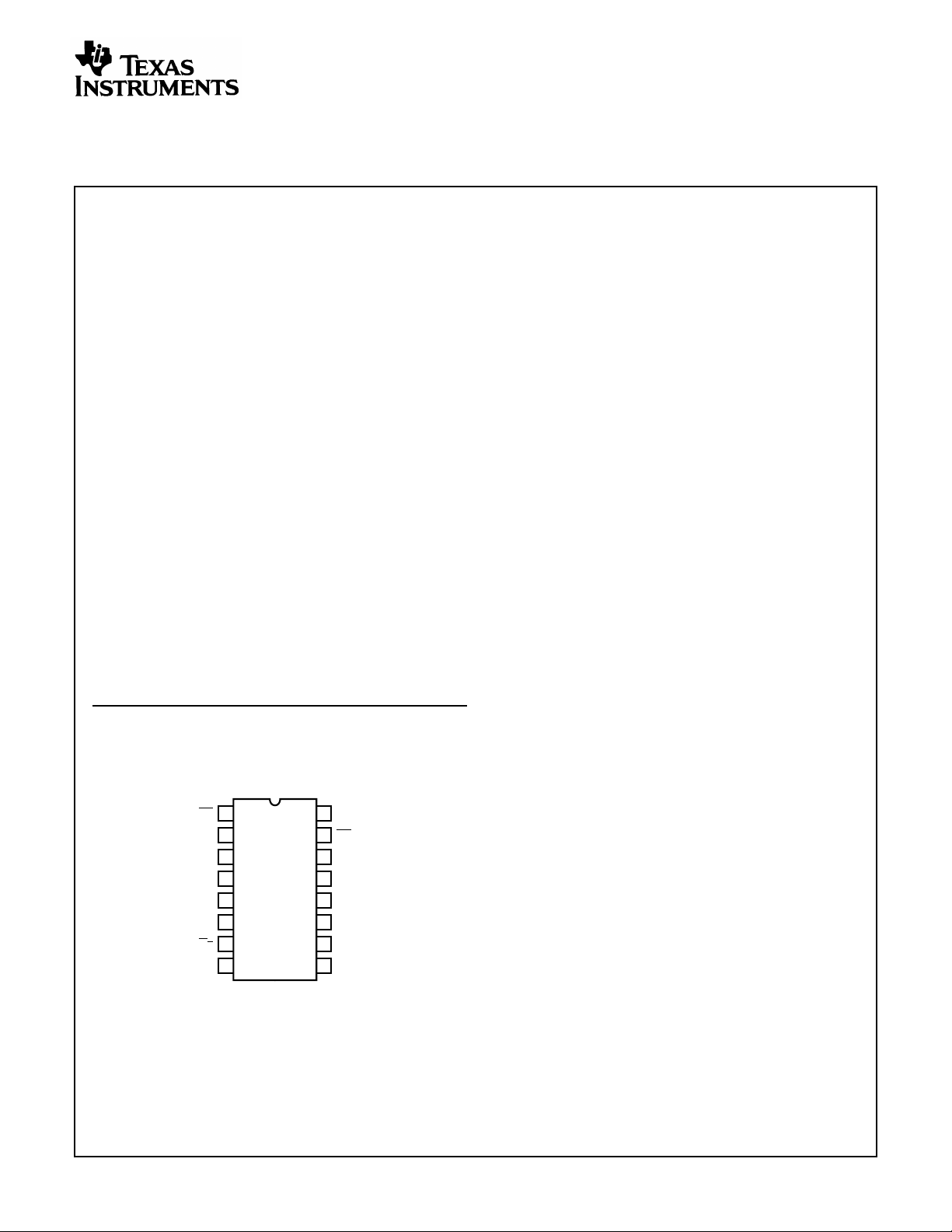
CD74HC165, CD74HCT165
(PDIP, SOIC)
TOP VIEW
16
1
PL
2
CP
3
D4
4
D5
5
D6
6
D7
7
Q
7
8
GND
CAUTION: These devices are sensitive to electrostatic discharge. Users should follow proper IC Handling Procedures.
Copyright
© Harris Corporation 1998
V
CC
15
CE
14
D3
13
D2
12
D1
D0
11
10
DS
9
Q
7
1
File Number 1672.1
CD74HC165, CD74HCT165
Description
The Harris CD74HC165 and CD74HCT165 are 8-bit parallel
or serial-in shift registers with complementary serial outputs
(Q
and Q7) available from the last stage. When the parallel
7
load (
PL) input is LOW, parallel data from the D0 to D7
inputs are loaded into the register asynchronously. When the
PL is HIGH, data enters the register serially at the DS input
and shifts one place to the right (Q
0→Q1→Q2
, etc.) with
each positive-going clock transition. This feature allow parallel-to-serial converter expansion by typing the Q
output to
7
the DS input of the succeeding device.
For predictable operation the LOW-to-HIGH transition of
should only take place while CP is HIGH. Also, CP an d
CE
CE
should be LOW before the LOW-to-HIGH transition of PL to
Functional Diagram
11
D0
12
D1
13
D2
PARALLEL
DAT A
INPUTS
D3
D4
D5
D6
D7
DS
14
3
4
5
6
10
prevent shifting the data when
PL goes HIGH.
Ordering Information
TEMP.RANGE
PART NUMBER
CD74HC165E -55 to 125 16 Ld PDIP E16.3
CD74HCT165E -55 to 125 16 Ld PDIP E16.3
CD74HC165M -55 to 125 16 Ld SOIC M16.15
CD74HCT165M -55 to 125 16 Ld SOIC M16.15
NOTES:
1. When ordering, use the entire partnumber. Add the suffix 96 to
obtain the variant in the tape and reel.
2. Wafer and die is available which meets all electrical
specifications. Please contact your local sales office or Harris
customer service for ordering information.
9
Q
7
SERIAL
7
OUTPUTS
Q
7
(oC) PACKAGE PKG. NO.
151
PL
CE
CP
2
GND = 8
VCC = 16
TRUTH TABLE
INPUTS Qn REGISTER OUTPUTS
OPERATING MODE
PL CE CP DS D0 - D7 Q
Q1 - Q
0
Q
6
7
Parallel Load L X X X L L L-L L H
LXXXHHH-HHL
Serial Shift H L ↑ lXLq
HL↑ hXHq
Hold Do Nothing H H X X X q
0
0 -q5
0 -q5
q
1 -q6
q
6
q
6
q
7
Q
7
q
6
q
6
q
7
2
CD74HC165, CD74HCT165
TRUTH TABLE
INPUTS Qn REGISTER OUTPUTS
OPERATING MODE
NOTE:
H = High Voltage Level
h = High Voltage Level One Set-up Time Prior To The Low-to-high Clock Transition
l = Low Voltage Level One Set-up Time Prior To The Low-to-high Clock Transition
L = Low Voltage Level
X = Don’t Care
↑ = Transition from Low to High Level
qn= Lower Case Letters Indicate The State Of the Reference Output Clock Transition
PL CE CP DS D0 - D7 Q
Q1 - Q
0
Q
6
7
Q
7
3
 Loading...