


Texas Instruments CD74FCT573SM96, CD74FCT573SM, CD74FCT573M96, CD74FCT573M, CD74FCT573E Datasheet
...
CD74FCT573AT was not acquired from Harris Semiconductor.
|
|
|
|
|
|
CD74FCT573, |
||||||||||
Data sheet acquired from Harris Semiconductor |
|
|
CD74FCT573AT |
|||||||||||||
SCHS260A |
|
|
|
|
|
BiCMOS FCT Interface Logic, |
||||||||||
|
|
|
|
|
|
|||||||||||
January 1997 |
|
RECOMMENDED |
Octal Transparent Latches, Three-State |
|||||||||||||
|
NOT |
|
|
|
|
|
|
|
|
|
|
|
|
|||
Features |
|
NEW |
DESIGNS |
|
Description |
|
|
|
|
|
|
|
|
|
||
FOR |
Technology |
|
|
|
|
|
|
|
|
|
|
|||||
CMOS |
|
|
|
|
|
|
|
|
|
|
||||||
• Buffered Inputs |
Use |
|
|
The CD74FCT573 and CD74FCT573AT octal transparent |
||||||||||||
|
|
|
||||||||||||||
|
|
|
|
|
||||||||||||
• Typical Propagation Delay: 3.9ns at VCC = 5V, |
|
latches use a small geometry BiCMOS technology. The out- |
||||||||||||||
TA = 25oC, CL = 50pF (CD74FCT573AT) |
|
put stage is a combination of bipolar and CMOS transistors |
||||||||||||||
• SCR Latchup Resistant BiCMOS Process and |
|
that limits the output HIGH level to two diode drops below |
||||||||||||||
|
VCC. This resultant lowering of output swing (0V to 3.7V) |
|||||||||||||||
Circuit Design |
|
|
|
|
|
|||||||||||
• FCTXXX Types |
|
|
|
|
|
reduces power bus ringing (a source of EMI) and minimizes |
||||||||||
|
|
|
|
|
VCC bounce and ground bounce and their effects during |
|||||||||||
- Speed of Bipolar FAST™/AS/S |
|
|
||||||||||||||
|
|
simultaneous output switching. The output configuration |
||||||||||||||
|
|
|
|
|
|
|||||||||||
• FCTXXXAT Types |
|
|
|
|
|
also enhances switching speed and is capable of sinking |
||||||||||
|
|
|
|
|
48 milliamperes. |
|
|
|
|
|
|
|
|
|
||
- 30% Faster than FAST™/AS/S with Significantly |
|
|
|
|
|
|
|
|
|
|
||||||
|
|
|
|
|
|
|
|
|
|
|
|
|||||
Reduced Power Consumption |
|
|
The CD74FCT573 and CD74FCT573AT outputs are trans- |
|||||||||||||
• 48mA Output Sink Current |
|
|
|
parent to the inputs when the Latch Enable |
(LE) |
is HIGH. |
||||||||||
|
|
|
|
|
|
|
|
|
|
|
|
|
|
|||
|
|
|
When the Latch Enable (LE) goes LOW, the data is latched. |
|||||||||||||
• Output Voltage Swing Limited to 3.7V at VCC = 5V |
|
|||||||||||||||
|
The Output Enable |
(OE) |
controls the three-state outputs. |
|||||||||||||
• Controlled Output Edge Rates |
|
|
When the Output Enable |
|
is HIGH, the outputs are in |
|||||||||||
|
(OE) |
|||||||||||||||
• Input/Output Isolation to VCC |
|
|
the high impedance state. The latch operation is indepen- |
|||||||||||||
• BiCMOS Technology with Low Quiescent Power |
|
dent of the state of the Output Enable. |
|
|
||||||||||||
|
|
|
|
|
|
Ordering Information |
|
|
|
|
|
|||||
|
|
|
|
|
|
|
|
|
|
|
|
|
|
|||
|
|
|
|
|
|
|
|
TEMP. |
|
|
|
PKG. |
|
|||
|
|
|
|
|
|
PART NUMBER |
|
RANGE (oC) |
PACKAGE |
|
NO. |
|
||||
|
|
|
|
|
|
CD74FCT573ATE |
|
0 to 70 |
20 Ld PDIP |
|
E20.3 |
|
||||
|
|
|
|
|
|
|
|
|
|
|
|
|
||||
|
|
|
|
|
|
CD74FCT573M |
|
0 to 70 |
20 Ld SOIC |
|
M20.3 |
|
||||
|
|
|
|
|
|
|
|
|
|
|
|
|
||||
|
|
|
|
|
|
CD74FCT573SM |
|
0 to 70 |
20 Ld SSOP |
|
M20.209 |
|
||||
|
|
|
|
|
|
|
|
|
|
|
||||||
|
|
|
|
|
|
NOTE: When ordering the suffix M and SM packages, use the entire |
||||||||||
|
|
|
|
|
|
part number. Add the suffix 96 to obtain the variant in the tape and reel. |
||||||||||
Pinout
CD74FCT573, CD74FCT573AT
|
(PDIP, SOIC, SSOP) |
|
|
|
|
TOP VIEW |
|
OE |
1 |
20 |
VCC |
D0 |
2 |
19 |
Q0 |
D1 |
3 |
18 |
Q1 |
D2 |
4 |
17 |
Q2 |
D3 |
5 |
16 |
Q3 |
D4 |
6 |
15 |
Q4 |
D5 |
7 |
14 |
Q5 |
D6 |
8 |
13 |
Q6 |
D7 |
9 |
12 |
Q7 |
GND |
10 |
11 LE |
CAUTION: These devices are sensitive to electrostatic discharge. Users should follow proper IC Handling Procedures. |
File Number 2304.2 |
|
|
||
FAST™ is a trademark of Fairchild Semiconductor. |
8-1 |
|
Copyright © Harris Corporation 1997 |
|
|
|
|
|
CD74FCT573, CD74FCT573AT
Functional Diagram
|
D0 |
2 |
|
|
|
19 |
Q0 |
||
|
3 |
|
|
|
18 |
||||
|
D1 |
|
|
|
Q1 |
||||
|
4 |
|
|
|
17 |
||||
|
D2 |
|
|
|
Q2 |
||||
|
5 |
|
|
|
16 |
||||
|
D3 |
|
|
|
Q3 |
||||
|
6 |
|
|
|
15 |
||||
|
D4 |
|
|
|
Q4 |
||||
|
7 |
|
|
|
14 |
||||
|
D5 |
|
|
|
Q5 |
||||
|
8 |
|
|
|
13 |
||||
|
D6 |
|
|
|
Q6 |
||||
|
9 |
|
|
|
12 |
||||
|
D7 |
|
|
|
Q7 |
||||
|
|
|
|
|
|
||||
|
|
|
|
|
|
|
|
|
|
|
|
|
|
11 |
1 |
|
|
|
|
|
LE |
|
|
GND = PIN 10 |
|||||
|
|
|
|
|
|
||||
|
|
|
|
|
|
|
|
||
OE |
|
|
|
|
|
|
VCC = PIN 20 |
||
|
|
|
|
|
|||||
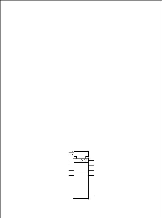
TRUTH TABLE (Note 1)
|
|
|
|
|
|
|
|
|
OUTPUT |
|
LATCH |
|
|
||
|
ENABLE |
|
ENABLE |
DATA |
OUTPUT |
||
|
|
|
|
|
|
|
|
|
L |
|
|
H |
H |
H |
|
|
|
|
|
|
|
|
|
|
L |
|
|
H |
L |
L |
|
|
|
|
|
|
|
|
|
|
L |
|
|
L |
l |
L |
|
|
|
|
|
|
|
|
|
|
L |
|
|
L |
h |
H |
|
|
|
|
|
|
|
|
|
|
H |
|
|
X |
X |
Z |
|
|
|
|
|
|
|
|
|
NOTE:
1.H = HIGH Voltage Level L = LOW Voltage Level
l = Low voltage level one set up time prior to the high to low latch enable transition. h = High voltage level one set up time prior to the high to low latch enable transition. X = Irrelevant
Z = High Impedance
IEC Logic Symbol
CD74FCT573, CD74FCT573AT
1 |
EN |
|
11 |
|
|
C1 |
|
|
2 |
1D |
19 |
|
|
3 |
|
18 |
4 |
|
17 |
5 |
|
16 |
6 |
|
15 |
|
||
7 |
|
14 |
|
||
8 |
|
13 |
|
||
9 |
|
12 |
|
||
|
|
|
8-2

CD74FCT573, CD74FCT573AT
Absolute Maximum Ratings
DC Supply Voltage (VCC) . . . . . . . . . . . . . . . . . . . . . . . . -0.5V to 6V DC Input Diode Current, IIK (For VI < -0.5V) . . . . . . . . . . . . . -20mA DC Output Diode Current, IOK (for VO < -0.5V) . . . . . . . . . . . -50mA
DC Output Sink Current per Output Pin, IO . . . . . . . . . . . . . . . 70mA DC Output Source Current per Output Pin, IO . . . . . . . . . . . . -30mA
DC VCC Current (ICC) . . . . . . . . . . . . . . . . . . . . . . . . . . . . . . 140mA DC Ground Current (IGND). . . . . . . . . . . . . . . . . . . . . . . . . . . 400mA
Thermal Information |
|
Thermal Resistance (Typical, Note 2) |
θJA (oC/W) |
PDIP Package . . . . . . . . . . . . . . . . . . . . . . . . . . . . |
. . . . . 135 |
SOIC Package . . . . . . . . . . . . . . . . . . . . . . . . . . . . |
. . . . . 125 |
SSOP Package . . . . . . . . . . . . . . . . . . . . . . . . . . . |
. . . . . 130 |
Maximum Junction Temperature . . . . . . . . . . . . . . . . |
. . . . . . . 150oC |
Maximum Storage Temperature Range . . . . . . . . . . |
-65oC to 150oC |
Maximum Lead Temperature (Soldering 10s) . . . . . . |
. . . . . . . 300oC |
(SOIC and SSOP-Lead Tips Only) |
|
Operating Conditions
Operating Temperature Range (TA) . . . . . . . . . . . . . . . .0oC to 70oC
Supply Voltage Range, VCC . . . . . . . . . . . . . . . . . . . .4.75V to 5.25V
DC Input Voltage, VI . . . . . . . . . . . . . . . . . . . . . . . . . . . . . . 0 to VCC
DC Output Voltage, VO . . . . . . . . . . . . . . . . . . . . . . . . . . . 0 to ≤ VCC
Input Rise and Fall Slew Rate, dt/dv. . . . . . . . . . . . . . . . 0 to 10ns/V
CAUTION: Stresses above those listed in “Absolute Maximum Ratings” may cause permanent damage to the device. This is a stress only rating and operation of the device at these or any other conditions above those indicated in the operational sections of this specification is not implied.
NOTE:
2. θJA is measured with the component mounted on an evaluation PC board in free air.
Electrical Specifications |
Commercial Temperature Range 0oC to 70oC, V |
CC |
Max = 5.25V, V |
CC |
Min = 4.75V (Note 5) |
|
||||||||
|
|
|
|
|
|
|
|
|
|
|
|
|
||
|
|
|
|
|
|
|
|
|
|
|
|
|
||
|
|
|
|
|
|
|
|
AMBIENT TEMPERATURE (TA) |
|
|||||
|
|
|
TEST CONDITIONS |
|
|
|
25oC |
|
0oC TO 70oC |
|
||||
PARAMETER |
|
SYMBOL |
VI (V) |
IO (mA) |
VCC (V) |
|
MIN |
|
MAX |
MIN |
MAX |
UNITS |
||
High Level Input Voltage |
|
VIH |
|
|
4.75 to 5.25 |
2 |
|
- |
|
2 |
- |
V |
||
Low Level Input Voltage |
|
VIL |
|
|
4.75 to 5.25 |
- |
|
0.8 |
- |
0.8 |
V |
|||
High Level Output Voltage |
|
VOH |
VIH or VIL |
-15 |
Min |
|
2.4 |
|
- |
|
2.4 |
- |
V |
|
Low Level Output Voltage |
|
VOL |
VIH or VIL |
48 |
Min |
|
- |
|
0.55 |
- |
0.55 |
V |
||
High Level Input Current |
|
IIH |
VCC |
|
Max |
|
- |
|
0.1 |
- |
1 |
μA |
||
Low Level Input Current |
|
IIL |
GND |
|
Max |
|
- |
|
-0.1 |
- |
-1 |
μA |
||
Three-State Leakage Current |
|
IOZH |
VCC |
|
Max |
|
- |
|
0.5 |
- |
10 |
μA |
||
|
|
IOZL |
GND |
|
Max |
|
- |
|
-0.5 |
- |
-10 |
μA |
||
Input Clamp Voltage |
|
VIK |
VCC or |
-18 |
Min |
|
- |
|
-1.2 |
- |
-1.2 |
V |
||
|
|
|
GND |
|
|
|
|
|
|
|
|
|
|
|
|
|
|
|
|
|
|
|
|
|
|
|
|
|
|
Short Circuit Output Current |
|
IOS |
VO = 0 |
|
Max |
|
-60 |
|
- |
|
-60 |
- |
mA |
|
(Note 3) |
|
|
VCC or |
|
|
|
|
|
|
|
|
|
|
|
|
|
|
GND |
|
|
|
|
|
|
|
|
|
|
|
|
|
|
|
|
|
|
|
|
|
|
|
|
|
|
Quiescent Supply Current, |
|
ICC |
VCC or |
0 |
Max |
|
- |
|
8 |
|
- |
80 |
μA |
|
MSI |
|
|
GND |
|
|
|
|
|
|
|
|
|
|
|
|
|
|
|
|
|
|
|
|
|
|
|
|
||
Additional Quiescent Supply |
|
ICC |
3.4V |
|
Max |
|
- |
|
1.6 |
- |
1.6 |
mA |
||
Current per Input Pin |
|
|
(Note 4) |
|
|
|
|
|
|
|
|
|
|
|
TTL Inputs High, 1 Unit Load |
|
|
|
|
|
|
|
|
|
|
|
|
|
|
|
|
|
|
|
|
|
|
|
|
|
|
|
|
|
NOTES: |
|
|
|
|
|
|
|
|
|
|
|
|
|
|
3.Not more than one output should be shorted at one time. Test duration should not exceed 100ms.
4.Inputs that are not measured are at VCC or GND.
5. FCT Input Loading: All inputs are 1 unit load. Unit load is ICC limit specified in Electrical Specifications table, e.g., 1.6mA Max. at 70oC.
8-3
 Loading...