


Texas Instruments CD74HCT14M96, CD74HCT14M, CD74HCT14E, CD74HC14M96, CD74HC14M Datasheet
...Data sheet acquired from Harris Semiconductor SCHS129
January 1998
CD74HC14,
CD74HCT14
High Speed CMOS Logic
Hex Inverting Schmitt Trigger
[ /Title (CD74H C14, CD74H CT14) /Subject (High Speed CMOS Logic Hex Invert-
Features
•Unlimited Input Rise and Fall Times
•Exceptionally High Noise Immunity
•Fanout (Over Temperature Range)
-Standard Outputs . . . . . . . . . . . . . . . 10 LSTTL Loads
-Bus Driver Outputs . . . . . . . . . . . . . 15 LSTTL Loads
•Wide Operating Temperature Range . . . -55oC to 125oC
•Balanced Propagation Delay and Transition Times
•Significant Power Reduction Compared to LSTTL Logic ICs
•HC Types
-2V to 6V Operation
-High Noise Immunity: NIL = 30%, NIH = 30% of VCC
at VCC = 5V
•HCT Types
-4.5V to 5.5V Operation
-Direct LSTTL Input Logic Compatibility, VIL= 0.8V (Max), VIH = 2V (Min)
-CMOS Input Compatibility, Il ≤ 1 A at VOL, VOH
Description
The Harris CD74HC14, CD74HCT14 each contain 6 inverting Schmitt Triggers in one package.
Ordering Information
|
TEMP. RANGE |
|
PKG. |
PART NUMBER |
(oC) |
PACKAGE |
NO. |
CD54HCT14F |
-55 to 125 |
14 Ld CERDIP |
F14.3 |
|
|
|
|
Pinout
CD54HC14, CD54HCT14, CD74HC14, CD74HCT14
(PDIP, CERDIP, SOIC)
TOP VIEW
1A |
1 |
|
14 |
VCC |
1Y |
|
|
|
6A |
2 |
|
13 |
||
2A |
|
|
|
6Y |
3 |
|
12 |
||
2Y |
|
|
|
5A |
4 |
|
11 |
||
3A |
|
|
|
5Y |
5 |
|
10 |
||
3Y |
|
|
|
4A |
6 |
|
9 |
||
GND |
|
|
|
4Y |
7 |
|
8 |
CAUTION: These devices are sensitive to electrostatic discharge. Users should follow proper IC Handling Procedures. |
File Number 1781.1 |
|
|
||
Copyright © Harris Corporation 1998 |
1 |
|
|
|
|

CD74HC14, CD74HCT14
Functional Diagram
1 |
2 |
1A |
1Y |
3 |
4 |
2A |
2Y |
5 |
6 |
3A |
3Y |
9 |
8 |
4A |
4Y |
11 |
10 |
5A |
5Y |
13 |
12 |
6A |
6Y |
|
GND = 7 |
|
VCC = 14 |
|
TRUTH TABLE |
|
|
|
|
INPUT (A) |
|
OUTPUT (Y) |
|
|
|
L |
|
H |
|
|
|
H |
|
L |
|
|
|
NOTE: |
|
|
H= High Level |
|
|
L = Low Level |
|
|
Logic Diagram
nA |
nY |
2
CD74HC14, CD74HCT14
V |
VH |
O |
|
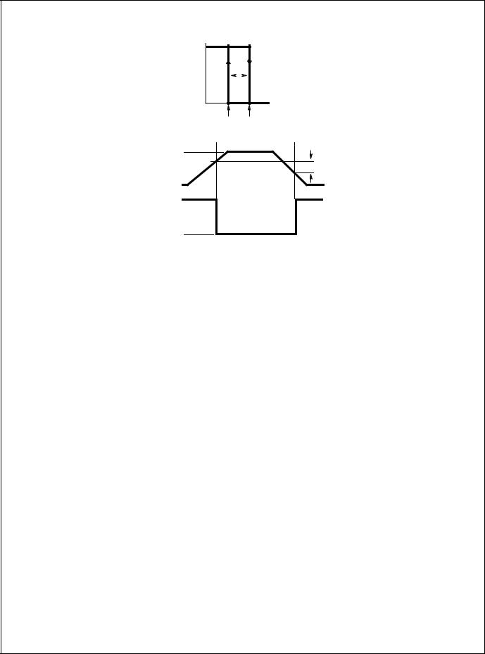
VH = VT+ - VT-
VI
VT- VT+
VT+ |
VT- |
VCC
VI VH
GND
VCC
VO
GND
FIGURE 3. HYSTERESIS DEFINITION, CHARACTERISTIC, AND TEST SETUP
3
 Loading...