Texas Instruments CD74HCT10M96, CD74HCT10M, CD74HCT10E, CD74HC10M96, CD74HC10M Datasheet
...
[ /Title (CD74 HC10, CD74 HCT10
)
/Subject (High Speed CMOS Logic Triple 3-Input NAND Gate) /Autho r () /Keywords (High Speed CMOS Logic Triple 3-Input NAND Gate, High Speed CMOS Logic Triple 3-Input NAND Gate, Harris Semi-
|
CD74HC10, |
Data sheet acquired from Harris Semiconductor |
CD74HCT10 |
SCHS128 |
|
|
High Speed CMOS Logic |
August 1997 |
Triple 3-Input NAND Gate |
Features
•Buffered Inputs
•Typical Propagation Delay: 8ns at VCC = 5V, CL = 15pF, TA = 25oC
•Fanout (Over Temperature Range)
-Standard Outputs . . . . . . . . . . . . . . . 10 LSTTL Loads
-Bus Driver Outputs . . . . . . . . . . . . . 15 LSTTL Loads
•Wide Operating Temperature Range . . . -55oC to 125oC
•Balanced Propagation Delay and Transition Times
•Significant Power Reduction Compared to LSTTL Logic ICs
•HC Types
-2V to 6V Operation
-High Noise Immunity: NIL = 30%, NIH = 30% of VCC
at VCC = 5V
•HCT Types
-4.5V to 5.5V Operation
-Direct LSTTL Input Logic Compatibility, VIL= 0.8V (Max), VIH = 2V (Min)
-CMOS Input Compatibility, Il ≤ 1 A at VOL, VOH
•Related Literature
-CD54HC10F3A and CD54HCT10F3A Military Data Sheet, Document Number 3758
Description
The Harris CD74HC10, CD74HCT10, logic gates utilize silicon gate CMOS technology to achieve operating speeds similar to LSTTL gates with the low power consumption of standard CMOS integrated circuits. All devices have the ability to drive 10 LSTTL loads. The 74HCT logic family is
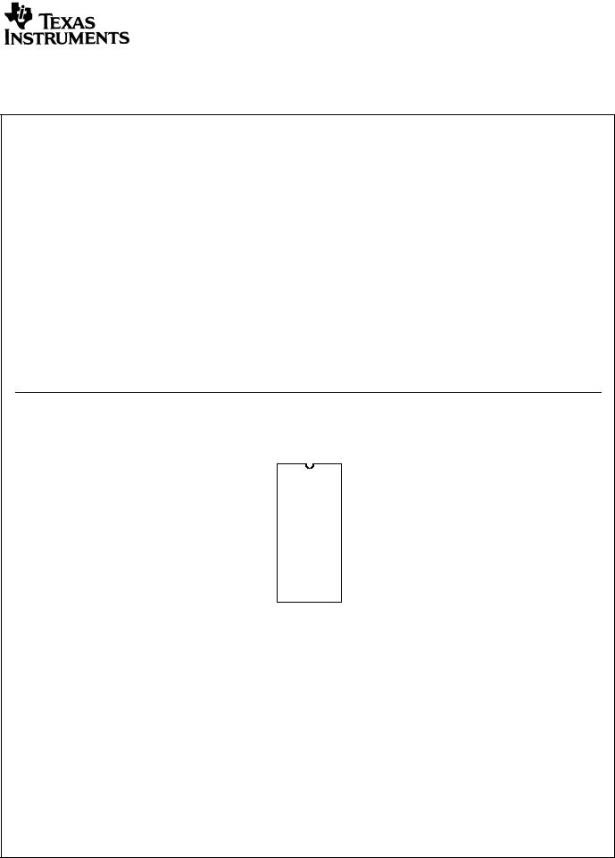
Pinout
CD74HC10, CD74HCT10
(PDIP, SOIC)
TOP VIEW
1A |
1 |
|
14 |
VCC |
1B |
|
|
|
1C |
2 |
|
13 |
||
2A |
|
|
|
1Y |
3 |
|
12 |
||
2B |
|
|
|
3C |
4 |
|
11 |
||
2C |
|
|
|
3B |
5 |
|
10 |
||
2Y |
|
|
|
3A |
6 |
|
9 |
||
GND |
|
|
|
3Y |
7 |
|
8 |
CAUTION: These devices are sensitive to electrostatic discharge. Users should follow proper IC Handling Procedures. |
File Number 1551.1 |
|
|
||
Copyright © Harris Corporation 1997 |
1 |
|
|
|
|

CD74HC10, CD74HCT10
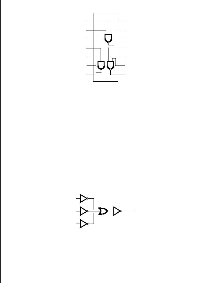
Functional Diagram
1 |
14 |
1A |
VCC |
2 |
13 |
1B |
1C |
3 |
12 |
2A |
1Y |
4 |
11 |
2B |
3C |
5 |
10 |
2C |
3B |
6 |
9 |
2Y |
3A |
7 |
8 |
GND |
3Y |
TRUTH TABLE
|
INPUTS |
|
OUTPUT |
|
|
|
|
nA |
nB |
nC |
nY |
|
|
|
|
L |
L |
L |
H |
|
|
|
|
L |
L |
H |
H |
|
|
|
|
L |
H |
L |
H |
|
|
|
|
L |
H |
H |
H |
|
|
|
|
H |
L |
L |
H |
|
|
|
|
H |
L |
H |
H |
|
|
|
|
H |
H |
L |
H |
|
|
|
|
H |
H |
H |
L |
|
|
|
|
NOTE: H = High Voltage Level, L = Low Voltage Level
Logic Symbol
nA
nB |
nY |
nC
2
 Loading...