


CD74ACT86M96
Texas Instruments CD74ACT86M96, CD74ACT86M, CD74ACT86E, CD74AC86M, CD74AC86E Datasheet
...
1
Data sheet acquired from Harris Semiconductor
SCHS232A
Features
• Buffered Inputs
• Typical Propagation Delay
- 3.2ns at V
CC
= 5V, T
A
= 25
o
C, C
L
= 50pF
• Exceeds 2kV ESD Protection MIL-STD-883, Method
3015
• SCR-Latchup-Resistant CMOS Process and Circuit
Design
• Speed of Bipolar FAST™/AS/S with Significantly
Reduced Power Consumption
• Balanced Propagation Delays
• AC Types Feature 1.5V to 5.5V Operation and
Balanced Noise Immunity at 30% of the Supply
• ±24mA Output Drive Current
- Fanout to 15 FAST™ ICs
- Drives 50Ω Transmission Lines
Description
The CD74AC86 and ’ACT86 are quad 2-input Exclusive-OR
gates that utilize Advanced CMOS Logic technology
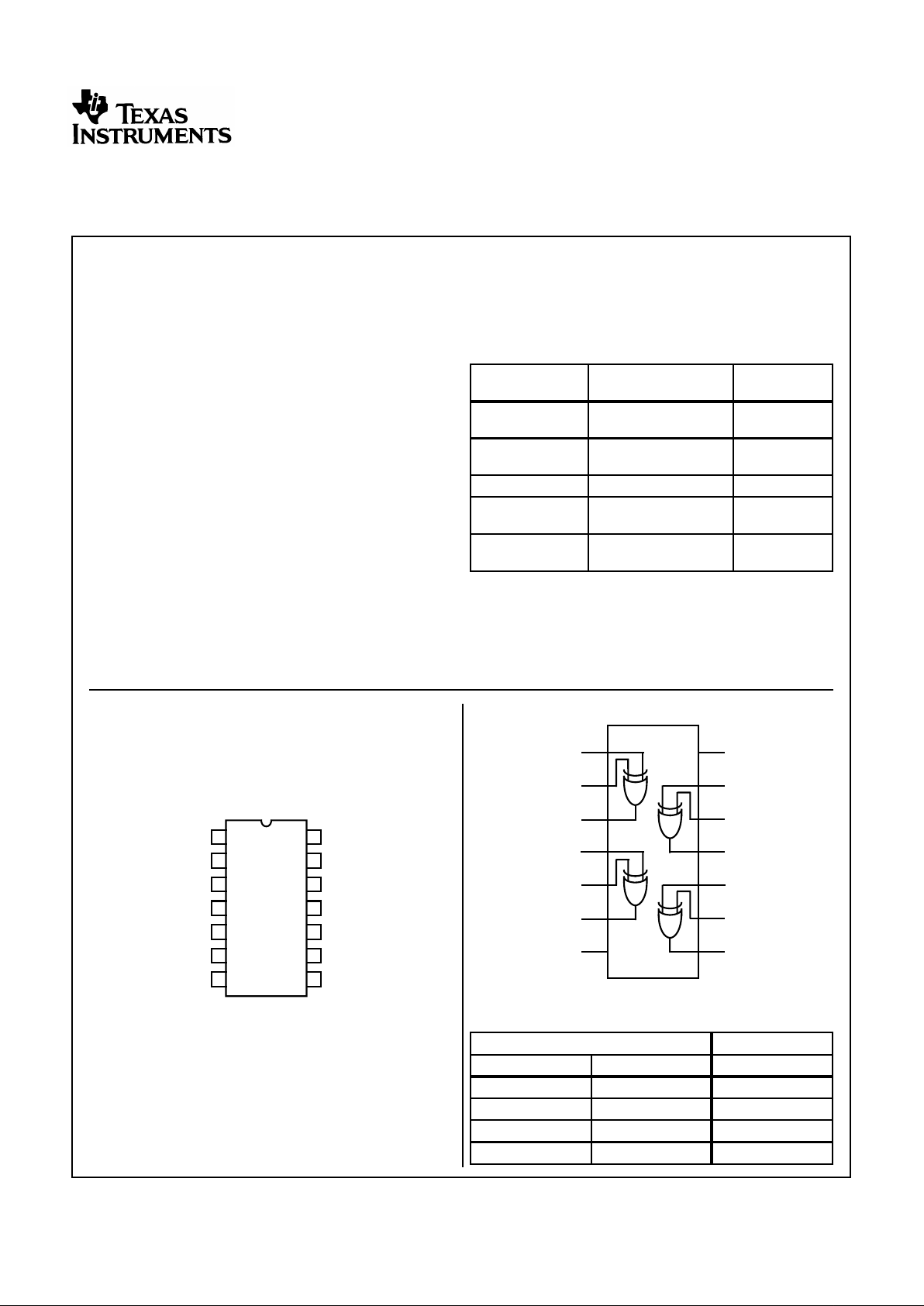
Pinout
CD54ACT86
(CERDIP)
CD74AC86, CD74ACT86
(PDIP, SOIC)
TOP VIEW
Functional Diagram
Ordering Information
PART
NUMBER TEMP. RANGE (
o
C) PACKAGE
CD74AC86E 0 to 70
o
C, -40 to 85,
-55 to 125
14 Ld PDIP
CD74AC86M 0 to 70
o
C, -40 to 85,
-55 to 125
14 Ld SOIC
CD54ACT86F3A -55 to 125 14 Ld CERDIP
CD74ACT86E 0 to 70
o
C, -40 to 85,
-55 to 125
14 Ld PDIP
CD74ACT86M 0 to 70
o
C, -40 to 85,
-55 to 125
14 Ld SOIC
NOTES:
1. When ordering, use the entire part number. Add the suffix 96 to
obtain the variant in the tape and reel.
2. Waf erand die for this partnumber is available which meets all
electrical specifications. Please contact your local TI sales office or
customer service for ordering information.
1A
1B
1Y
2A
2B
2Y
GND
V
CC
4B
4A
4Y
3B
3A
3Y
1
2
3
4
5
6
7
14
13
12
11
10
9
8
TRUTH TABLE
INPUTS OUTPUT
nA nB nY
LLL
HHL
HLH
LHH
1A
1B
2A
2B
2Y
GND
1
2
3
4
5
6
14
13
12
11
V
CC
4Y
3Y
3B
4A
4B
10
8
7
9
3A
1Y
September 1998 - Revised May 2000
CAUTION: These devices are sensitive to electrostatic discharge. Users should follow proper IC Handling Procedures.
FAST™ is a Trademark of Fairchild Semiconductor.
Copyright
© 2000, Texas Instruments Incorporated
CD74AC86,
CD54/74ACT86
Quad 2-Input Exclusive-OR Gate
[ /Title
(CD74
AC86,
CD74
ACT86
)
/
Sub-
j
ect
(Quad
2-Input
Exclu-
sive-
OR
Gate)
/
Autho
r ()
/
Key-
words
(Har-
ris
Semi-
con-
ductor,
Advan
ced
CMOS
,Harris
Semi-
con-
ductor,
Advan
ced
TTL)
/
Cre-
ator ()
/
DOCI
NFO
pdf-
2
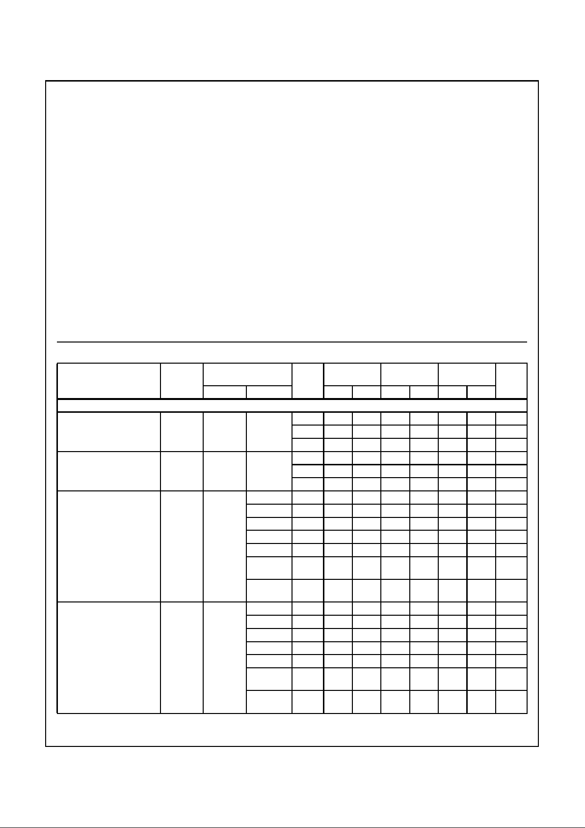
Absolute Maximum Ratings Thermal Information
DC Supply Voltage, V
CC
. . . . . . . . . . . . . . . . . . . . . . . . -0.5V to 6V
DC Input Diode Current, I
IK
For V
I
< -0.5V or V
I
> V
CC
+ 0.5V. . . . . . . . . . . . . . . . . . . . . .±20mA
DC Output Diode Current, I
OK
For V
O
< -0.5V or V
O
> V
CC
+ 0.5V . . . . . . . . . . . . . . . . . . . .±50mA
DC Output Source or Sink Current per Output Pin, I
O
For V
O
> -0.5V or V
O
< V
CC
+ 0.5V . . . . . . . . . . . . . . . . . . . .±50mA
DC V
CC
or Ground Current, I
CC or
I
GND
(Note 3) . . . . . . . . .±100mA
Operating Conditions
Temperature Range, T
A
. . . . . . . . . . . . . . . . . . . . . . -55
o
C to 125
o
C
Supply Voltage Range, V
CC
(Note 4). . . . . . . . . . . . . . .4.5V to 5.5V
DC Input or Output Voltage, V
I
, V
O
. . . . . . . . . . . . . . . . . 0V to V
CC
Input Rise and Fall Slew Rate, dt/dv
4.5V to 5.5V . . . . . . . . . . . . . . . . . . . . . . . . . . . . . . . . 10ns (Max)
Thermal Resistance (Typical, Note 5) θ
JA
(
o
C/W)
PDIP Package. . . . . . . . . . . . . . . . . . . . . . . . . . . . . 90
SOIC Package. . . . . . . . . . . . . . . . . . . . . . . . . . . . . 175
Maximum Junction Temperature (Plastic Package) . . . . . . . . . . 150
o
C
Maximum Storage Temperature Range . . . . . . . . . .-65
o
C to 150
o
C
Maximum Lead Temperature (Soldering 10s) . . . . . . . . . . . . . 300
o
C
CAUTION: Stresses above those listed in “Absolute Maximum Ratings” may cause permanent damage to the device. This is a stress only rating and operation
of the device at these or any other conditions above those indicated in the operational sections of this specification is not implied.
NOTES:
3. For up to 4 outputs per device, add ±25mA for each additional output.
4. Unless otherwise specified, all voltages are referenced to ground.
5. θ
JA
is measured with the component mounted on an evaluation PC board in free air.
DC Electrical Specifications
PARAMETER SYMBOL
TEST
CONDITIONS
V
CC
(V)
25
o
C
-40
o
C TO
85
o
C
-55
o
C TO
125
o
C
UNITSV
I
(V) I
O
(mA) MIN MAX MIN MAX MIN MAX
AC TYPES
High Level Input Voltage V
IH
- - 1.5 1.2 - 1.2 - 1.2 - V
3 2.1 - 2.1 - 2.1 - V
5.5 3.85 - 3.85 - 3.85 - V
Low Level Input Voltage V
IL
- - 1.5 - 0.3 - 0.3 - 0.3 V
3 - 0.9 - 0.9 - 0.9 V
5.5 - 1.65 - 1.65 - 1.65 V
High Level Output Voltage V
OH
V
IH
or V
IL
-0.05 1.5 1.4 - 1.4 - 1.4 - V
-0.05 3 2.9 - 2.9 - 2.9 - V
-0.05 4.5 4.4 - 4.4 - 4.4 - V
-4 3 2.58 - 2.48 - 2.4 - V
-24 4.5 3.94 - 3.8 - 3.7 - V
-75
(Note 6, 7)
5.5 - - 3.85 - - - V
-50
(Note 6, 7)
5.5----3.85 - V
Low Level Output Voltage V
OL
V
IH
or V
IL
0.05 1.5 - 0.1 - 0.1 - 0.1 V
0.05 3 - 0.1 - 0.1 - 0.1 V
0.05 4.5 - 0.1 - 0.1 - 0.1 V
12 3 - 0.36 - 0.44 - 0.5 V
24 4.5 - 0.36 - 0.44 - 0.5 V
75
(Note 6, 7)
5.5 - - - 1.65 - - V
50
(Note 6, 7)
5.5-----1.65 V
CD74AC86, CD54/74ACT86
 Loading...