


CD74HCT132E
Texas Instruments CD74HCT132E, CD74HCT132M96, CD74HCT132M, CD74HC132M96, CD74HC132M Datasheet
...
1
Data sheet acquired from Harris Semiconductor
SCHS145
Features
• Unlimited Input Rise and Fall Times
• Exceptionally High Noise Immunity
• Typical Propagation Delay: 10ns at V
CC
= 5V,
C
L
= 15pF, T
A
= 25
o
C
• Fanout (Over Temperature Range)
- Standard Outputs. . . . . . . . . . . . . . . 10 LSTTL Loads
- Bus Driver Outputs . . . . . . . . . . . . . 15 LSTTL Loads
• Wide Operating Temperature Range . . . -55
o
C to 125
o
C
• Balanced Propagation Delay and Transition Times
• Significant Power Reduction Compared to LSTTL
Logic ICs
• HC Types
- 2V to 6V Operation
- High Noise Immunity: N
IL
= 37%, N
IH
= 51% of V
CC
at V
CC
= 5V
• HCT Types
- 4.5V to 5.5V Operation
- Direct LSTTL Input Logic Compatibility,
V
IL
= 0.8V (Max), V
IH
= 2V (Min)
- CMOS Input Compatibility, I
l
≤ 1µA at V
OL
, V
OH
• Related Literature
- CD54HC132F3A and CD54HCT132F3A Military
Data Sheet, Document Number 3778
Description
The Harris CD74HC132, CD74HCT132 each contain four
2-input NAND Schmitt Triggers in one package. This logic
device utilizes silicon gate CMOS technology to achieve
operating speeds similar to LSTTL gates with the low power
consumption of standard CMOS integrated circuits. All
devices have the ability to drive 10 LSTTL loads. The 74HCT
Pinout
CD74HC132, CD74HCT132
(PDIP, SOIC)
TOP VIEW
1A
1B
1Y
2A
2B
2Y
GND
V
CC
4B
4A
4Y
3B
3A
3Y
1
2
3
4
5
6
7
14
13
12
11
10
9
8
August 1997
CAUTION: These devices are sensitive to electrostatic discharge. Users should follow proper IC Handling Procedures.
Copyright
© Harris Corporation 1997
CD74HC132,
CD74HCT132
High Speed CMOS Logic
Quad 2-Input NAND Schmitt Trigger
File Number 1649.1
[ /Title
(CD74
HC132
,
CD74
HCT13
2)
/
Sub-
j
ect
(High
Speed
CMOS
Logic
Quad
2-Input
NAND
Schmit
2
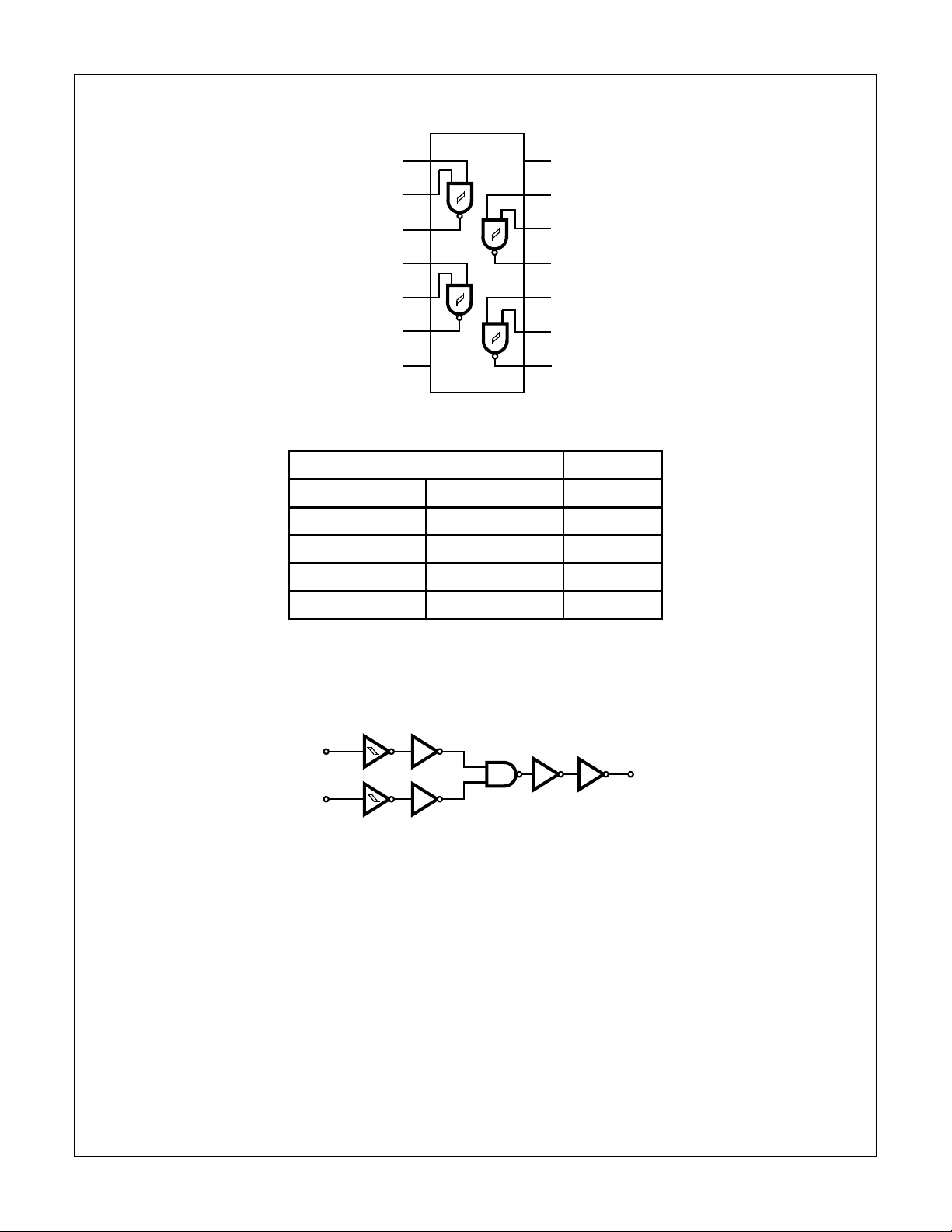
Functional Diagram
Logic Symbol
TRUTH TABLE
INPUTS OUTPUT
nA nB nY
LLH
LHH
HLH
HHL
NOTE: H = High Voltage Level, L = Low Voltage Level
1A
1B
2A
2B
2Y
GND
1
2
3
4
5
6
14
13
12
11
V
CC
4B
3Y
3B
4A
4Y
10
8
7
9
3A
1Y
nA
nB
nY
CD74HC132, CD74HCT132
3
Absolute Maximum Ratings Thermal Information
DC Supply Voltage, V
CC
. . . . . . . . . . . . . . . . . . . . . . . . -0.5V to 7V
DC Input Diode Current, I
IK
For V
I
< -0.5V or V
I
> V
CC
+ 0.5V. . . . . . . . . . . . . . . . . . . . . .±20mA
DC Output Diode Current, I
OK
For V
O
< -0.5V or V
O
> V
CC
+ 0.5V . . . . . . . . . . . . . . . . . . . .±20mA
DC Output Source or Sink Current per Output Pin, I
O
For V
O
> -0.5V or V
O
< V
CC
+ 0.5V . . . . . . . . . . . . . . . . . . . .±25mA
DC V
CC
or Ground Current, I
CC or
I
GND
. . . . . . . . . . . . . . . . . .±50mA
Operating Conditions
Temperature Range (T
A
) . . . . . . . . . . . . . . . . . . . . . -55
o
C to 125
o
C
Supply Voltage Range, V
CC
HC Types . . . . . . . . . . . . . . . . . . . . . . . . . . . . . . . . . . . . .2V to 6V
HCT Types . . . . . . . . . . . . . . . . . . . . . . . . . . . . . . . . .4.5V to 5.5V
DC Input or Output Voltage, V
I
, V
O
. . . . . . . . . . . . . . . . . 0V to V
CC
Input Rise and Fall Time
2V . . . . . . . . . . . . . . . . . . . . . . . . . . . . . . . . . . . . . . . 100ms (Max)
4.5V. . . . . . . . . . . . . . . . . . . . . . . . . . . . . . . . . . . . . . 100ms (Max)
6V . . . . . . . . . . . . . . . . . . . . . . . . . . . . . . . . . . . . . . . 100ms (Max)
Thermal Resistance (Typical, Note 3) θ
JA
(
o
C/W)
PDIP Package. . . . . . . . . . . . . . . . . . . . . . . . . . . . . 90
SOIC Package. . . . . . . . . . . . . . . . . . . . . . . . . . . . . 175
Maximum Junction Temperature. . . . . . . . . . . . . . . . . . . . . . .150
o
C
Maximum Storage Temperature Range . . . . . . . . . .-65
o
C to 150
o
C
Maximum Lead Temperature (Soldering 10s). . . . . . . . . . . . .300
o
C
(SOIC - Lead Tips Only)
CAUTION: Stresses above those listed in “Absolute Maximum Ratings” may cause permanent damage to the device. This is a stress only rating and operation
of the device at these or any other conditions above those indicated in the operational sections of this specification is not implied.
NOTE:
3. θ
JA
is measured with the component mounted on an evaluation PC board in free air.
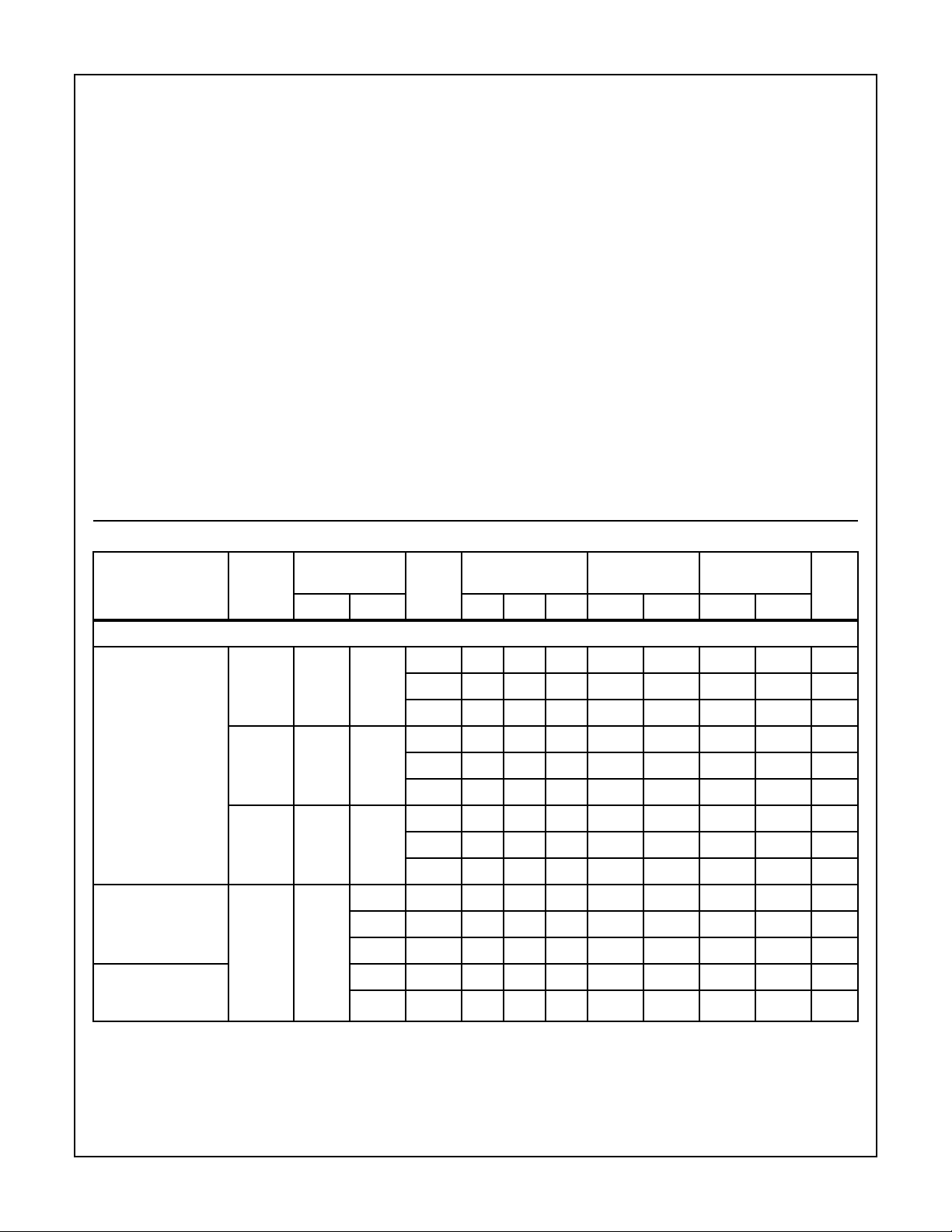
DC Electrical Specifications
PARAMETER SYMBOL
TEST
CONDITIONS
V
CC
(V)
25
o
C -40
o
C TO 85
o
C -55
o
C TO 125
o
C
UNITSV
I
(V) I
O
(mA) MIN TYP MAX MIN MAX MIN MAX
HC TYPES
Input Switch Points
(Note 6)
V
T
+ - - 2 0.7 - 1.5 0.7 1.5 0.7 1.5 V
4.5 1.7 - 3.15 1.7 3.15 1.7 3.15 V
6 2.1 - 4.2 2.1 4.2 2.1 4.2 V
V
T
- - - 2 0.3 - 1 0.3 1 0.3 1 V
4.5 0.9 - 2.2 0.9 2.2 0.9 2.2 V
6 1.2 - 3 1.2 3 1.2 3 V
V
H
2 0.2 - 1 0.2 1 0.2 1 V
4.5 0.4 - 1.4 0.4 1.4 0.4 1.4 V
6 0.6 - 1.6 0.6 1.6 0.6 1.6 V
High Level Output
Voltage
CMOS Loads
V
OH
V
T
+ or
V
T
-
-0.02 2 1.9 - - 1.9 - 1.9 - V
-0.02 4.5 4.4 - - 4.4 - 4.4 - V
-0.02 6 5.9 - - 5.9 - 5.9 - V
High Level Output
Voltage
TTL Loads
-4 4.5 3.98 - - 3.84 - 3.7 - V
-5.2 6 5.48 - - 5.34 - 5.2 - V
CD74HC132, CD74HCT132
 Loading...