Texas Instruments CD74HC7266M96, CD74HC7266M, CD74HC7266E, CD54HC7266F3A, 8404302CA Datasheet

Data sheet acquired from Harris Semiconductor SCHS219
August 1997
CD74HC7266
High Speed CMOS Logic
Quad 2-Input EXCLUSIVE NOR Gate
[ /Title (CD74H C7266) /Subject (High Speed CMOS Logic Quad 2- Input EXCLUSIVE
Features
•Four Independent EXCLUSIVE NOR Gates
•Buffered Inputs and Outputs
•Logical Comparators
•Parity Generators and Checkers
•Adders/Subtracters
•Fanout (Over Temperature Range)
-Standard Outputs . . . . . . . . . . . . . . . 10 LSTTL Loads
-Bus Driver Outputs . . . . . . . . . . . . . 15 LSTTL Loads
•Wide Operating Temperature Range . . . -55oC to 125oC
•Balanced Propagation Delay and Transition Times
•Significant Power Reduction Compared to LSTTL Logic ICs
•HC Types
-2V to 6V Operation
-High Noise Immunity: NIL = 30%, NIH = 30%of VCC at VCC = 5V
Description
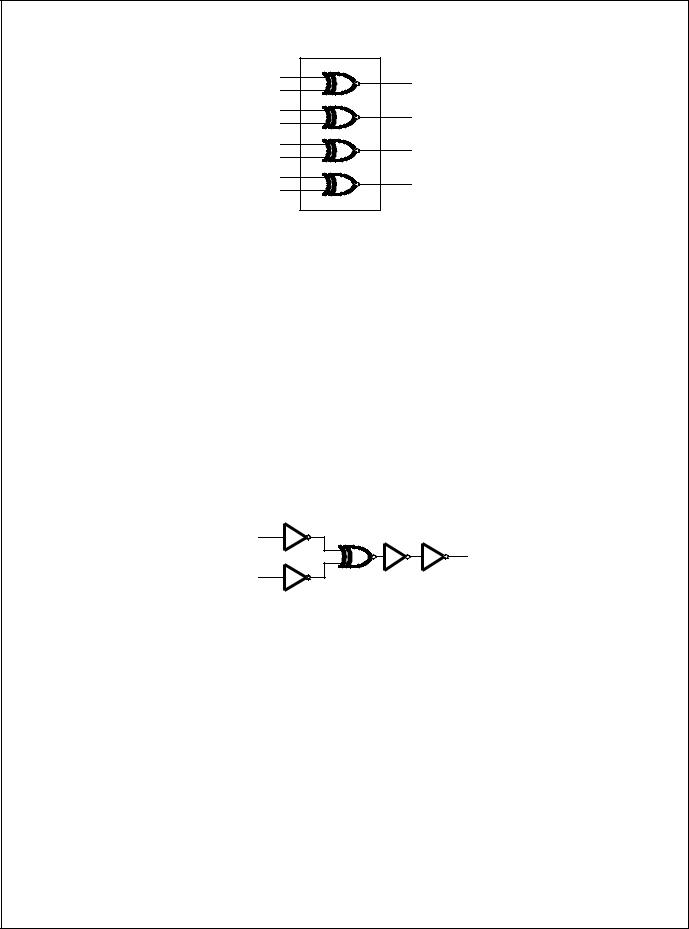
The Harris CD74HC7266 contains four independent Exclusive NOR gates in one package. They provide the system designer with a means for implementation of the EXCLUSIVE NOR function.
This device is functionally the same as the TTL226. They differ in that the HC7266 has active high and low outputs whereas the 226 has open collector outputs.
Ordering Information
|
TEMP. RANGE (oC) |
|
PKG. |
PART NUMBER |
PACKAGE |
NO. |
|
CD74HC7266E |
-55 to 125 |
14 Ld PDIP |
E14.3 |
|
|
|
|
CD74HC7266M |
-55 to 125 |
14 Ld SOIC |
M14.15 |
|
|
|
|
NOTES: |
|
|
|
1.When ordering, use the entire part number. Add the suffix 96 to obtain the variant in the tape and reel.
2.Die for this part number is available which meets all electrical specifications. Please contact your local sales office or Harris customer service for ordering information.
Pinout
CD74HC7266 (PDIP, SOIC)
TOP VIEW
1A |
1 |
|
14 |
VCC |
1B |
|
|
|
4B |
2 |
|
13 |
||
1Y |
|
|
|
4A |
3 |
|
12 |
||
2Y |
|
|
|
4Y |
4 |
|
11 |
||
2A |
|
|
|
3Y |
5 |
|
10 |
||
2B |
|
|
|
3B |
6 |
|
9 |
||
GND |
|
|
|
3A |
7 |
|
8 |
CAUTION: These devices are sensitive to electrostatic discharge. Users should follow proper IC Handling Procedures. |
File Number 1780.1 |
|
|
||
Copyright © Harris Corporation 1997 |
1 |
|
|
|
|

CD74HC7266
Functional Diagram
1A |
1 |
3 |
|
2 |
|||
1B |
1Y |
||
|
|
||
2A |
5 |
4 |
|
|
|||
2B |
6 |
2Y |
|
|
|
||
3A |
8 |
10 |
|
9 |
|||
3B |
3Y |
||
|
|
||
4A |
12 |
11 |
|
|
|||
13 |
4Y |
||
4B |
|||
|
|||
|
GND = 7 |
||
|
|
||
|
|
VCC = 14 |
TRUTH TABLE
|
INPUTS |
OUTPUT |
|
|
|
|
|
nA |
|
nB |
nY |
|
|
|
|
L |
|
L |
H |
|
|
|
|
L |
|
H |
L |
|
|
|
|
H |
|
L |
L |
|
|
|
|
H |
|
H |
H |
|
|
|
|
NOTE: H = High Voltage Level, L = Low Voltage Level
Logic Symbol
nA
nY
nB
2
 Loading...