Texas Instruments DS3680DR, DS3680D, DS3680N Datasheet

DS3680 QUAD TELEPHONE RELAY DRIVER
SLRS014C ± MARCH 1986 ± REVISED SEPTEMBER 1995
•Designed for ±52-V Battery Operation
•50-mA Output Current Capability
•Input Compatible With TTL and CMOS
•High Common-Mode Input Voltage Range
•Very Low Input Current
•Fail-Safe Disconnect Feature
•Built-in Output Clamp Diode
•Direct Replacement for National DS3680 and Fairchild A3680
description
D OR N PACKAGE
(TOP VIEW)
1 IN+ |
|
1 |
14 |
|
BAT GND |
|
|
||||
1 IN± |
|
2 |
13 |
|
1 OUT |
|
|
||||
2 IN± |
|
3 |
12 |
|
2 OUT |
|
|
||||
2 IN+ |
|
4 |
11 |
|
3 OUT |
|
|
||||
3 IN+ |
|
5 |
10 |
|
4 OUT |
|
|
||||
3 IN± |
|
6 |
9 |
|
BAT NEG |
|
|
||||
4 IN± |
|
7 |
8 |
|
4 IN+ |
|
|
||||
|
|
|
|
|
|
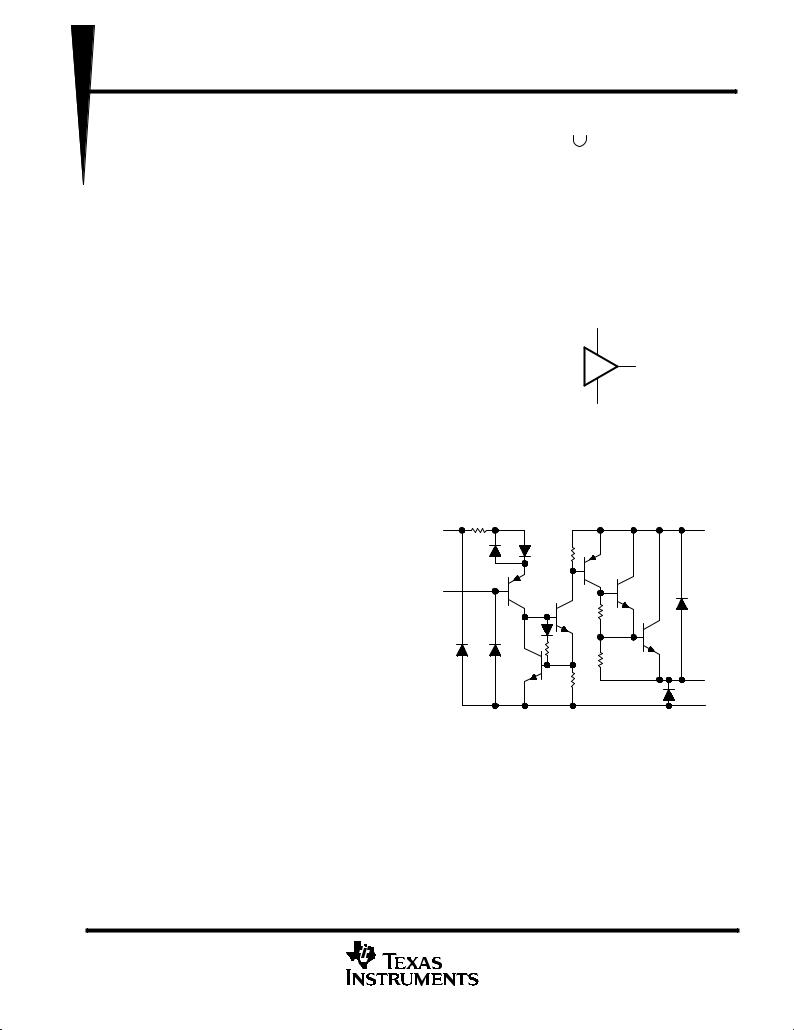
symbol (each driver)
The DS3680 telephone relay driver is a monolithic integrated circuit designed to interface ±48-V relay systems to TTL or other systems in telephone applications. It is capable of sourcing up to 50 mA from standard ±52-V battery power. To reduce the effects of noise and IR drop between logic ground and battery ground, these drivers are designed to operate with a common-mode input range of ± 20 V referenced to battery ground. The common-mode input voltages for the four drivers can be different, so a wide range of input elements can be accommodated. The high-impedance inputs are compatible with positive TTL and CMOS levels or negative logic levels. A clamp network is included in the driver outputs to limit high-voltage transients generated by the relay coil during switching. The complementary inputs ensure that the driver output is off as a fail-safe condition when either output is open.
The DS3680 is characterized for operation from 0°C to 70°C.
|
|
BAT GND |
||
|
|
|
|
|
IN + |
|
|
+ |
OUT |
|
|
|||
|
|
|
± |
|
IN ± |
|
|
|
|
|
|
|||
|
|
|
||
|
|
|
|
|
|
|
BAT NEG |
|
|
|
|
|
|
|
schematic diagram (each driver)
IN + |
15 kΩ |
BAT GND |
|
IN ±
OUT
BAT NEG
All resistor values shown are nominal.
PRODUCTION DATA information is current as of publication date. Products conform to specifications per the terms of Texas Instruments standard warranty. Production processing does not necessarily include testing of all parameters.
Copyright 1995, Texas Instruments Incorporated
POST OFFICE BOX 655303 •DALLAS, TEXAS 75265 |
1 |

DS3680
QUAD TELEPHONE RELAY DRIVER
SLRS014C ± MARCH 1986 ± REVISED SEPTEMBER 1995
absolute maximum ratings over operating free-air temperature range (unless otherwise noted)
Supply voltage range at BAT NEG, VBAT ± (see Note 1) . . . . . . . . . . . . . . . . . . . . |
. . . . . . . . . . . . ±70 V to 0.5 V |
|
Input voltage range with respect to BAT GND . . . . . . . . . . . . . . . . . . . . . . . . . . . . . . |
. . . . . . . . . . . ±70 V to 20 |
V |
Input voltage range with respect to BAT NEG . . . . . . . . . . . . . . . . . . . . . . . . . . . . . . |
. . . . . . . . . . . ±0.5 V to 70 |
V |
Differential input voltage, VID (see Note 2) . . . . . . . . . . . . . . . . . . . . . . . . . . . . . . . . |
. . . . . . . . . . . . . . . . . . ± 20 |
V |
Output current, IO: Resistive load . . . . . . . . . . . . . . . . . . . . . . . . . . . . . . . . . . . . . . . |
. . . . . . . . . . . . . . . ±100 mA |
|
Inductive load . . . . . . . . . . . . . . . . . . . . . . . . . . . . . . . . . . . . . . . |
. . . . . . . . . . . . . . . . ±50 mA |
|
Inductive output load . . . . . . . . . . . . . . . . . . . . . . . . . . . . . . . . . . . . . . . . . . . . . . . . . . . |
. . . . . . . . . . . . . . . . . . . . 5 H |
|
Continuous total dissipation . . . . . . . . . . . . . . . . . . . . . . . . . . . . . . . . . . . . . . . . . . . |
See Dissipation Rating Table |
|
Operating free-air temperature range, TA . . . . . . . . . . . . . . . . . . . . . . . . . . . . . . . . . |
. . . . . . . . . . . . . 0°C to 70°C |
|
Storage temperature range, Tstg . . . . . . . . . . . . . . . . . . . . . . . . . . . . . . . . . . . . . . . . . |
. . . . . . . . . ±65°C to 150°C |
|
Lead temperature 1,6 mm (1/16 inch) from case for 60 seconds . . . . . . . . . . . . . |
. . . . . . . . . . . . . . . . . . 260°C |
|
NOTES: 1. All voltages are with respect to BAT GND, unless otherwise specified.
2. Differential input voltages are at the noninverting input terminal IN + with respect to the inverting input terminal IN ±.
|
DISSIPATION RATING TABLE |
|
||
PACKAGE |
TA ≤ 25°C |
DERATING FACTOR |
TA = 70°C |
|
POWER RATING |
ABOVE TA = 25°C |
POWER RATING |
||
|
||||
D |
950 mW |
7.6 mW/°C |
608 mW |
|
N |
1150 mW |
9.2 mW/°C |
736 mW |
|
|
|
|
|
|
recommended operating conditions
|
MIN |
MAX |
UNIT |
|
|
|
|
Supply voltage, VBAT ± |
± 10 |
± 60 |
V |
Input voltage, either input |
± 20² |
20 |
V |
High-level differential input voltage, VIDH |
2 |
20 |
V |
Low-level differential input voltage, VIDL |
± 20² |
0.8 |
V |
Operating free-air temperature, TA |
0 |
70 |
°C |
² The algebraic convention, in which the less positive (more negative) limit is designated minimum, is used in this data sheet for input voltage levels.
electrical characteristics over recommended operating free-air temperature range, VBAT± = ±52 V (unless otherwise noted)
|
PARAMETER |
TEST CONDITIONS |
MIN TYP³ |
MAX |
UNIT |
||
IIH |
High-level input current (into IN + ) |
VID = 2 V |
|
40 |
100 |
A |
|
VID = 7 V |
|
375 |
1000 |
||||
|
|
|
|
||||
IIL |
Low-level input current (into IN + ) |
VID = 0.4 V |
|
0.01 |
5 |
A |
|
VID = ± 7 V |
|
± 1 |
± 100 |
||||
|
|
|
|
||||
VO(on) |
On-stage output voltage |
IO = 50 mA, |
VID = 2 V |
± 1.6 |
± 2.1 |
V |
|
IO(off) |
Off-stage output current |
VO = VBAT ± |
VID = 0.8 V |
± 2 |
± 100 |
A |
|
Inputs open |
± 2 |
± 100 |
|||||
|
|
|
|
||||
|
|
|
|
|
|
|
|
IR |
Clamp diode reverse current |
VO = 0 |
|
2 |
100 |
A |
|
VOK |
Output clamp voltage |
IO = 50 mA |
|
0.9 |
1.2 |
V |
|
IO = ± 50 mA, |
VBAT ± = 0 |
± 0.9 |
± 1.2 |
||||
|
|
|
|||||
IBAT(on) |
On-state battery current |
All drivers on |
|
± 2 |
± 4.4 |
mA |
|
IBAT(off) |
Off-state battery current |
All drivers off |
|
± 1 |
± 100 |
A |
|
³ All typical values are at TA = 25°C.
2 |
POST OFFICE BOX 655303 •DALLAS, TEXAS 75265 |
 Loading...