


 Loading...
PRODUCT |
Sample & |
TECHNICAL |
TOOLS & |
Support & |
FOLDER |
Buy |
DOCUMENTS |
SOFTWARE |
Community |
DRV134, DRV135
SBOS094B –JANUARY 1998–REVISED DECEMBER 2014
DRV13x Audio-Balanced Line Drivers
1 Features
•Balanced Output
•Low Distortion: 0.0005% at f = 1 kHz
•Wide Output Swing: 17Vrms into 600 Ω
•High Capacitive Load Drive
•High Slew Rate: 15 V/µs
•Wide Supply Range: ±4.5 V to ±18 V
•Low Quiescent Current: ±5.2 mA
•8-Pin DIP, SO-8, and SOL-16 Packages
•Companion to Audio Differential Line Receivers: INA134 and INA137
•Improved Replacement for SSM2142
2 Applications
•Audio Differential Line Drivers
•Audio Mix Consoles
•Distribution Amplifiers
•Graphic and Parametric Equalizers
•Dynamic Range Processors
•Digital Effects Processors
•Telecom Systems
•Hi-Fi Equipment
•Industrial Instrumentation
4 Simplified Schematic
3 Description
The DRV134 and DRV135 are differential output amplifiers that convert a single-ended input to a balanced output pair. These balanced audio drivers consist of high performance op amps with on-chip precision resistors. They are fully specified for high performance audio applications and have excellent ac specifications, including low distortion (0.0005% at 1 kHz) and high slew rate (15 V/µs).
The on-chip resistors are laser-trimmed for accurate gain and optimum output common-mode rejection. Wide output voltage swing and high output drive capability allow use in a wide variety of demanding applications. They easily drive the large capacitive loads associated with long audio cables. Used in combination with the INA134 or INA137 differential receivers, they offer a complete solution for transmitting analog audio signals without degradation.
The DRV134 is available in 8-pin DIP and SOL-16 surface-mount packages. The DRV135 comes in a space-saving SO-8 surface-mount package. Both are specified for operation over the extended industrial temperature range, –40°C to +85°C and operate from –55°C to +125°C.
Device Information(1)
PART NUMBER |
PACKAGE |
BODY SIZE (NOM) |
DRV134 |
SOIC (16) |
10.30 mm × 7.50 mm |
DRV135 |
SOIC (8) |
4.90 mm × 3.91 mm |
(1)For all available packages, see the orderable addendum at the end of the datasheet.
|
V+ |
|
|
|
50Ω |
|
A2 |
+VO |
|
|
+SENSE |
|
|
10KΩ |
|
|
–SENSE |
VIN |
|
|
|
A1 |
50Ω |
GND |
A3 |
–VO |
|
||
|
|
10KΩ |
|
ALL RESISTORS 30KΩ UNLESS OTHERWISE INDICATED. |
|
|
V– |
|
An IMPORTANT NOTICE at the end of this data sheet addresses availability, warranty, changes, use in safety-critical applications, intellectual property matters and other important disclaimers. PRODUCTION DATA.

DRV134, DRV135
SBOS094B –JANUARY 1998 –REVISED DECEMBER 2014 www.ti.com
Table of Contents
1 |
Features .................................................................. |
1 |
|
8.4 |
Device Functional Modes........................................ |
13 |
|
2 |
Applications ........................................................... |
1 |
9 |
Application and Implementation ........................ |
15 |
||
3 |
Description ............................................................. |
1 |
|
9.1 |
Application Information............................................ |
15 |
|
4 |
Simplified Schematic............................................. |
1 |
|
9.2 |
Typical Application ................................................. |
15 |
|
5 |
Revision History..................................................... |
2 |
10 |
Power Supply Recommendations ..................... |
17 |
||
6 |
Pin Configuration and Functions ......................... |
3 |
11 |
Layout................................................................... |
17 |
||
7 |
Specifications |
4 |
|
11.1 |
Layout Guidelines ................................................. |
17 |
|
|
11.2 |
Layout Examples |
18 |
||||
|
7.1 |
Absolute Maximum Ratings |
4 |
|
|||
|
|
11.3 |
Thermal Performance |
19 |
|||
|
7.2 |
Handling Ratings |
4 |
|
|||
|
12 Device and Documentation Support |
19 |
|||||
|
7.3 |
Recommended Operating Conditions ...................... |
4 |
||||
|
7.4 |
Electrical Characteristics |
5 |
|
12.1 |
Documentation Support ........................................ |
19 |
|
|
12.2 |
Related Links |
19 |
|||
|
7.5 |
Typical Characteristics |
6 |
|
|||
|
|
12.3 |
Trademarks |
19 |
|||
8 |
Detailed Description |
11 |
|
||||
|
12.4 |
Electrostatic Discharge Caution |
19 |
||||
|
8.1 |
Overview |
11 |
|
|||
|
|
12.5 |
Glossary |
19 |
|||
|
8.2 |
Functional Block Diagram |
11 |
|
|||
|
13 Mechanical, Packaging, and Orderable |
|
|||||
|
8.3 |
Feature Description................................................. |
11 |
20 |
|||
|
|
|
|
|
Information ........................................................... |
||
|
|
|
|
|
|
|
|
5 Revision History
Changes from Revision A (April 2007) to Revision B Page
•Added Handling Rating table, Feature Description section, Device Functional Modes, Application and Implementation section, Power Supply Recommendations section, Layout section, Device and Documentation
Support section, and Mechanical, Packaging, and Orderable Information section ............................................................... |
1 |
2 |
Submit Documentation Feedback |
Copyright © 1998–2014, Texas Instruments Incorporated |
Product Folder Links: DRV134 DRV135
|
|
|
|
|
|
|
|
DRV134, DRV135 |
www.ti.com |
|
|
|
|
SBOS094B –JANUARY 1998 –REVISED DECEMBER 2014 |
|||
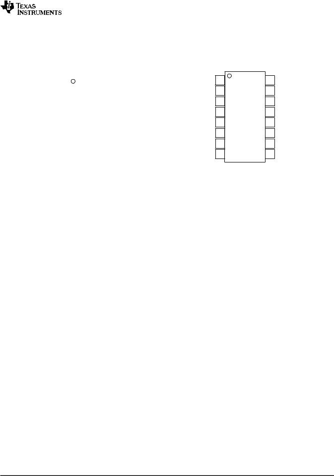
6 Pin Configuration and Functions |
|
|
|
|
||||
TOP VIEW |
|
8-PIN DIP/SO-8 |
TOP VIEW |
SOL-16 |
||||
|
|
|
|
+VO |
NC |
1 |
16 |
NC |
|
|
|
|
|||||
–VO |
1 |
|
8 |
NC |
2 |
15 |
NC |
|
–SENSE |
|
|
|
+SENSE |
||||
|
|
|
||||||
2 |
|
7 |
|
|
|
|
||
GND |
|
|
|
V+ |
–VO |
3 |
14 |
+VO |
|
|
|
||||||
3 |
|
6 |
|
|
|
|
||
VIN |
|
|
|
V– |
–SENSE |
4 |
13 |
+SENSE |
|
|
|
||||||
4 |
|
5 |
GND |
5 |
12 |
V+ |
||
|
|
|
|
|
||||
|
|
|
|
|
VIN |
6 |
11 |
V– |
|
|
|
|
|
||||
|
|
|
|
|
NC |
7 |
10 |
NC |
|
|
|
|
|
NC |
8 |
9 |
NC |
NOTE: NC - No internal connection
|
|
|
|
Pin Functions |
|
|
PIN |
|
I/O |
|
DESCRIPTION |
NAME |
DIP-8 and SO-8 |
SOL-16 |
|
||
|
|
|
|||
Gnd |
3 |
5 |
– |
|
Ground |
+Sense |
7 |
13 |
I |
|
Sensing, non-inverting input |
–Sense |
2 |
4 |
I |
|
Sensing, inverting input |
V+ |
6 |
12 |
– |
|
Positive supply |
V– |
5 |
11 |
– |
|
Negative supply |
VIN |
4 |
6 |
I |
|
Input |
–Vo |
1 |
3 |
O |
|
Inverted, balanced differential output |
+Vo |
8 |
14 |
O |
|
Balanced differential output |
NC |
– |
1,2,7,8,9,10,15,16 |
– |
|
These pins should be left unconnected |
Copyright © 1998–2014, Texas Instruments Incorporated |
Submit Documentation Feedback |
3 |
Product Folder Links: DRV134 DRV135

DRV134, DRV135
SBOS094B –JANUARY 1998 –REVISED DECEMBER 2014 |
|
|
www.ti.com |
|
7 |
Specifications |
|
|
|
7.1 |
Absolute Maximum Ratings |
|
|
|
over operating free-air temperature range (unless otherwise noted) (1) |
|
|
|
|
|
|
MIN |
MAX |
UNIT |
Supply voltage, V+ to V– |
|
40 |
V |
|
Input voltage range |
V– |
V+ |
|
|
Output short-circuit (to ground) |
|
Continuous |
|
|
Operating temperature |
–55 |
125 |
°C |
|
Junction temperature |
|
150 |
°C |
|
(1)Stresses beyond those listed under Absolute Maximum Ratings may cause permanent damage to the device. These are stress ratings only, which do not imply functional operation of the device at these or any other conditions beyond those indicated under Recommended Operating Conditions . Exposure to absolute-maximum-rated conditions for extended periods may affect device reliability.
7.2 |
Handling Ratings |
|
|
|
||
|
|
|
|
MIN |
MAX |
UNIT |
Tstg |
|
Storage temperature range |
–55 |
125 |
°C |
|
|
|
|
Human body model (HBM), per ANSI/ESDA/JEDEC JS-001, all |
–2000 |
2000 |
|
V(ESD) |
|
Electrostatic discharge |
pins(1) |
|
|
V |
|
Charged device model (CDM), per JEDEC specification |
–500 |
500 |
|||
|
|
|
JESD22-C101, all pins(2) |
|
|
|
(1)JEDEC document JEP155 states that 500-V HBM allows safe manufacturing with a standard ESD control process.
(2)JEDEC document JEP157 states that 250-V CDM allows safe manufacturing with a standard ESD control process.
7.3 Recommended Operating Conditions
over operating free-air temperature range (unless otherwise noted)
|
|
MIN |
NOM |
MAX |
UNIT |
Tspe |
Specification temperature range |
–40 |
|
85 |
°C |
TA |
Operation temperature range |
–55 |
|
125 |
°C |
V+ |
Positive supply |
4.5 |
18 |
18 |
V |
V– |
Negative supply |
–4.5 |
–18 |
–18 |
V |
4 |
Submit Documentation Feedback |
Copyright © 1998–2014, Texas Instruments Incorporated |
Product Folder Links: DRV134 DRV135

DRV134, DRV135
www.ti.com |
SBOS094B –JANUARY 1998 –REVISED DECEMBER 2014 |
7.4 Electrical Characteristics
At TA = +25°C, VS = ±18 V, RL = 600 Ω differential connected between +VO and –VO, unless otherwise noted.
|
|
PARAMETER |
TEST CONDITIONS |
MIN |
TYP |
MAX |
UNIT |
|
AUDIO PERFORMANCE |
|
|
|
|
|
|||
THD+N |
Total Harmonic Distortion + Noise |
f = 20Hz to 20kHz, VO = 10Vrms |
|
0.001% |
|
|
||
|
|
|
|
|
0.0005% |
|
|
|
|
|
|
|
f = 1kHz, VO = 10Vrms |
|
|
|
|
RTO(1) |
Noise Floor |
20 kHz BW |
|
–98 |
|
dBu |
||
|
|
THD+N < 1% |
|
|
|
|
||
RTO(1) |
Headroom |
|
27 |
|
dBu |
|||
INPUT |
|
|
|
|
|
|
|
|
Z |
|
Input Impedance(2) |
|
|
10 |
|
kΩ |
|
IN |
|
|
|
|
|
|
|
|
IIN |
|
Input Current |
VIN = ±7.07 V |
–1000 |
±700 |
1000 |
µA |
|
GAIN |
|
|
|
|
|
|
|
|
|
|
Differential |
|
|
|
|
|
|
|
|
Initial |
[(+VO) – (–VO)]/VIN |
5.8 |
6 |
|
dB |
|
|
|
Error |
VIN = ±10V |
–2% |
±0.1% |
2% |
|
|
|
|
Error vs Temperature |
|
|
±10 |
|
ppm/°C |
|
|
|
Single-Ended |
VIN = ±5V |
|
|
|
|
|
|
|
Initial |
|
5.8 |
6 |
|
dB |
|
|
|
Error |
|
–2% |
±0.7% |
2% |
|
|
|
|
Error vs Temperature |
|
|
±10 |
|
ppm/°C |
|
|
|
Nonlinearity |
|
|
0.0003 |
|
% of FS |
|
OUTPUT |
|
|
|
|
|
|
|
|
OCMR |
Common-Mode Rejection, f = 1kHz |
See Figure 25 |
46 |
68 |
|
dB |
||
SBR |
Signal Balance Ratio, f = 1kHz |
See Figure 26 |
35 |
54 |
|
dB |
||
|
|
Output Offset Voltage |
|
|
|
|
|
|
V |
(3) |
Offset Voltage, Common-Mode |
V = 0 |
–250 |
±50 |
250 |
mV |
|
OCM |
|
|
IN |
|
|
|
|
|
|
|
Offset Voltage, Common-Mode vs |
|
|
±150 |
|
µV/°C |
|
|
|
Temperature |
|
|
|
|
|
|
VOD |
(4) |
Offset Voltage, Differential |
VIN = 0 |
–10 |
±1 |
10 |
mV |
|
|
||||||||
|
|
Offset Voltage, Differential vs Temperature |
|
|
±5 |
|
µV/°C |
|
PSRR |
Offset Voltage, Differential vs Power Supply |
VS = ±4.5V to ±18V |
80 |
110 |
|
dB |
||
|
|
Output Voltage Swing, |
Positive |
No Load(5) |
(V+) – 3 |
(V+) – 2.5 |
|
V |
|
|
Negative |
(V–) + 2 |
(V–) + 1.5 |
|
|||
|
|
|
|
|
|
|||
|
|
Impedance |
|
|
50 |
|
Ω |
|
CL |
|
Load Capacitance, Stable Operation |
CL Tied to Ground (each output) |
|
1 |
|
µF |
|
ISC |
|
Short-Circuit Current |
|
|
±85 |
|
mA |
|
FREQUENCY RESPONSE |
|
|
|
|
|
|||
|
|
Small-Signal Bandwidth |
|
|
1.5 |
|
MHz |
|
SR |
|
Slew Rate |
|
|
15 |
|
V/µs |
|
|
|
Settling Time: 0.01% |
VOUT = 10V Step |
|
2.5 |
|
µs |
|
|
|
Overload Recovery |
Output Overdriven 10% |
|
3 |
|
µs |
|
POWER SUPPLY |
|
|
|
|
|
|||
VS |
|
Rated Voltage |
|
|
±18 |
|
V |
|
|
|
Voltage Range |
|
±4.5 |
|
±18 |
V |
|
IQ |
|
Quiescent Current |
IO = 0 |
–5.5 |
±5.2 |
5.5 |
mA |
|
(1)dBu = 20log (Vrms /0.7746); RTO = Referred-to-Output.
(2)Resistors are ratio matched but have ±20% absolute value.
(3)VOCM = [(+VO) + (–VO)] / 2.
(4)VOD = (+VO) – (–VO).
(5)Ensures linear operation. Includes common-mode offset.
Copyright © 1998–2014, Texas Instruments Incorporated |
Submit Documentation Feedback |
5 |
Product Folder Links: DRV134 DRV135

DRV134, DRV135
SBOS094B –JANUARY 1998 –REVISED DECEMBER 2014 |
www.ti.com |
Electrical Characteristics (continued)
At TA = +25°C, VS = ±18 V, RL = 600 Ω differential connected between +VO and –VO, unless otherwise noted.
|
PARAMETER |
TEST CONDITIONS |
MIN |
TYP |
MAX |
UNIT |
|
TEMPERATURE RANGE |
|
|
|
|
|
||
|
Specification Range |
|
–40 |
|
85 |
°C |
|
|
Operation Range |
|
–55 |
|
125 |
°C |
|
|
Storage Range |
|
–55 |
|
125 |
°C |
|
θJA |
Thermal Resistance |
8-Pin DIP |
|
|
100 |
|
°C/W |
|
|
SO-8 Surface mount |
|
|
150 |
|
°C/W |
|
|
SOL-16 Surface |
|
|
80 |
|
°C/W |
|
|
mount |
|
|
|
|
|
7.5 Typical Characteristics
At TA = 25°C, VS = ±18 V, RL = 600 Ω differential connected between +VO and –VO, unless otherwise noted.
<![endif]>THD+N (%)
<![if ! IE]><![endif]>THD+N (%)
0.01 |
|
|
|
|
|
0.01 |
|
|
|
|
|
See Figure 3 for Test Circuit |
|
DIFFERENTIAL MODE |
|
|
See Figure 3 for Test Circuit |
|
DIFFERENTIAL MODE |
||
|
A: R1 = R2 = RL = ∞ (no load) |
|
VO = 10Vrms |
|
|
|
A: R1 = R2 = RL = ∞ (no load) |
|
VO = 10Vrms |
|
|
B: R1 = R2 = 600Ω, RL = ∞ |
|
No Cable |
|
|
|
B: R1 = R2 = 600Ω, RL = ∞ |
|
500 ft cable |
|
|
C: R1 = R2 = ∞, R L = 600Ω |
|
A |
|
|
|
C: R1 = R2 = ∞, R L = 600Ω |
|
A |
|
|
|
|
|
|
<![if ! IE]> <![endif]>(%) |
|
|
|
B |
|
|
|
|
B |
|
|
|
|
|
|
|
0.001 |
|
|
|
<![if ! IE]> <![endif]>THD+N |
0.001 |
|
|
|
|
|
|
|
|
|
|
|
|
|
|||
|
|
|
|
|
|
|
|
|
|
|
|
|
|
C |
|
|
|
|
|
C |
|
|
DRV134 Output |
|
|
|
|
DRV134 Output |
|
|
|
|
0.0001 |
|
|
|
|
|
0.0001 |
|
|
|
|
|
|
|
|
|
|
|
|
|
|
|
20 |
100 |
1k |
10k |
20k |
|
20 |
100 |
1k |
10k |
20k |
|
Frequency (Hz) |
|
|
|
|
Frequency (Hz) |
|
|
||
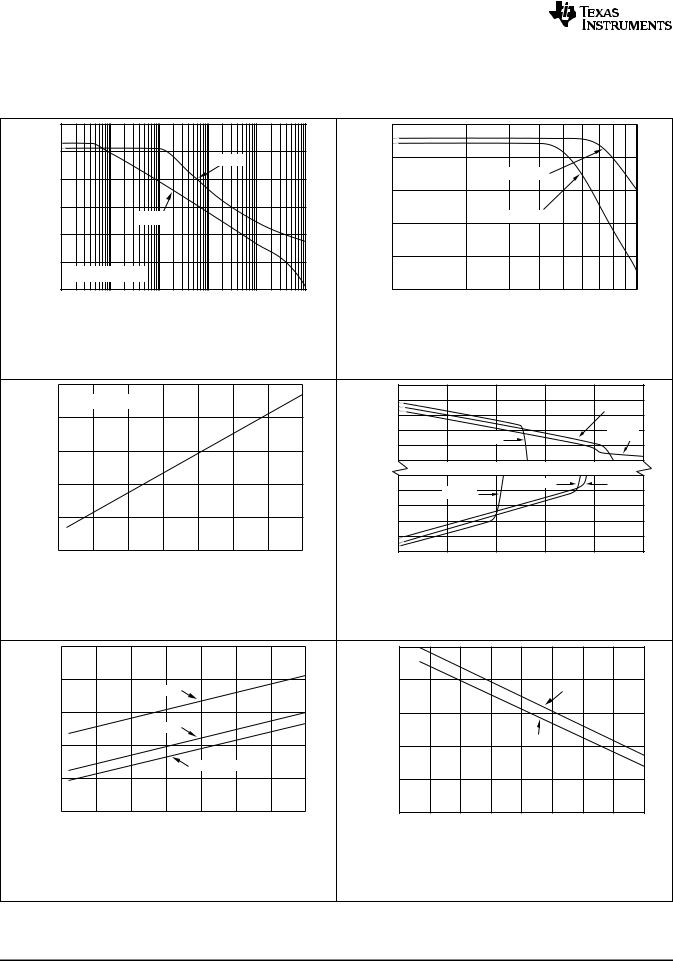
Figure 1. Total Harmonic Distortion + Noise vs Frequency |
Figure 2. Total Harmonic Distortion + Noise vs Frequency |
0.1 |
|
|
|
Single-Ended Mode |
|
0.01 |
|
|
|
|
|
|
|
|
|
|
–VO or +VO Grounded |
|
|
See Figure 3 for Test Circuit |
DIFFERENTIAL MODE |
|
|||||||||||
A: R |
1 |
= 600Ω (250 ft cable) |
|
VO = 10Vrms |
|
|
A: R |
= R |
2 |
= R |
L |
= ∞ (no load) |
V |
O |
= 10Vrms |
|
|
|
|
|
|
|
1 |
|
|
|
|
|
|
||||
B: R1 = ∞ (no cable) |
|
|
|
|
B: R1 = R2 = ∞ RL = 600Ω |
|
|
|
|
|||||||
0.01 |
|
|
|
|
|
<![if ! IE]> <![endif]>(%) |
|
|
|
|
|
|
|
|
|
|
|
|
|
|
|
|
|
|
|
|
|
|
A (no cable) |
|
|||
|
|
|
|
A |
|
<![if ! IE]> <![endif]>THD+N |
|
|
|
|
|
|
|
|||
|
|
|
|
|
0.001 |
|
|
|
|
|
|
|
|
|
||
|
|
|
|
|
|
|
|
|
|
|
|
|
|
|
||
|
|
|
|
|
|
|
|
|
|
|
|
|
|
|
|
|
|
|
|
|
|
B |
|
|
|
|
|
|
|
|
|
|
|
0.001 |
|
|
|
|
|
|
|
|
|
|
|
|
|
|
|
|
|
|
|
|
|
|
|
|
|
|
|
|
|
B (500ft cable) |
|
||
DRV134 Output |
|
|
|
|
INA137 Output |
|
|
|
|
|
||||||
|
|
|
|
|
|
|
|
|
|
|
|
|
|
|||
0.0001 |
|
|
|
|
|
|
0.0001 |
|
|
|
|
|
|
|
|
|
20 |
|
100 |
1k |
10k |
20k |
|
20 |
|
100 |
|
1k |
|
|
10k |
20k |
|
|
|
Frequency (Hz) |
|
|
|
|
|
|
|
|
Frequency (Hz) |
|
|
|
||
Figure 3. Total Harmonic Distortion + Noise |
Figure 4. System Total Harmonic Distortion + Noise |
vs Frequency |
vs Frequency |
6 |
Submit Documentation Feedback |
Copyright © 1998–2014, Texas Instruments Incorporated |
Product Folder Links: DRV134 DRV135

DRV134, DRV135
www.ti.com |
SBOS094B –JANUARY 1998 –REVISED DECEMBER 2014 |
Typical Characteristics (continued)
At TA = 25°C, VS = ±18 V, RL = 600 Ω differential connected between +VO and –VO, unless otherwise noted. |
|
||||||||||||||
|
|
1 |
|
|
|
|
|
|
|
1 |
|
|
|
|
|
|
|
|
f = 1kHz |
|
Single-Ended |
Differential |
|
|
|
DIFFERENTIAL MODE |
|
|
|
||
|
|
|
|
|
Mode |
|
Mode |
|
|
|
|
|
|
|
|
|
|
0.1 |
|
|
|
|
|
|
|
0.1 |
|
|
|
|
|
|
|
|
|
|
500 ft Cable |
500 ft Cable |
|
|
|
|
|
500 ft Cable |
|
||
| <![if ! IE]> <![endif]>THD+N (%) |
|
|
|
RL = 600Ω |
RL = 600Ω |
|
<![if ! IE]> <![endif]>DIM (%) |
|
|
|
RL = 600Ω |
|
|
||
0.01 |
|
|
|
|
|
|
0.01 |
|
|
|
|
|
|||
|
|
|
|
|
|
|
|
|
|
|
|
|
|||
|
|
0.001 |
|
|
|
|
|
|
|
0.001 |
|
|
|
|
|
|
|
|
DRV134 Output |
|
|
No Cable |
|
|
|
BW = 30kHz |
|
|
|
No Cable |
|
|
|
|
|
|
RL = ∞ |
|
|
|
|
|
|
|
RL = ∞ |
||
|
0.0001 |
|
|
|
|
|
|
0.0001 |
|
|
|
|
|||
|
|
|
|
|
|
|
|
|
|
|
|
|
|||
|
|
|
5 |
10 |
15 |
20 |
25 |
30 |
|
5 |
10 |
15 |
20 |
25 |
30 |
|
|
|
|
Output Amplitude (dBu) |
|
|
|
|
Output Amplitude (dBu) |
|
|||||
|
|
Figure 5. Headroom – Total Harmonic Distortion + Noise |
|
|
Figure 6. Dim Intermodulation Distortion |
||||||||||
|
|
|
|
vs Output Amplitude |
|
|
|
|
|
vs Output Amplitude |
|
|
|||
|
|
0.01 |
|
|
|
|
|
|
|
10 |
|
|
|
|
|
|
|
|
DIFFERENTIAL MODE |
|
|
No Cable, RL = ∞ |
|
|
|
|
|
|
|
||
|
|
|
|
|
|
|
|
|
|
|
|
|
|
||
| <![if ! IE]> <![endif]>of Fundamental) |
|
|
|
|
|
|
500 ft Cable, |
|
|
|
|
|
|
|
|
|
|
|
|
|
|
RL = 600Ω |
|
|
5 |
|
|
|
|
|
|
|
|
|
|
|
|
|
|
|
|
|
|
|
|
||
|
0.001 |
|
|
|
|
|
|
<![if ! IE]> <![endif]>Gain (dB) |
|
|
|
|
|
|
|
|
|
2nd Harmonic |
|
|
|
0 |
|
|
|
|
|
||||
|
|
|
|
|
|
|
|
|
|
|
|
|
|||
|
|
|
|
|
|
|
|
|
|
|
|
|
|
||
| <![if ! IE]> <![endif]>Amplitude (% |
|
0.0001 |
|
|
|
|
|
|
<![if ! IE]> <![endif]>Voltage |
|
|
|
|
|
|
|
|
|
|
|
|
|
|
–5 |
|
|
|
|
|
||
|
|
|
|
|
|
|
|
|
|
|
|
|
|
||
|
0.00001 |
|
|
|
|
3rd Harmonic |
|
–10 |
|
|
|
|
|
||
|
|
|
|
|
|
|
|
|
|
|
|
|
|||
|
|
20 |
100 |
|
1k |
10k |
20k |
|
1k |
10k |
100k |
1M |
10M |
||
|
|
|
|
|
Frequency (Hz) |
|
|
|
|
|
Frequency (Hz) |
|
|
||
|
|
Figure 7. Harmonic Distortion Products vs Frequency |
|
|
Figure 8. Gain vs Frequency |
|
|||||||||
|
|
10k |
|
|
|
|
|
|
|
100 |
|
|
|
|
|
|
<![if ! IE]> <![endif]>(nV/√Hz) |
1k |
|
|
|
|
|
|
<![if ! IE]> <![endif]>(µVrms) |
10 |
|
|
|
|
|
|
|
|
|
|
|
|
|
|
|
|
|
|
|
||
|
<![if ! IE]> <![endif]>Noise |
|
|
|
|
|
|
|
<![if ! IE]> <![endif]>Noise |
|
|
|
|
|
|
|
<![if ! IE]> <![endif]>Voltage |
100 |
|
|
|
|
|
|
<![if ! IE]> <![endif]>Voltage |
1 |
|
|
|
|
|
|
|
|
|
|
|
|
|
|
|
|
|
|
|
||
|
|
10 |
|
|
|
|
|
|
|
0.1 |
|
|
|
|
|
|
|
1 |
10 |
100 |
1k |
10k |
100k |
1M |
|
1 |
10 |
100 |
1k |
10k |
100k |
|
|
|
|
|
Frequency (Hz) |
|
|
|
|
|
Frequency (Hz) |
|
|
||
|
|
Figure 9. Output Voltage Noise Spectral Density |
|
|
Figure 10. Output Voltage Noise |
|
|||||||||
|
|
|
|
vs Frequency |
|
|
|
|
|
vs Noise Bandwidth |
|
|
|||
Copyright © 1998–2014, Texas Instruments Incorporated |
Submit Documentation Feedback |
7 |
Product Folder Links: DRV134 DRV135
DRV134, DRV135
SBOS094B –JANUARY 1998 –REVISED DECEMBER 2014 |
www.ti.com |
Typical Characteristics (continued)
At TA = 25°C, VS = ±18 V, RL = 600 Ω differential connected between +VO and –VO, unless otherwise noted. |
|
|
|
|||||||||||||||
|
120 |
|
|
|
|
|
|
|
|
20 |
|
|
|
|
|
|
|
|
| <![if ! IE]> <![endif]>SupplyRejection(dB) |
100 |
|
|
|
+PSRR |
|
|
<![if ! IE]> <![endif]>Voltage Swing (Vrms) |
16 |
|
|
|
|
|
|
|
|
|
|
|
|
|
|
|
|
|
|
|
|
|
|
|
|||||
80 |
|
|
|
|
|
|
|
|
|
|
0.1% Distortion |
|
|
|
|
|||
|
|
|
|
|
|
|
|
|
|
|
|
|
|
|
|
|||
|
|
|
|
|
|
|
|
12 |
|
|
|
|
|
|
|
|
||
60 |
|
|
|
|
|
|
|
|
|
|
0.01% Distortion |
|
|
|
||||
|
|
|
–PSRR |
|
|
|
|
8 |
|
|
|
|
|
|||||
|
|
|
|
|
|
|
|
|
|
|
|
|
|
|
|
|||
40 |
|
|
|
|
|
|
|
|
|
|
|
|
|
|
|
|
||
|
|
|
|
|
|
|
|
|
|
|
|
|
|
|
|
|
||
| <![if ! IE]> <![endif]>Power |
20 |
|
|
|
|
|
|
|
<![if ! IE]> <![endif]>Output |
4 |
|
|
|
|
|
|
|
|
|
|
|
|
|
|
|
RL = 600Ω |
|
|
|
|
|
|
|||||
VS |
= ±4.5V to ±18V |
|
|
|
|
|
|
|
|
|
|
|||||||
|
|
|
|
|
|
Diff Mode |
|
|
|
|
|
|
|
|||||
|
|
|
|
|
|
|
|
|
|
|
|
|
|
|
|
|
||
|
0 |
|
|
|
|
|
|
|
|
0 |
|
|
|
|
|
|
|
|
|
10 |
|
100 |
1k |
10k |
|
100k |
1M |
|
10k |
|
20k |
|
|
50k |
|
80k |
100k |
|
|
|
|
Frequency (Hz) |
|
|
|
|
|
|
|
Frequency (Hz) |
|
|
|
|
||
|
Figure 11. Power Supply Rejection vs Frequency |
|
Figure 12. Maximum Output Voltage Swing vs Frequency |
|||||||||||||||
|
20 |
|
|
|
|
|
|
|
|
18 |
|
|
|
|
|
|
|
|
| <![if ! IE]> <![endif]>OutputVoltage(Vrms) |
THD+N ≤ 0.1% |
|
|
|
|
|
|
16 |
|
|
|
|
|
|
+25°C |
|||
|
|
|
|
|
|
|
|
|
14 |
|
|
|
|
|
|
|||
16 |
|
|
|
|
|
|
|
<![if ! IE]> <![endif]>Voltage Swing (V) |
|
|
|
|
|
|
|
|
||
|
|
|
|
|
|
|
|
|
|
|
|
|
|
|
|
|||
|
|
|
|
|
|
|
|
12 |
|
+125°C |
|
|
|
–55°C |
||||
|
|
|
|
|
|
|
|
|
|
|
|
|
||||||
|
|
|
|
|
|
|
|
10 |
|
|
|
|
|
|
||||
12 |
|
|
|
|
|
|
|
|
|
|
|
|
|
|
|
|||
|
|
|
|
|
|
|
|
|
|
|
|
|
|
|
|
|||
|
|
|
|
|
|
|
|
8 |
|
|
|
|
|
|
|
|
||
|
|
|
|
|
|
|
|
–8 |
|
|
|
|
|
|
|
|
||
8 |
|
|
|
|
|
|
|
–10 |
|
+125°C |
|
+25°C |
|
–55°C |
||||
|
|
|
|
|
|
|
|
|
|
|
|
|
|
|
||||
| <![if ! IE]> <![endif]>Differential |
|
|
|
|
|
|
|
|
<![if ! IE]> <![endif]>Output |
|
|
|
|
|
|
|
|
|
|
|
|
|
|
|
|
|
–12 |
|
|
|
|
|
|
|
|
||
4 |
|
|
|
|
|
|
|
–14 |
|
|
|
|
|
|
|
|
||
|
|
|
|
|
|
|
|
|
|
|
|
|
|
|
|
|||
|
|
|
|
|
|
|
|
–16 |
|
|
|
|
|
|
|
|
||
|
0 |
|
|
|
|
|
|
|
|
–18 |
|
|
|
|
|
|
|
|
|
±4 |
±6 |
±8 |
±10 |
±12 |
±14 |
±16 |
±18 |
|
0 |
|
±20 |
±40 |
±60 |
±80 |
|
±100 |
|
|
|
|
|
Supply Voltage (V) |
|
|
|
|
|
|
|
Output Current (mA) |
|
|
|
|||
|
Figure 13. Output Voltage Swing vs Supply Voltage |
|
Figure 14. Output Voltage Swing vs Output Current |
|||||||||||||||
|
±5.6 |
|
|
|
|
|
|
|
|
±120 |
|
|
|
|
|
|
|
|
| <![if ! IE]> <![endif]>QuiescentCurrent(mA) |
±5.4 |
|
|
|
|
|
|
|
<![if ! IE]> <![endif]>Short-Circuit Current (mA) |
±100 |
|
|
|
|
+ISC |
|
|
|
|
|
|
T = –55°C |
|
|
|
|
|
|
|
|
|
|
|
|
|||
|
|
|
|
|
|
|
|
|
|
|
|
|
|
|
|
|||
±5.2 |
|
|
|
|
|
|
|
±80 |
|
|
|
|
|
|
|
|
||
|
|
|
T = +25°C |
|
|
|
|
|
|
|
|
|
|
|
|
|
||
±5 |
|
|
|
|
|
|
|
±60 |
|
|
|
–ISC |
|
|
|
|
||
|
|
|
|
|
|
|
|
|
|
|
|
|
|
|
||||
|
|
|
|
T = +125°C |
|
|
|
|
|
|
|
|
|
|
|
|||
±4.8 |
|
|
|
|
|
|
|
±40 |
|
|
|
|
|
|
|
|
||
|
|
|
|
|
|
|
|
|
|
|
|
|
|
|
|
|
||
|
±4.6 |
|
|
|
|
|
|
|
|
±20 |
|
|
|
|
|
|
|
|
|
±4 |
±6 |
±8 |
±10 |
±12 |
±14 |
±16 |
±18 |
|
–75 |
–50 |
–25 |
0 |
25 |
50 |
75 |
100 |
125 |
|
|
|
|
Supply Voltage (V) |
|
|
|
|
|
|
|
Temperature ( °C) |
|
|
|
|||
|
Figure 15. Quiescent Current vs Supply Voltage |
|
Figure 16. Short-Circuit Current vs Temperature |
|||||||||||||||
8 |
Submit Documentation Feedback |
Copyright © 1998–2014, Texas Instruments Incorporated |
Product Folder Links: DRV134 DRV135
|
DRV134, DRV135 |
www.ti.com |
SBOS094B –JANUARY 1998 –REVISED DECEMBER 2014 |
Typical Characteristics (continued)
At TA = 25°C, VS = ±18 V, RL = 600 Ω differential connected between +VO and –VO, unless otherwise noted.
<![endif]>Percent of Units (%)
<![if ! IE]><![endif]>50MV/DIV
45 |
|
|
|
|
|
|
|
|
|
|
|
|
|
|
|
|
|
|
|
|
|
35 |
|
|
|
|
|
|
|
|
|
|
|
|
|
|
|
|
|
|
|
|
40 |
|
|
|
|
|
|
|
|
|
|
|
Typical production |
|
|
|
|
|
|
|
|
|
|
|
|
|
|
|
|
Typical production |
|
|
|
||||||||||
|
|
|
|
|
|
|
|
|
|
|
distribution of packaged |
|
|
30 |
|
|
|
|
|
|
|
|
|
|
|
distribution of packaged |
|
|||||||||||||||
|
|
|
|
|
|
|
|
|
|
|
|
|
|
|
|
|
|
|
|
|
|
|
|
|
|
|||||||||||||||||
35 |
|
|
|
|
|
|
|
|
|
|
|
units. All package types |
|
|
|
|
|
|
|
|
|
|
|
|
|
|
units. All package types |
|
||||||||||||||
|
|
|
|
|
|
|
|
|
|
|
included. |
|
|
|
|
|
|
<![if ! IE]> <![endif]>(%) |
|
|
|
|
|
|
|
|
|
|
|
|
included. |
|
|
|
|
|
|
|||||
|
|
|
|
|
|
|
|
|
|
|
|
|
|
|
|
|
|
25 |
|
|
|
|
|
|
|
|
|
|
|
|
|
|
|
|
|
|||||||
30 |
|
|
|
|
|
|
|
|
|
|
|
|
|
|
|
|
|
|
|
|
|
|
|
|
|
|
|
|
|
|
|
|
|
|
|
|
|
|
|
|
||
|
|
|
|
|
|
|
|
|
|
|
|
|
|
|
|
|
|
|
|
|
|
|
|
|
|
|
|
|
|
|
|
|
|
|
|
|
|
|
|
|
||
|
|
|
|
|
|
|
|
|
|
|
|
|
|
|
|
|
|
|
|
<![if ! IE]> <![endif]>Unitsof |
|
|
|
|
|
|
|
|
|
|
|
|
|
|
|
|
|
|
|
|
|
|
25 |
|
|
|
|
|
|
|
|
|
|
|
|
|
|
|
|
|
|
|
|
20 |
|
|
|
|
|
|
|
|
|
|
|
|
|
|
|
|
|
|
|
|
|
|
|
|
|
|
|
|
|
|
|
|
|
|
|
|
|
|
|
|
|
|
|
|
|
|
|
|
|
|
|
|
|
|
|
|
|
|
|
|
|
|
||
|
|
|
|
|
|
|
|
|
|
|
|
|
|
|
|
|
|
|
|
|
|
|
|
|
|
|
|
|
|
|
|
|
|
|
|
|
|
|
|
|
|
|
20 |
|
|
|
|
|
|
|
|
|
|
|
|
|
|
|
|
|
|
|
|
<![if ! IE]> <![endif]>Percent |
15 |
|
|
|
|
|
|
|
|
|
|
|
|
|
|
|
|
|
|
|
|
|
|
|
|
|
|
|
|
|
|
|
|
|
|
|
|
|
|
|
|
|
|
|
|
|
|
|
|
|
|
|
|
|
|
|
|
|
|
|
|
|
||
15 |
|
|
|
|
|
|
|
|
|
|
|
|
|
|
|
|
|
|
|
|
10 |
|
|
|
|
|
|
|
|
|
|
|
|
|
|
|
|
|
|
|
|
|
|
|
|
|
|
|
|
|
|
|
|
|
|
|
|
|
|
|
|
|
|
|
|
|
|
|
|
|
|
|
|
|
|
|
|
|
|
|
|
|
|
||
|
|
|
|
|
|
|
|
|
|
|
|
|
|
|
|
|
|
|
|
|
|
|
|
|
|
|
|
|
|
|
|
|
|
|
|
|
|
|
|
|
|
|
10 |
|
|
|
|
|
|
|
|
|
|
|
|
|
|
|
|
|
|
|
|
|
|
|
|
|
|
|
|
|
|
|
|
|
|
|
|
|
|
|
|
|
|
5 |
|
|
|
|
|
|
|
|
|
|
|
|
|
|
|
|
|
|
|
|
|
5 |
|
|
|
|
|
|
|
|
|
|
|
|
|
|
|
|
|
|
|
|
|
|
|
|
|
|
|
|
|
|
|
|
|
|
|
|
|
|
|
|
|
|
|
|
|
|
|
|
|
|
|
|
|
|
|
|
|
|
|
|
|
|
|
0 |
|
|
|
|
|
|
|
|
|
|
|
|
|
|
|
|
|
|
|
|
|
0 |
|
|
|
|
|
|
|
|
|
|
|
|
|
|
|
|
|
|
|
|
| <![if ! IE]> <![endif]>10 |
<![if ! IE]> <![endif]>–9 |
<![if ! IE]> <![endif]>–8 |
<![if ! IE]> <![endif]>–7 |
<![if ! IE]> <![endif]>–6 |
<![if ! IE]> <![endif]>–5 |
<![if ! IE]> <![endif]>–4 |
<![if ! IE]> <![endif]>–3 |
<![if ! IE]> <![endif]>–2 |
<![if ! IE]> <![endif]>–1 |
<![if ! IE]> <![endif]>0 |
<![if ! IE]> <![endif]>1 |
<![if ! IE]> <![endif]>2 |
<![if ! IE]> <![endif]>3 |
<![if ! IE]> <![endif]>4 |
<![if ! IE]> <![endif]>5 |
<![if ! IE]> <![endif]>6 |
<![if ! IE]> <![endif]>7 |
<![if ! IE]> <![endif]>8 |
<![if ! IE]> <![endif]>9 |
<![if ! IE]> <![endif]>10 |
|
<![if ! IE]> <![endif]>–250 |
<![if ! IE]> <![endif]>–225 |
<![if ! IE]> <![endif]>–200 |
<![if ! IE]> <![endif]>–175 |
<![if ! IE]> <![endif]>–150 |
<![if ! IE]> <![endif]>–125 |
<![if ! IE]> <![endif]>–100 |
<![if ! IE]> <![endif]>–75 |
<![if ! IE]> <![endif]>–50 |
<![if ! IE]> <![endif]>–25 |
<![if ! IE]> <![endif]>0 |
<![if ! IE]> <![endif]>25 |
<![if ! IE]> <![endif]>50 |
<![if ! IE]> <![endif]>75 |
<![if ! IE]> <![endif]>100 |
<![if ! IE]> <![endif]>125 |
<![if ! IE]> <![endif]>150 |
<![if ! IE]> <![endif]>175 |
<![if ! IE]> <![endif]>200 |
<![if ! IE]> <![endif]>225 |
<![if ! IE]> <![endif]>250 |
| <![if ! IE]> <![endif]>– |
|
|||||||||||||||||||||||||||||||||||||||||
Differential Offset Voltage (mV)
Common-Mode Offset Voltage (mV)
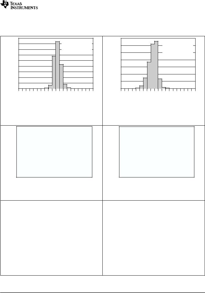
Figure 17. Differential Offset Voltage |
Figure 18. Common-Mode Offset Voltage |
|
Production Distribution |
||
Production Distribution |
||
|
<![endif]>50MV/DIV
2µS/DIV |
2µS/DIV |
CL = 100 pF |
CL = 1000 pF |
Figure 19. Small-Signal Step Response |
Figure 20. Small-Signal Step Response |
| <![if ! IE]> <![endif]>5V/DIV |
|
<![if ! IE]> <![endif]>5V/DIV |
|
|
|
|
|
2µS/DIV |
2µS/DIV |
CL = 100 pF |
CL = 1000 pF |
Figure 21. Large-Signal Step Response |
Figure 22. Large-Signal Step Response |
Copyright © 1998–2014, Texas Instruments Incorporated |
Submit Documentation Feedback |
9 |
Product Folder Links: DRV134 DRV135
DRV134, DRV135
SBOS094B –JANUARY 1998 –REVISED DECEMBER 2014 |
www.ti.com |
Typical Characteristics (continued)
At TA = 25°C, VS = ±18 V, RL = 600 Ω differential connected between +VO and –VO, unless otherwise noted.
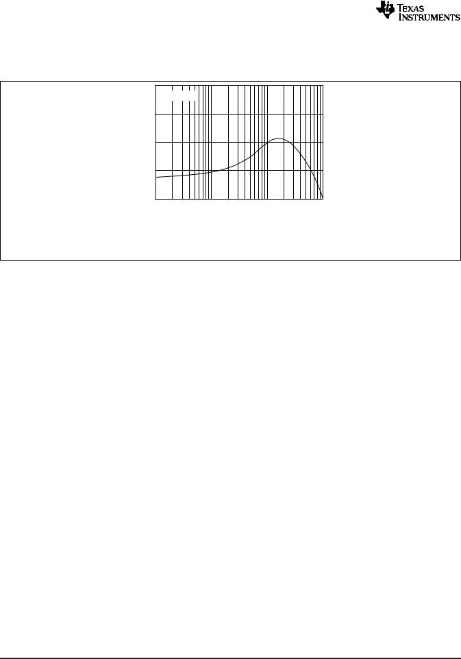
<![endif]>Overshoot (%)
40
100mV Step
30
20
10
0
10 |
100 |
1k |
10k |
Load Capacitance (pF)
Figure 23. Small-Signal Step Overshoot vs Load Capacitance
10 |
Submit Documentation Feedback |
Copyright © 1998–2014, Texas Instruments Incorporated |
Product Folder Links: DRV134 DRV135
Loading...