


DAC7552
Actual Size |
DAC7552 |
3 mm x 3 mm |
|
www.ti.com |
SLAS442B –JANUARY 2005 –REVISED JUNE 2005 |
|
12-BIT, DUAL, ULTRALOW GLITCH, VOLTAGE OUTPUT
DIGITAL-TO-ANALOG CONVERTER
FEATURES
∙2.7-V to 5.5-V Single Supply
∙12-Bit Linearity and Monotonicity
∙Rail-to-Rail Voltage Output
∙Settling Time: 5 µs (Max)
∙Ultralow Glitch Energy: 0.1 nVs
∙Ultralow Crosstalk: –100 dB
∙Low Power: 440 µA (Max)
∙Per-Channel Power Down: 2 µA (Max)
∙Power-On Reset to Zero Scale
∙SPI-Compatible Serial Interface: Up to 50 MHz
∙Daisy-Chain Capability
∙Asynchronous Hardware Clear
∙Simultaneous or Sequential Update
∙Specified Temperature Range: –40°C to 105°C
∙Small 3-mm × 3-mm, 16-Lead QFN Package
APPLICATIONS
∙Portable Battery-Powered Instruments
∙Digital Gain and Offset Adjustment
∙Programmable Voltage and Current Sources
∙Programmable Attenuators
∙Industrial Process Control
DESCRIPTION
The DAC7552 is a 12-bit, dual-channel, volt- age-output DAC with exceptional linearity and monotonicity. Its proprietary architecture minimizes undesired transients such as code-to-code glitch and channel-to-channel crosstalk. The low-power DAC7552 operates from a single 2.7-V to 5.5-V supply. The DAC7552 output amplifiers can drive a 2-kΩ, 200-pF load rail-to-rail with 5-µs settling time; the output range is set using an external voltage reference.
The 3-wire serial interface operates at clock rates up to 50 MHz and is compatible with SPI, QSPI, Microwire™, and DSP interface standards. The outputs of all DACs may be updated simultaneously or sequentially. The parts incorporate a power-on-reset circuit to ensure that the DAC outputs power up to zero volts and remain there until a valid write cycle to the device takes place. The parts contain a power-down feature that reduces the current consumption of the device to under 2 µA.
The small size and low-power operation makes the DAC7552 ideally suited for battery-operated portable applications. The power consumption is typically 1.5 mW at 5 V, 0.75 mW at 3 V, and reduces to 1 µW in power-down mode.
The DAC7552 is available in a 16-lead QFN package and is specified over –40°C to 105°C.
FUNCTIONAL BLOCK DIAGRAM
VDD |
IOVDD |
VREFA |
SCLK |
|
|
Input |
DAC |
|
|
Register |
Register |
|
|
Interface |
|
|
|
SYNC |
Logic |
|
|
|
|
|
|
Input |
DAC |
SDIN |
|
|
Register |
Register |
|
|
|
|
|
SDO |
|
DAC7552 |
Power-On |
|
|
|
Reset |
||
DCEN |
CLR |
|
GND |
|
|
_ |
VFBA |
|
|
|
String |
+ |
VOUT A |
DAC A |
|
|
|
_ |
VFBB |
|
VOUT B |
|
String |
+ |
|
DAC B |
|
|
|
Power-Down |
|
|
Logic |
|
VREFB |
PD |
|
Please be aware that an important notice concerning availability, standard warranty, and use in critical applications of Texas Instruments semiconductor products and disclaimers thereto appears at the end of this data sheet.
Microwire is a trademark of National Semiconductor Corporation.
PRODUCTION DATA information is current as of publication date. |
Copyright © 2005, Texas Instruments Incorporated |
Products conform to specifications per the terms of the Texas |
|
Instruments standard warranty. Production processing does not |
|
necessarily include testing of all parameters. |
|
DAC7552
www.ti.com
SLAS442B –JANUARY 2005 –REVISED JUNE 2005
This integrated circuit can be damaged by ESD. Texas Instruments recommends that all integrated circuits be handled with appropriate precautions. Failure to observe proper handling and installation procedures can cause damage.
ESD damage can range from subtle performance degradation to complete device failure. Precision integrated circuits may be more susceptible to damage because very small parametric changes could cause the device not to meet its published specifications.
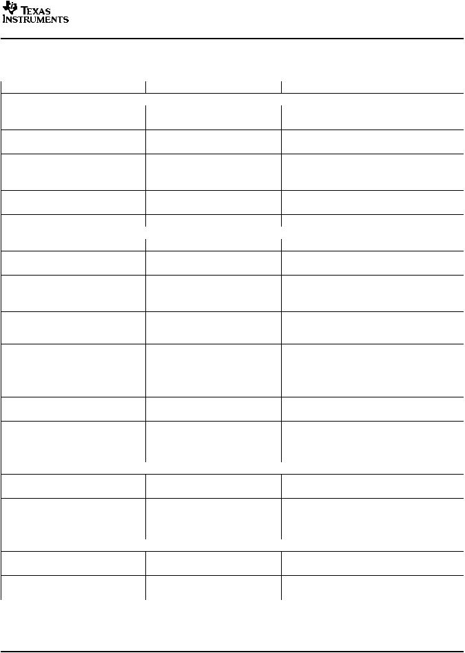
ORDERING INFORMATION(1)
|
|
PACKAGE |
SPECIFIED |
PACKAGE |
ORDERING |
TRANSPORT |
|
PRODUCT |
PACKAGE |
TEMPERATURE |
|||||
DESIGNATOR |
MARKING |
NUMBER |
MEDIA |
||||
|
|
RANGE |
|||||
|
|
|
|
|
|
||
DAC7552 |
16 QFN |
RGT |
–40°C TO 105°C |
D752 |
DAC7552IRGTT |
250-piece Tape and Reel |
|
DAC7552IRGTR |
3000-piece Tape and Reel |
||||||
|
|
|
|
|
(1)For the most current package and ordering information, see the Package Option Addendum at the end of this document, or see the TI Web site at www.ti.com.
ABSOLUTE MAXIMUM RATINGS
over operating free-air temperature range (unless otherwise noted)(1)
|
UNIT |
VDD to GND |
–0.3 V to 6 V |
Digital input voltage to GND |
–0.3 V to VDD + 0.3 V |
VOUT to GND |
–0.3 V to VDD+ 0.3 V |
Operating temperature range |
–40°C to 105°C |
Storage temperature range |
–65°C to 150°C |
Junction temperature (TJ Max) |
150°C |
(1)Stresses above those listed under “AbsoluteMaximum Ratings” may cause permanent damage to the device. Exposure to absolute maximum conditions for extended periods may affect device reliability.
2
DAC7552
www.ti.com
SLAS442B –JANUARY 2005 –REVISED JUNE 2005
ELECTRICAL CHARACTERISTICS
VDD = 2.7 V to 5.5 V, VREF = VDD, RL = 2 kΩ to GND; CL = 200 pF to GND; all specifications –40°C to 105°C, unless otherwise specified
PARAMETER |
TEST CONDITIONS |
MIN |
TYP |
MAX |
UNITS |
STATIC PERFORMANCE(1) |
|
|
|
|
|
Resolution |
|
|
12 |
|
Bits |
Relative accuracy |
|
|
±0.35 |
±1 |
LSB |
Differential nonlinearity |
Specified monotonic by design |
|
±0.08 |
±0.5 |
LSB |
Offset error |
|
|
|
±12 |
mV |
Zero-scale error |
All zeroes loaded to DAC register |
|
|
±12 |
mV |
Gain error |
|
|
|
±0.15 |
%FSR |
Full-scale error |
|
|
|
±0.5 |
%FSR |
Zero-scale error drift |
|
|
7 |
|
µV/°C |
Gain temperature coefficient |
|
|
3 |
|
ppm of FSR/°C |
PSRR |
VDD = 5 V |
|
0.75 |
|
mV/V |
OUTPUT CHARACTERISTICS(2) |
|
|
|
|
|
Output voltage range |
|
0 |
|
VREF |
V |
Output voltage settling time |
RL = 2 kW; 0 pF < CL < 200 pF |
|
|
5 |
µs |
Slew rate |
|
|
1.8 |
|
V/µs |
Capacitive load stability |
RL = ¥ |
|
470 |
|
pF |
|
RL = 2 kW |
|
1000 |
|
|
|
|
|
|
||
Digital-to-analog glitch impulse |
1 LSB change around major carry |
|
0.1 |
|
nV-s |
Channel-to-channel crosstalk |
1-kHz full-scale sine wave, |
|
–100 |
|
dB |
|
outputs unloaded |
|
|
|
|
Digital feedthrough |
|
|
0.1 |
|
nV-s |
Output noise density (10-kHz offset fre- |
|
|
120 |
|
nV/rtHz |
quency) |
|
|
|
|
|
Total harmonic distortion |
FOUT = 1 kHz, FS = 1 MSPS, |
|
–85 |
|
dB |
|
BW = 20 kHz |
|
|
|
|
DC output impedance |
|
|
1 |
|
W |
Short-circuit current |
VDD = 5 V |
|
50 |
|
mA |
|
VDD = 3 V |
|
20 |
|
|
|
|
|
|
||
Power-up time |
Coming out of power-down mode, |
|
15 |
|
|
|
VDD = 5 V |
|
|
|
µs |
|
Coming out of power-down mode, |
|
15 |
|
|
|
|
|
|
||
|
VDD = 3 V |
|
|
|
|
REFERENCE INPUT |
|
|
|
|
|
VREF Input range |
|
0 |
|
VDD |
V |
Reference input impedance |
VREFA and VREFB shorted together |
|
50 |
|
kW |
|
VREFA = VREFB = VDD = 5 V, |
|
100 |
250 |
|
Reference current |
VREFA and VREFB shorted together |
|
|
|
µA |
VREFA = VREFB = VDD = 3 V, |
|
60 |
123 |
||
|
|
|
|||
|
VREFA and VREFB shorted together |
|
|
|
|
LOGIC INPUTS(2) |
|
|
|
|
|
Input current |
|
|
|
±1 |
µA |
VIN_L, Input low voltage |
IOVDD ³ 2.7 V |
|
|
0.3 IOVDD |
V |
VIN_H, Input high voltage |
IOVDD ³ 2.7 V |
0.7 IOVDD |
|
|
V |
Pin capacitance |
|
|
|
3 |
pF |
(1)Linearity tested using a reduced code range of 30 to 4065; output unloaded.
(2)Specified by design and characterization, not production tested. For 1.8 V < IOVDD < 2.7 V, It is recommended that VIH = IOVDD, VIL = GND.
3
DAC7552
www.ti.com
SLAS442B –JANUARY 2005 –REVISED JUNE 2005
ELECTRICAL CHARACTERISTICS (continued)
VDD = 2.7 V to 5.5 V, VREF = VDD, RL = 2 kΩ to GND; CL = 200 pF to GND; all specifications –40°C to 105°C, unless otherwise specified
PARAMETER |
TEST CONDITIONS |
MIN |
TYP |
MAX |
UNITS |
 POWER REQUIREMENTS
VDD,, IOVDD (3)
 IDD(normal operation)
VDD = 3.6 V to 5.5 V
VDD = 2.7 V to 3.6 V
 IDD (all power-down modes)
VDD = 3.6 V to 5.5 V
VDD = 2.7 V to 3.6 V
 POWER EFFICIENCY
IOUT/IDD
|
2.7 |
5.5 |
V |
|
DAC active and excluding load current |
|
|
|
|
VIH = IOVDD and VIL = GND |
300 |
440 |
µA |
|
250 |
400 |
|||
|
|
|||
VIH = IOVDD and VIL = GND |
0.2 |
2 |
µA |
|
0.05 |
2 |
|||
|
|
|||
ILOAD = 2 mA, VDD = 5 V |
93% |
|
|
(3)IOVDD operates down to 1.8 V with slightly degraded timing, as long as VIH = IOVDD and VIL = GND.
4

DAC7552
www.ti.com
SLAS442B –JANUARY 2005 –REVISED JUNE 2005
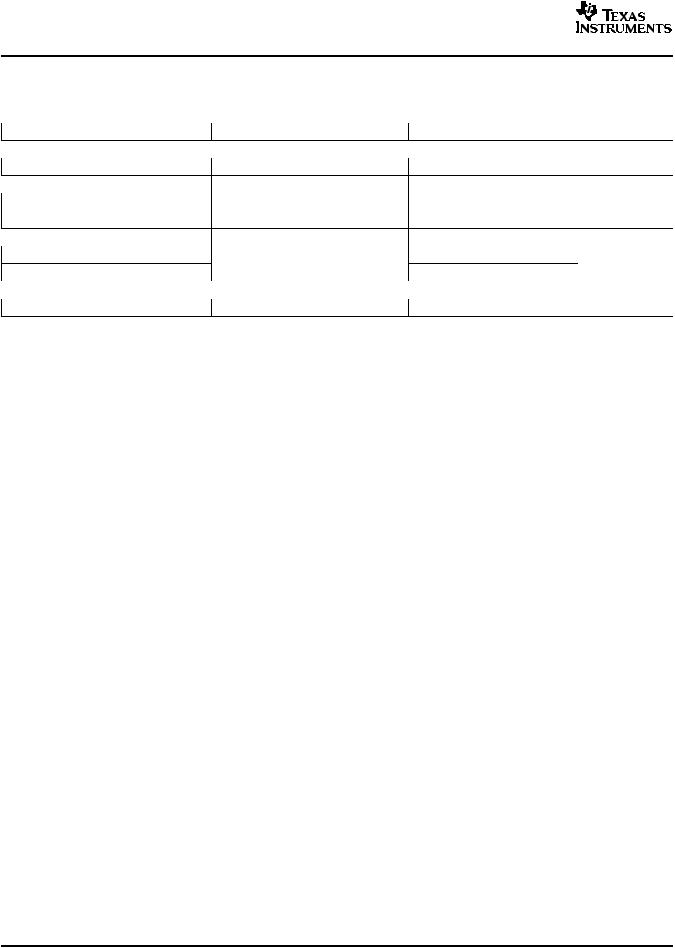
TIMING CHARACTERISTICS(1) (2)
VDD = 2.7 V to 5.5 V, RL = 2 kΩ to GND; all specifications –40°C to 105°C, unless otherwise specified
|
PARAMETER |
t (3) |
SCLK cycle time |
1 |
|
t2 |
SCLK HIGH time |
t3 |
SCLK LOW time |
t4 |
SYNC falling edge to SCLK falling edge setup |
time |
|
t5 |
Data setup time |
t6 |
Data hold time |
t7 |
SCLK falling edge to SYNC rising edge |
t8 |
Minimum SYNC HIGH time |
t9 |
SCLK falling edge to SDO valid |
t10 |
CLR pulse width low |
TEST CONDITIONS |
MIN |
TYP |
MAX UNITS |
VDD = 2.7 V to 3.6 V |
20 |
|
ns |
VDD = 3.6 V to 5.5 V |
20 |
|
|
|
|
||
VDD = 2.7 V to 3.6 V |
10 |
|
ns |
VDD = 3.6 V to 5.5 V |
10 |
|
|
|
|
||
VDD = 2.7 V to 3.6 V |
10 |
|
ns |
VDD = 3.6 V to 5.5 V |
10 |
|
|
|
|
||
VDD = 2.7 V to 3.6 V |
4 |
|
ns |
VDD = 3.6 V to 5.5 V |
4 |
|
|
|
|
||
VDD = 2.7 V to 3.6 V |
5 |
|
ns |
VDD = 3.6 V to 5.5 V |
5 |
|
|
|
|
||
VDD = 2.7 V to 3.6 V |
4.5 |
|
ns |
VDD = 3.6 V to 5.5 V |
4.5 |
|
|
|
|
||
VDD = 2.7 V to 3.6 V |
0 |
|
ns |
VDD = 3.6 V to 5.5 V |
0 |
|
|
|
|
||
VDD = 2.7 V to 3.6 V |
20 |
|
ns |
VDD = 3.6 V to 5.5 V |
20 |
|
|
|
|
||
VDD = 2.7 V to 3.6 V |
10 |
|
ns |
VDD = 3.6 V to 5.5 V |
10 |
|
|
|
|
||
VDD = 2.7 V to 3.6 V |
10 |
|
ns |
VDD = 3.6 V to 5.5 V |
10 |
|
|
|
|
(1)All input signals are specified with tR = tF = 1 ns (10% to 90% of VDD) and timed from a voltage level of (VIL + VIH)/2.
(2)See Serial Write Operation timing diagram Figure 1.
(3)Maximum SCLK frequency is 50 MHz at VDD = 2.7 V to 5.5 V.
|
|
|
|
t1 |
|
|
|
|
|
|
SCLK |
|
|
|
|
|
|
|
|
|
|
|
t8 |
|
t |
t2 |
|
|
t |
|
|
|
|
|
t4 |
3 |
|
|
|
|
|
|
|
|
|
|
|
|
|
7 |
|
|
|
|
SYNC |
|
|
|
|
|
|
|
|
|
|
|
t5 |
|
t6 |
|
|
|
|
|
|
|
SDIN |
D15 |
D14 |
D13 |
D12 |
D11 |
D1 |
D0 |
D15 |
|
D0 |
|
|
|
|
Input Word n |
|
|
t9 |
Input Word n+1 |
|
|
|
|
|
|
|
|
|
|
|
|
|
SDO |
|
|
|
|
|
|
|
D15 |
D14 |
D0 |
|
|
|
|
Undefined |
|
|
|
Input Word n |
|
|
CLR |
|
t10 |
|
|
|
|
|
|
|
|
|
|
|
|
|
|
|
|
|
|
|
Figure 1. Serial Write Operation
5
DAC7552
www.ti.com
SLAS442B –JANUARY 2005 –REVISED JUNE 2005
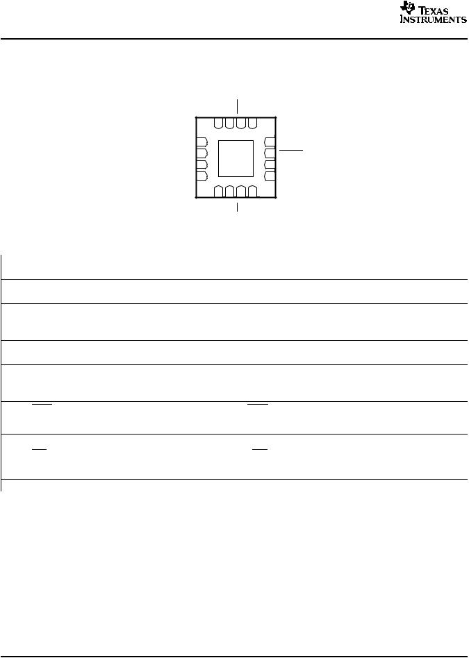
PIN DESCRIPTION |
|
||||
|
RGT PACKAGE |
|
|||
|
(TOP VIEW) |
|
|||
|
VFBA |
VREFA |
CLR |
SDIN |
|
|
16 |
15 |
14 |
13 |
|
VOUTA |
1 |
|
|
12 |
SCLK |
VDD |
2 |
|
|
11 |
SYNC |
GND |
3 |
|
|
10 |
IOVDD |
VOUTB |
4 |
6 |
7 |
9 |
SDO |
|
5 |
8 |
|
||
|
VFBB |
VREFB |
PD |
DCEN |
|
|
|
Terminal Functions |
TERMINAL |
DESCRIPTION |
|
NO. |
NAME |
|
1 |
VOUTA |
Analog output voltage from DAC A |
2 |
VDD |
Analog voltage supply input |
3 |
GND |
Ground |
4 |
VOUTB |
Analog output voltage from DAC B |
5 |
VFBB |
DAC B amplifier sense input. (For voltage output operation, connect to VOUTB externally.) |
6 |
VREFB |
Positive reference voltage input for DAC B |
7 |
PD |
Power-down |
8 |
DCEN |
Daisy-chain enable |
9 |
SDO |
Serial data output |
10 |
IOVDD |
I/O voltage supply input. (For single supply operation, connect to VDD externally.) |
11 |
SYNC |
Frame synchronization input. The falling edge of the SYNC pulse indicates the start of a serial data frame shifted out |
|
|
to the DAC7552 |
12 |
SCLK |
Serial clock input |
13 |
SDIN |
Serial data input |
14 |
CLR |
Asynchronous input to clear the DAC registers. When CLR is low, the DAC registers are set to 000H and the output |
|
|
voltage to 0 V. |
15 |
VREFA |
Positive reference voltage input for DAC A |
16 |
VFBA |
DAC A amplifier sense input. (For voltage output operation, connect to VOUTA externally.) |
6
DAC7552
www.ti.com
|
SLAS442B –JANUARY 2005 –REVISED JUNE 2005 |
TYPICAL CHARACTERISTICS |
|
LINEARITY ERROR AND |
LINEARITY ERROR AND |
DIFFERENTIAL LINEARITY ERROR |
DIFFERENTIAL LINEARITY ERROR |
vs |
vs |
DIGITAL INPUT CODE |
DIGITAL INPUT CODE |
|
1 |
|
|
|
|
|
|
|
|
|
1 |
|
− LSB |
|
Channel A |
|
VREF = 4.096 V |
|
|
VDD = 5 V |
|
− LSB |
|
||
0.5 |
|
|
|
|
|
|
|
|
0.5 |
|||
Error |
0 |
|
|
|
|
|
|
|
|
Error |
0 |
|
Linearity |
|
|
|
|
|
|
|
|
Linearity |
|||
−0.5 |
|
|
|
|
|
|
|
|
−0.5 |
|||
|
|
|
|
|
|
|
|
|
|
|||
|
−1 |
|
|
|
|
|
|
|
|
|
−1 |
|
− LSB |
|
|
|
|
|
|
|
|
|
− LSB |
||
0.5 |
|
|
|
|
|
|
|
|
0.5 |
|||
|
|
|
|
|
|
|
|
|
|
|||
Error |
0.25 |
|
|
|
|
|
|
|
|
Error |
0.25 |
|
|
|
|
|
|
|
|
|
|
|
|||
Linearity |
0 |
|
|
|
|
|
|
|
|
Linearity |
0 |
|
|
|
|
|
|
|
|
|
|
||||
−0.25 |
|
|
|
|
|
|
|
|
|
|||
Differential |
|
|
|
|
|
|
|
|
Differential |
−0.25 |
||
|
|
|
|
|
|
|
|
|
||||
−0.5 |
|
|
|
|
|
|
|
|
−0.5 |
|||
0 |
512 |
1024 |
1536 |
2048 |
2560 |
3072 |
3584 |
4096 |
||||
|
||||||||||||
|
|
|
|
|
|
|
|
|
|
|||
Digital Input Code
Channel B |
VREF = 4.096 V |
VDD = 5 V |
0 |
512 |
1024 |
1536 |
2048 |
2560 |
3072 |
3584 |
4096 |
Digital Input Code
|
|
|
|
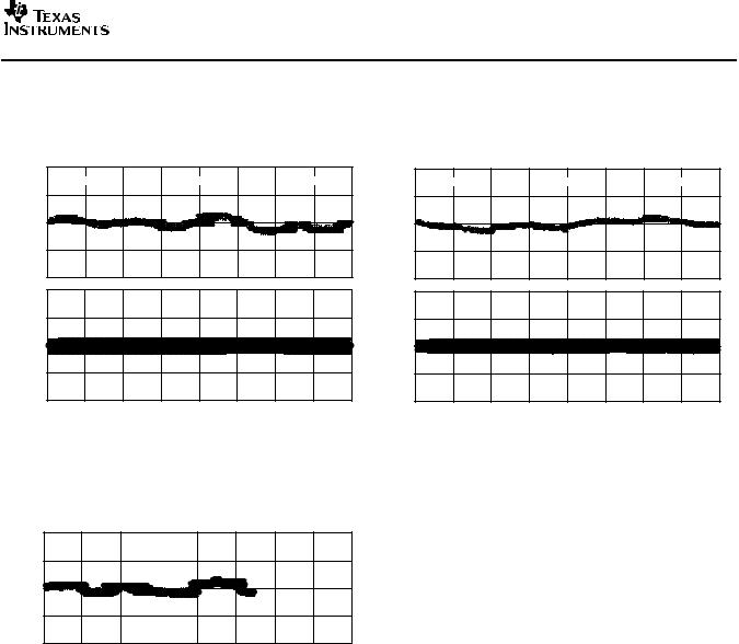
|
Figure 2. |
|
|
|
|
|
|
|
|
LINEARITY ERROR AND |
|
|
|||
|
|
|
DIFFERENTIAL LINEARITY ERROR |
|
|||||
|
|
|
|
|
vs |
|
|
|
|
|
|
|
|
DIGITAL INPUT CODE |
|
|
|
||
LSB− |
1 |
|
|
|
|
|
|
|
|
0.5 |
Channel A |
|
|
VREF = 2.5 V |
|
|
VDD = 2.7 V |
|
|
|
|
|
|
|
|
|
|||
Error |
0 |
|
|
|
|
|
|
|
|
Linearity |
|
|
|
|
|
|
|
|
|
−0.5 |
|
|
|
|
|
|
|
|
|
LSB− |
−1 |
|
|
|
|
|
|
|
|
0.5 |
|
|
|
|
|
|
|
|
|
|
|
|
|
|
|
|
|
|
|
Error |
0.25 |
|
|
|
|
|
|
|
|
Linearity |
0 |
|
|
|
|
|
|
|
|
Differential |
|
|
|
|
|
|
|
|
|
0 |
512 |
1024 |
1536 |
2048 |
2560 |
3072 |
3584 |
4096 |
|
|
−0.25 |
|
|
|
|
|
|
|
|
|
−0.5 |
|
|
|
|
|
|
|
|
|
|
|
|
Digital Input Code |
|
|
|
||
Figure 3.
LINEARITY ERROR AND
DIFFERENTIAL LINEARITY ERROR vs
DIGITAL INPUT CODE
LSB |
1 |
|
|
|
|
|
|
|
|
|
Channel B |
|
|
VREF = 2.5 V |
|
|
VDD = 2.7 V |
|
|
|
|
|
|
|
|
|
|||
Error − |
0.5 |
|
|
|
|
|
|
|
|
0 |
|
|
|
|
|
|
|
|
|
Linearity |
|
|
|
|
|
|
|
|
|
−0.5 |
|
|
|
|
|
|
|
|
|
|
|
|
|
|
|
|
|
|
|
LSB− |
−1 |
|
|
|
|
|
|
|
|
0.5 |
|
|
|
|
|
|
|
|
|
|
|
|
|
|
|
|
|
|
|
Error |
0.25 |
|
|
|
|
|
|
|
|
Linearity |
0 |
|
|
|
|
|
|
|
|
Differential |
−0.25 |
|
|
|
|
|
|
|
|
0 |
512 |
1024 |
1536 |
2048 |
2560 |
3072 |
3584 |
4096 |
|
|
−0.5 |
|
|
|
|
|
|
|
|
Digital Input Code
Figure 4. |
Figure 5. |
7
 Loading...