


Texas Instruments CY74FCT823ATSOC, CY74FCT823ATQCT, CY74FCT823ATQC, CY74FCT823ATPC, CY74FCT821CTSOCT Datasheet
...
Data sheet acquired from Cypress Semiconductor Corporation. Data sheet modified to remove devices not offered.
CY74FCT821T
CY74FCT823T
CY74FCT825T
SCCS033 - May 1994 - Revised March 2000
8-/9-/10-Bit Bus Interface Registers
Features |
Functional Description |
•Function, pinout, and drive compatible with FCT, F, and Am29821/23/25 logic
•FCT-C speed at 6.0 ns max.
FCT-B speed at 7.5 ns max.
• Reduced V (typically = 3.3V) versions of equivalent
OH
FCT functions
•Edge-rate control circuitry for significantly improved noise characteristics
•Power-off disable feature
•Matched rise and fall times
•Fully compatible with TTL input and output logic levels
•ESD > 2000V
• Sink current |
64 mA |
Source current |
32 mA |
•High-speed parallel registers with positive edge-triggered D-type flip-flops
•Buffered common clock enable (EN) and asynchronous clear input (CLR)
•Extended commercial range of−40˚C to +85˚C
These bus interface registers are designed to eliminate the extra packages required to buffer existing registers and provide extra data width for wider address/data paths or buses carrying parity. The FCT821T is a buffered, 10-bit wide version of the popular FCT374 function. The FCT823T is a 9-bit wide buffered register with clock enable (EN) and clear (CLR) ideal for parity bus interfacing in high-performance microprogrammed systems. The FCT825T is an 8-bit buffered register with all the FCT823T controls plus multiple enables (OE1,
OE2, OE3) to allow multiuser control of the interface, e.g., CS, DMA, and RD/WR. They are ideal for use as an output port requiring high IOL/IOH.
These devices are designed for high-capacitance load drive capability, while providing low-capacitance bus loading at both inputs and outputs. Outputs are designed for low-capacitance bus loading in the high-impedance state and are designed with a power-off disable feature to allow for live insertion of boards.
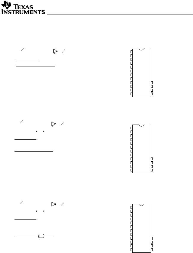
Logic Block Diagram |
|
|
|
|
|
|
|
|
|
D0 |
D1 |
D2 |
D3 |
|
D4 |
D5 |
DN- 1 |
DN |
|
EN[1] |
|
|
|
|
|
|
|
|
|
CLR [1] |
|
|
|
|
|
|
|
|
|
CL |
|
CL |
CL |
CL |
CL |
|
CL |
CL |
CL |
D Q |
|
D Q |
D Q |
D Q |
D Q |
|
D Q |
D Q |
D Q |
CP |
|
CP |
CP |
CP |
CP |
|
CP |
CP |
CP |
Q |
|
Q |
Q |
Q |
Q |
|
Q |
Q |
Q |
CP |
|
|
|
|
|
|
|
|
|
OE |
|
|
|
|
|
|
|
|
|
|
Y0 |
Y1 |
Y2 |
|
Y3 |
Y4 |
Y5 |
Yn- 1 |
Yn |
Note:
1.Not on FCT821.
Copyright © 2000, Texas Instruments Incorporated
CY74FCT821T
CY74FCT823T
CY74FCT825T
Logic Diagrams |
Pin Configurations |
FCT821T (10-Bit Register)
DIP/QSOP/SOIC
Top View
D |
10 |
D |
|
|
10 |
|
|
|
|
1 |
|
|
|
|
||||
|
|
|
|
|
|
|
|
|
|
|
||||||||
|
|
|
|
|
|
|
|
|||||||||||
|
|
|
|
|
Q |
|
|
Y |
|
OE |
|
|
24 |
|
VCC |
|||
|
|
|
CP |
|
|
|
|
D0 |
2 |
|
23 |
|
Y0 |
|||||
|
|
|
|
|
|
3 |
|
|
||||||||||
CP |
|
|
|
|
|
|
|
|
|
|
D1 |
|
22 |
|
Y1 |
|||
|
|
|
|
|
|
|
|
|
|
|
|
D2 |
4 |
|
21 |
|
Y2 |
|
|
|
|
|
|
|
|
|
|
|
|
|
|||||||
OE |
|
|
|
|
|
|
|
|
|
|
|
D3 |
5 FCT821T |
20 |
|
Y3 |
||
|
|
|
|
|
|
|
|
|
|
|
|
|||||||
|
|
|
|
|
|
|
|
|
|
|
|
|
||||||
|
|
|
|
|
|
|
|
|
|
|
|
D4 |
|
|
||||
|
|
|
|
|
|
|
|
|
|
|
|
6 |
|
19 |
|
Y4 |
||
|
|
|
|
|
|
|
|
|
|
|
|
D5 |
7 |
|
18 |
|
Y5 |
|
|
|
|
|
|
|
|
|
|
|
|
|
|
||||||
|
|
|
|
|
|
|
|
|
|
|
|
D6 |
8 |
|
17 |
|
Y6 |
|
|
|
|
|
|
|
|
|
|
|
|
|
|
||||||
|
|
|
|
|
|
|
|
|
|
|
|
D7 |
9 |
|
16 |
|
Y7 |
|
|
|
|
|
|
|
|
|
|
|
|
|
D8 |
10 |
|
15 |
|
Y8 |
|
|
|
|
|
|
|
|
|
|
|
|
|
D9 |
11 |
|
14 |
|
Y9 |
|
|
|
|
|
|
|
|
|
|
|
|
GND |
12 |
|
13 |
|
CP |
||
FCT823T (9-Bit Register)
DIP/QSOP/SOIC
|
|
D |
9 |
D |
|
|
|
9 |
|
|
|
|
|
Top View |
|
|
|
|
||||||||
|
|
|
|
Q |
|
Y |
|
|
|
|
||||||||||||||||
|
|
|
|
|
||||||||||||||||||||||
|
|
|
|
|
|
|
|
|
|
|
|
|
|
|
1 |
|
|
|
|
|
|
|||||
|
|
|
|
|
|
|
|
|
|
|
|
|
|
|
|
|
24 |
|
|
|
|
|||||
|
|
|
|
|
|
|
CP EN |
CLR |
|
|
|
|
OE |
|
|
VCC |
||||||||||
|
|
|
|
|
|
|
|
|
|
|
D0 |
2 |
|
23 |
|
|||||||||||
|
CP |
|
|
|
|
|
|
|
|
|
|
|
|
|
|
Y0 |
||||||||||
|
|
|
|
|
|
|
|
|
|
|
3 |
|
|
|||||||||||||
|
|
|
|
|
|
|
|
|
|
|
|
|
|
|
|
|
D1 |
|
22 |
|
Y1 |
|||||
|
|
|
|
|
|
|
|
|
|
|
|
|
|
|
|
D2 |
|
|
|
|
|
|
|
|||
|
|
EN |
|
|
|
|
|
|
|
|
|
|
|
|
|
4 |
|
21 |
|
Y2 |
||||||
|
|
|
|
|
|
|
|
|
|
|
|
|
|
|
|
|
D3 |
5 |
|
20 |
|
Y3 |
||||
|
|
|
|
|
|
|
|
|
|
|
|
|
|
|
|
|
||||||||||
CLR |
|
|
|
|
|
|
|
|
|
|||||||||||||||||
|
|
|
|
|
|
|
|
|
|
|
D4 |
6 |
|
19 |
|
Y4 |
||||||||||
|
|
|
|
|
|
|
|
|
|
|
|
|
||||||||||||||
|
|
|
|
|
|
|
|
|
|
|
|
|
|
|
|
|
|
|
||||||||
|
|
|
|
|
|
|
|
|
|
|
|
|
|
|
|
|
|
|
|
FCT823T |
|
|
|
|
|
|
|
OE |
|
|
|
|
|
|
|
|
|
|
|
D5 |
7 |
|
18 |
|
Y5 |
||||||||
|
|
|
|
|
|
|
|
|
|
|
|
|
|
|
|
|
D6 |
8 |
|
17 |
|
Y6 |
||||
|
|
|
|
|
|
|
|
|
|
|
|
|
|
|
|
|
||||||||||
|
|
|
|
|
|
|
|
|
|
|
|
|
|
|
|
|
D7 |
9 |
|
16 |
|
Y7 |
||||
|
|
|
|
|
|
|
|
|
|
|
|
|
|
|
|
|
D8 |
10 |
|
15 |
|
Y8 |
||||
|
|
|
|
|
|
|
|
|
|
|
|
|
|
|
|
CLR |
|
|
11 |
|
14 |
|
|
EN |
|
|
|
|
|
|
|
|
|
|
|
|
|
|
|
|
|
GND |
12 |
|
13 |
|
CP |
||||||
FCT825T (8-Bit Register)
|
|
|
|
|
|
|
|
|
|
|
|
|
|
|
|
|
|
|
|
|
|
DIP/QSOP/SOIC |
||||||||
|
D |
8 |
|
D |
|
|
|
8 |
|
|
|
|
|
Top View |
|
|
|
|
|
|
||||||||||
|
|
|
Q |
Y |
|
|
|
|
|
|
||||||||||||||||||||
|
|
|
|
1 |
|
|
|
|
|
|
|
|
||||||||||||||||||
|
|
|
|
|
|
|
|
|
|
|
|
|
|
|
|
|
24 |
|
|
VCC |
||||||||||
|
|
|
|
|
|
|
|
CP EN |
CLR |
|
|
|
|
OE |
1 |
|
|
|||||||||||||
|
|
|
|
|
|
|
|
|
|
2 |
23 |
|
||||||||||||||||||
|
CP |
|
|
|
|
|
|
|
|
|
|
|
|
|
|
OE |
2 |
|
|
OE |
3 |
|||||||||
|
|
|
|
|
|
|
|
|
|
|
|
|
|
|
|
|
|
|
D0 |
3 |
22 |
|
|
Y0 |
||||||
|
|
|
|
|
|
|
|
|
|
|
|
|
|
|
|
|
|
|
|
|
||||||||||
|
EN |
|
|
|
|
|
|
|
|
|
|
|
|
|
|
|
D1 |
4 |
21 |
|
|
Y1 |
||||||||
|
|
|
|
|
|
|
|
|
|
|
|
|
|
|
|
|
|
|
||||||||||||
|
|
|
|
|
|
|
|
|
|
|
|
|
|
|
|
|
|
|
D2 |
5 |
FCT825T 20 |
|
|
Y2 |
||||||
CLR |
|
|
|
|
|
|
|
|
|
|
|
|
|
D3 |
6 |
|
||||||||||||||
|
|
|
|
|
|
|
|
|
|
|
|
|
|
|
|
|
|
|
19 |
|
|
Y3 |
||||||||
|
|
|
|
|
|
|
|
|
|
|
|
|
|
|
|
|
|
|
||||||||||||
OE1 |
|
|
|
|
|
|
|
|
|
|
|
|
|
D4 |
7 |
18 |
|
|
Y |
|||||||||||
|
|
|
|
|
|
|
|
|
|
|
|
|
D5 |
|
|
|
|
4 |
|
|
||||||||||
|
|
|
|
|
|
|
|
|
|
|
|
|
|
|
|
|
|
|
8 |
17 |
|
|
Y5 |
|||||||
|
|
|
|
|
|
|
|
|
|
|
|
|
|
|
||||||||||||||||
OE2 |
|
|
|
|
|
|
|
|
|
|
|
|||||||||||||||||||
|
|
|
|
|
|
|
|
|
|
|
|
|
D6 |
9 |
16 |
|
|
Y6 |
||||||||||||
|
|
|
|
|
|
|
|
|
|
|
|
|
|
|
|
|
|
|
|
|
||||||||||
OE3 |
|
|
|
|
|
|
|
|
|
|
|
|||||||||||||||||||
|
|
|
|
|
|
|
|
|
|
|
|
|
D7 |
10 |
15 |
|
|
Y7 |
||||||||||||
|
|
|
|
|
|
|
|
|
|
|
|
|
|
|
|
|
|
|
|
|
||||||||||
|
|
|
|
|
|
|
|
|
|
|
|
|
|
|
|
|
|
CLR |
|
11 |
14 |
|
|
|
EN |
|
||||
|
|
|
|
|
|
|
|
|
|
|
|
|
|
|
|
|
GND |
12 |
13 |
|
|
CP |
||||||||
2
CY74FCT821T
CY74FCT823T
CY74FCT825T
Pin Description
|
|
|
|
|
Name |
I/O |
|
|
|
|
|
|
|
|
|
Description |
|||||
|
|
|
|
||||||||||||||||||
|
D |
I |
The D flip-flop data inputs. |
||||||||||||||||||
|
|
|
|
|
|
|
|
|
|
|
|
|
|
|
|
||||||
|
|
|
|
|
|
I |
When |
|
is LOW and |
|
|
|
is LOW, the Q outputs are LOW. When |
|
is HIGH, data can be |
||||||
|
CLR |
CLR |
OE |
CLR |
|||||||||||||||||
|
|
|
|
|
|
|
entered into the register. |
||||||||||||||
|
|
|
|
||||||||||||||||||
|
CP |
O |
Clock Pulse for the register; enters data into the register on the LOW-to-HIGH transition. |
||||||||||||||||||
|
|
|
|
||||||||||||||||||
|
Y |
O |
The register three-state outputs. |
||||||||||||||||||
|
|
|
|
|
|
|
|
|
|
||||||||||||
|
|
|
|
|
I |
Clock Enable. When |
|
|
|
is LOW, data on the D input is transferred to the Q output on the |
|||||||||||
|
EN |
EN |
|||||||||||||||||||
|
|
|
|
|
|
|
LOW-to-HIGH clock transition. When |
EN |
is HIGH, the Q outputs do not change state, |
||||||||||||
|
|
|
|
|
|
|
regardless of the data or clock input transitions. |
||||||||||||||
|
|
|
|
|
|
|
|
|
|
||||||||||||
|
|
|
|
|
I |
Output Control. When |
|
|
|
is HIGH, the Y outputs are in the high-impedance state. When |
|
|
|||||||||
|
OE |
OE |
OE |
||||||||||||||||||
|
|
|
|
|
|
|
is LOW, the TRUE register data is present at the Y outputs. |
||||||||||||||
|
|
|
|
|
|
|
|
|
|
|
|
|
|
|
|
|
|
|
|
|
|
Function Table[2]
|
|
|
|
|
|
Inputs |
|
|
|
Internal Outputs |
|
|||
|
|
|
|
|
|
|
|
|
|
|
|
|
|
|
|
|
|
|
|
|
|
|
|
D |
CP |
Q |
Y |
Function |
|
|
OE |
CLR |
EN |
|||||||||||
|
|
|
|
|
|
|
|
|
|
|
|
|
|
|
|
H |
|
|
H |
|
|
L |
L |
|
|
L |
Z |
High Z |
|
|
|
|
|
|
|
|
||||||||
|
H |
|
|
H |
|
|
L |
H |
|
|
H |
Z |
|
|
|
|
|
|
|
|
|
|
|||||||
|
|
|
|
|
|
|
|
|||||||
|
|
|
|
|
|
|
|
|
|
|
|
|
|
|
|
H |
|
|
L |
|
|
X |
X |
X |
L |
Z |
Clear |
||
|
L |
|
|
L |
|
|
X |
X |
X |
L |
L |
|
||
|
|
|
|
|
|
|
|
|
|
|
|
|
|
|
|
H |
|
|
H |
|
|
H |
X |
X |
NC |
Z |
Hold |
||
|
L |
|
|
H |
|
|
H |
X |
X |
NC |
NC |
|
||
|
|
|
|
|
|
|
|
|
|
|
|
|
|
|
|
H |
|
|
H |
|
|
L |
L |
|
|
L |
Z |
Load |
|
|
|
|
|
|
|
|
||||||||
|
H |
|
|
H |
|
|
L |
H |
|
|
H |
Z |
|
|
|
|
|
|
|
|
|
|
|||||||
|
|
|
|
|
|
|
|
|||||||
|
L |
|
|
H |
|
|
L |
L |
|
|
L |
L |
|
|
|
|
|
|
|
|
|
|
|||||||
|
|
|
|
|
|
|
|
|||||||
|
L |
|
|
H |
|
|
L |
H |
|
|
H |
H |
|
|
|
|
|
|
|
|
|
|
|||||||
|
|
|
|
|
|
|
|
|
|
|
|
|
|
|
Maximum Ratings[3,4] |
|
DC Output Current (Maximum Sink Current/Pin) |
...... 120 mA |
|||
(Above which the useful life may be impaired. For user |
Power Dissipation .......................................................... |
|
|
0.5W |
||
Static Discharge Voltage |
|
|
>2001V |
|||
guidelines, not tested.) |
|
|
|
|||
Storage Temperature |
−65°C to +150°C |
(per MIL-STD-883, Method 3015) |
|
|||
|
|
|
|
|
||
Ambient Temperature with |
−65°C to +135°C |
Operating Range |
|
|
|
|
Power Applied ........................................ |
|
|
|
|
|
|
|
|
Ambient |
|
|
||
Supply Voltage to Ground Potential |
−0.5V to +7.0V |
|
|
|
|
|
Range |
Range |
Temperature |
|
VCC |
||
DC Input Voltage ....................................... |
−0.5V to +7.0V |
|
||||
Commercial |
All |
−40°C to +85°C |
|
5V ± 5% |
||
DC Output Voltage |
−0.5V to +7.0V |
|
||||
|
|
|
|
|
||
|
|
|
|
|
||
Notes:
2.H = HIGH Voltage Level, L = LOW Voltage Level, X = Don’t Care, NC = No Change,  = LOW-to-HIGH Transition, Z = HIGH Impedance.
3.Unless otherwise noted, these limits are over the operating free-air temperature range.
4.Unused inputs must always be connected to an appropriate logic voltage level, preferably either VCC or ground.
3
 Loading...