


CY74FCT827CTSOCT
Texas Instruments CY74FCT827CTSOCT, CY74FCT827CTSOC, CY74FCT827CTQCT, CY74FCT827CTQC, CY74FCT827ATSOCT Datasheet
...
10-Bit Buffe
r
CY54/74FCT827T
SCCS034 - September 1994 - Revised March 2000
Data sheet acquired from Cypress Semiconductor Corporation.
Data sheet modified to remove devices not offered.
Copyright © 2000, Texas Instruments Incorporated
Features
• Function,pinout,anddrivecompatiblewithFCT,F,and
AM29827 logic
• FCT-C speed at 4.4 ns max. (Com’l)
FCT-A speed at 5.0 ns max. (Com’l)
• Reduced V
OH
(typically = 3.3V) versions of equivalent
FCT functions
• Edge-rate control circuitry for significantly improved
noise characteristics
• Power-off disable feature
• ESD > 2000V
• Matched rise and fall times
• Fully compatible with TTL input and output logic levels
• Sink current 64 mA (Com’l),
32 mA (Mil)
Source current 32 mA (Com’l),
12 mA (Mil)
Functional Description
The FCT827T 10-bit bus driver provides high-performance
bus interface buffering for wide data/address paths or buses
carrying parity. The 10-bit buffers have NAND-ed output
enables for maximum control flexibility. The FCT827T is
designed forhigh-capacitance load drive capability ,while providing
low-capacitancebus loading at both inputs and outputs.All outputs
are designed for low-capacitance bus loading in the
high-impedance state and are designed with a power-off disable
feature toallow for live insertion of boards.
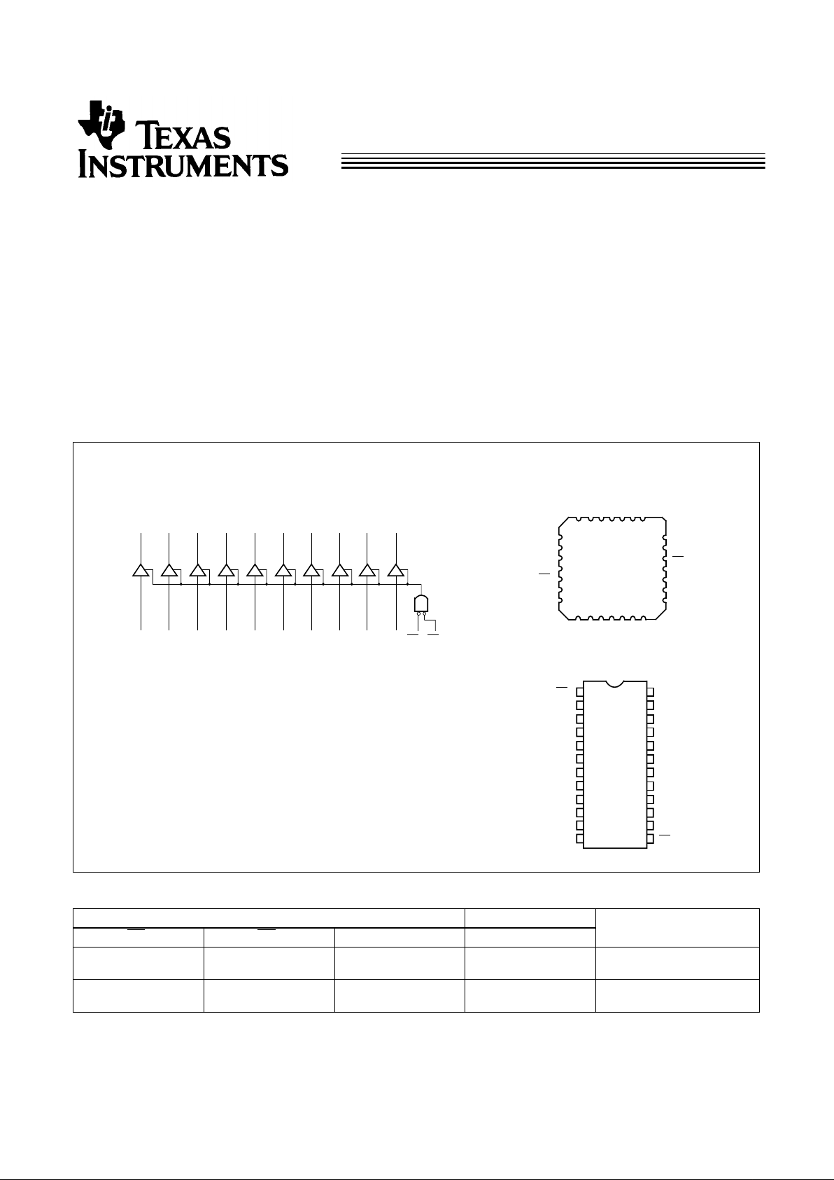
Logic Block Diagram Pin Configurations
Y
0
OE
1
Y1Y2Y3Y4Y
5
Y8Y
9
Y6Y
7
D0D1D2D3D4D
5
D8D
9
D6D
7
28
4
5678910
3
2
1
27
13
14
15
16
17
26
2524232221
20
11
12
19
D
4
D6D
5
Y
2
Y
5
18
NC
NC
Y
6
D
3
LCC/PLCC
Top View
NC
GND
Y
4
V
CC
D
8
D
9
Y
8
Y
9
OE
2
D
7
D
2
NC
OE
2
Y
3
Y
7
D
0
D
1
OE
1
Y
1
Y
0
1
2
3
4
5
6
7
8
9
10
11
12
16
17
18
19
20
24
23
22
21
13
14
V
CC
15
SOIC/QSOP
Top View
OE
1
D
1
D
2
D
3
D
4
D
5
D
6
D
7
D
8
Y
1
Y
2
Y
3
Y
4
Y
5
Y
6
Y
7
Y
8
GND
D
0
D
9
Y
0
Y
9
OE
2
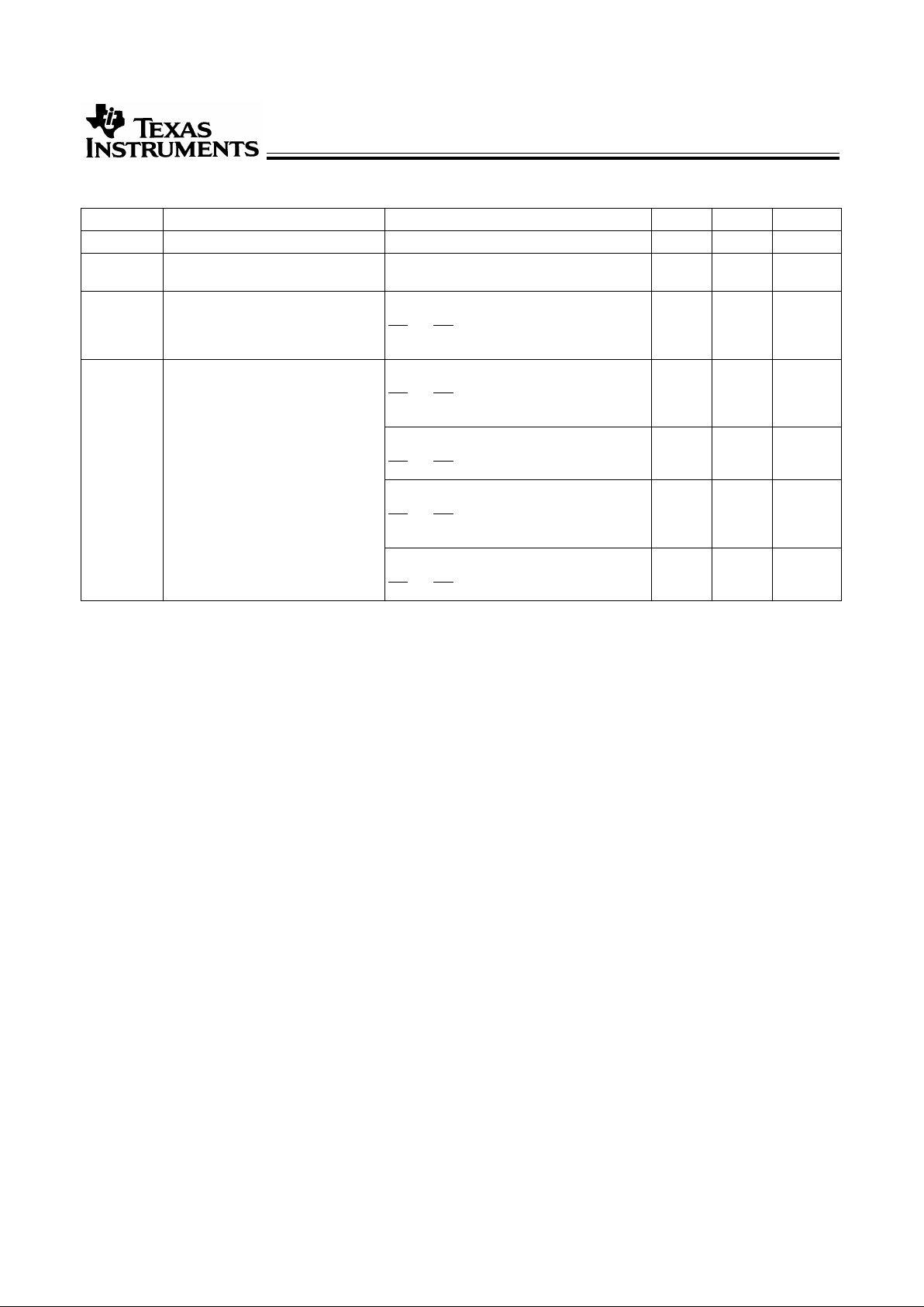
Function Table
[1]
Inputs Outputs
FunctionOE
1
OE
2
D Y
L
L
L
L
L
H
L
H
Transparent
H
X
X
H
X
X
Z
Z
Three-State
Note:
1. H = HIGH Voltage Level. L = LOW Voltage Level. X = Don’t Care

CY54/74FCT827T
2
Maximum Ratings
[2, 3]
(Above which the useful life may be impaired. For user guidelines, not tested.)
Storage Temperature .................................–65°C to +150°C
Ambient Temperature with
Power Applied.............................................–65°C to +135°C
Supply Voltage to Ground Potential...............–0.5V to +7.0V
DC Input Voltage............................................–0.5V to +7.0V
DC Output Voltage......................................... –0.5V to +7.0V
DC Output Current (Maximum Sink Current/Pin).......120 mA
Power Dissipation..........................................................0.5W
Static Discharge Voltage............................................>2001V
(per MIL-STD-883, Method 3015)
Operating Range
Range Range
Ambient
Temperature V
CC
Commercial All –40°C to + 85°C 5V ± 5%
Military
[4]
All –55°C to +125°C 5V ± 10%
Electrical Characteristics Over the Operating Range
Parameter Description Test Conditions Min. Typ.
[5]
Max. Unit
V
OH
Output HIGH Voltage VCC= Min., IOH= –32 mA Com’l 2.0 V
VCC= Min., IOH= –15 mA Com’l 2.4 3.3 V
VCC= Min., IOH= –12 mA Mil 2.4 3.3 V
V
OL
Output LOW Voltage VCC= Min., IOL= 64 mA Com’l 0.3 0.55 V
VCC= Min., IOL= 32 mA Mil 0.3 0.55 V
V
IH
Input HIGH Voltage 2.0 V
V
IL
Input LOW Voltage 0.8 V
V
H
Hysteresis
[6]
All inputs 0.2 V
V
IK
Input Clamp Diode Voltage VCC= Min., IIN= –18 mA –0.7 –1.2 V
I
I
Input HIGH Current VCC= Max., VIN= V
CC
5 µA
I
IH
Input HIGH Current VCC= Max., VIN= 2.7V ±1 µA
I
IL
Input LOW Current VCC= Max., VIN= 0.5V ±1 µA
I
OZH
Off State HIGH-Level Output
Current
VCC= Max., V
OUT
= 2.7V 10 µA
I
OZL
Off State LOW-Level
Output Current
VCC = Max., V
OUT
= 0.5V –10 µA
I
OS
Output Short Circuit Current
[7]
VCC= Max., V
OUT
= 0.0V –60 –120 –225 mA
I
OFF
Power-Off Disable VCC= 0V, V
OUT
= 4.5V ±1 µA
Capacitance
[6]
Parameter Description Typ.
[5]
Max. Unit
C
IN
Input Capacitance 5 10 pF
C
OUT
Output Capacitance 9 12 pF
Notes:
2. Unless otherwise noted, these limits are over the operating free-air temperature range.
3. Unused inputs must always be connected to an appropriate logic voltage level, preferably either V
CC
or ground.
4. T
A
is the “instant on” case temperature.
5. Typical values are at V
CC
=5.0V, TA=+25˚C ambient.
6. This parameter is specified but not tested.
7. Not more than one output should be shorted at a time. Durationof short should not exceedone second. The use of high-speed test apparatus and/or sample
and hold techniques are preferable in order to minimize internal chip heating and more accurately reflect operational values. Otherwise prolonged shorting of
a high output may raise the chip temperature well above normal and thereby cause invalid readings in other parametric tests. In any sequence of parameter
tests, I
OS
tests should be performed last.
CY54/74FCT827T
3
Power Supply Characteristics
Parameter Description Test Conditions Typ.
[5]
Max. Unit
I
CC
Quiescent Power Supply Current VCC=Max., VIN≤0.2V, VIN≥VCC–0.2V 0.1 0.2 mA
∆I
CC
Quiescent Power Supply Current
(TTL inputs HIGH)
VCC=Max., VIN=3.4V,
[8]
f1=0, Outputs Open
0.5 2.0 mA
I
CCD
Dynamic Power Supply
Current
[9]
VCC=Max., One Input Toggling,
50% Duty Cycle, Outputs Open,
OE1 or OE2=GND,
V
IN
≤0.2V or VIN≥VCC–0.2V
0.06 0.12 mA/MHz
I
C
Total Power Supply Current
[10]
VCC=Max., 50% Duty Cycle, OutputsOpen,
One Bit Toggling at f
1
=10 MHz,
OE1 or OE2=GND,
V
IN
≤0.2V or VIN≥VCC–0.2V
0.7 1.4 mA
VCC=Max.,50% Duty Cycle, Outputs Open,
One Bit Toggling at f
1
=10 MHz,
OE1 or OE2=GND, VIN=3.4V or VIN=GND
1.0 2.4 mA
VCC=Max., 50% Duty Cycle, OutputsOpen,
Ten Bits Toggling at f
1
=2.5 MHz,
OE1 or OE2=GND,
V
IN
≤0.2V or VIN≥VCC–0.2V
1.6 3.2
[11]
mA
VCC=Max., 50% Duty Cycle, OutputsOpen,
Ten Bits Toggling at f
1
=2.5 MHz,
OE1 or OE2=GND,VIN=3.4V or VIN=GND
4.1 13.2
[11]
mA
Notes:
8. Per TTL driven input (V
IN
=3.4V); all other inputs at VCC or GND.
9. This parameter is not directly testable, but is derived for use in Total Power Supply calculations.
10. I
C
=I
QUIESCENT
+ I
INPUTS
+ I
DYNAMIC
IC=ICC+∆ICCDHNT+I
CCD(f0
/2 + f1N1)
I
CC
= Quiescent Current with CMOS input levels
∆I
CC
= Power Supply Current for a TTL HIGH input VIN=3.4V)
D
H
= Duty Cycle for TTL inputs HIGH
N
T
= Number of TTL inputs at D
H
I
CCD
= Dynamic Current caused by an input transition pair HLH or LHL)
f
0
= Clock frequency for registered devices, otherwise zero
f
1
= Input signal frequency
N
1
= Number of inputs changing at f
1
All currents are in milliamps and all frequencies are in megahertz.
11. Values for these conditions are examples of the ICC formula. These limits are specified but not tested.
 Loading...