


 Loading...
DRV8312
DRV8332
www.ti.com |
SLES256 –MAY 2010 |
Three Phase PWM Motor Driver
Check for Samples: DRV8312, DRV8332
FEATURES
•High-Efficiency Power Stage (up to 97%) with Low RDS(on) MOSFETs (80 mΩ at TJ = 25°C)
•Operating Supply Voltage up to 50 V (70 V Absolute Maximum)
•DRV8312 (power pad down): up to 3.5 A Continuous Phase Current (6.5 A Peak)
•DRV8332 (power pad up): up to 8 A Continuous Phase Current ( 13 A Peak)
•Independent Control of Three Phases
•PWM Operating Frequency up to 500 kHz
•Integrated Self-Protection Circuits Including Undervoltage, Overtemperature, Overload, and Short Circuit
•Programmable Cycle-by-Cycle Current Limit Protection
•Independent Supply and Ground Pins for Each Half Bridge
•Intelligent Gate Drive and Cross Conduction Prevention
•No External Snubber or Schottky Diode is Required
APPLICATIONS
•BLDC Motors
•Three Phase Permanent Magnet Synchronous Motors
•Inverters
•Half Bridge Drivers
•Robotic Control Systems
DESCRIPTION
The DRV8312/32 are high performance, integrated three phase motor drivers with an advanced protection system.
Because of the low RDS(on) of the power MOSFETs and intelligent gate drive design, the efficiency of
these motor drivers can be up to 97%, which enables the use of smaller power supplies and heatsinks, and are good candidates for energy efficient applications.
The DRV8312/32 require two power supplies, one at 12 V for GVDD and VDD, and another up to 50 V for PVDD. The DRV8312/32 can operate at up to 500-kHz switching frequency while still maintain precise control and high efficiency. They also have an innovative protection system safeguarding the device against a wide range of fault conditions that could damage the system. These safeguards are short-circuit protection, overcurrent protection, undervoltage protection, and two-stage thermal protection. The DRV8312/32 have a current-limiting circuit that prevents device shutdown during load transients such as motor start-up. A programmable overcurrent detector allows adjustable current limit and protection level to meet different motor requirements.
The DRV8312/32 have unique independent supply and ground pins for each half bridge, which makes it possible to provide current measurement through external shunt resistor and support half bridge drivers with different power supply voltage requirements.
Simplified Application Diagram
PVDD
GVDD |
|
|
|
GVDD_B |
GVDD_A |
|
OTW |
BST_A |
|
FAULT |
PVDD_A |
|
PWM_A |
OUT_A |
|
RESET_A |
GND_A |
|
|
M |
|
PWM_B |
GND_B |
CONTROLLER |
OC_ADJ |
OUT_B |
|
GND |
PVDD_B |
|
AGND |
BST_B |
|
VREG |
NC |
|
M3 |
NC |
|
M2 |
GND |
|
M1 |
GND |
|
PWM_C |
GND_C |
|
RESET_C |
OUT_C |
|
RESET_B PVDD_C |
|
GVDD |
VDD |
BST_C |
|
GVDD_C |
GVDD_C |
Please be aware that an important notice concerning availability, standard warranty, and use in critical applications of Texas Instruments semiconductor products and disclaimers thereto appears at the end of this data sheet.
PRODUCTION DATA information is current as of publication date. |
Copyright © 2010, Texas Instruments Incorporated |
Products conform to specifications per the terms of the Texas |
|
Instruments standard warranty. Production processing does not |
|
necessarily include testing of all parameters. |
|

DRV8312
DRV8332
SLES256 –MAY 2010 |
www.ti.com |
This integrated circuit can be damaged by ESD. Texas Instruments recommends that all integrated circuits be handled with appropriate precautions. Failure to observe proper handling and installation procedures can cause damage.
ESD damage can range from subtle performance degradation to complete device failure. Precision integrated circuits may be more susceptible to damage because very small parametric changes could cause the device not to meet its published specifications.
ABSOLUTE MAXIMUM RATINGS
Over operating free-air temperature range unless otherwise noted (1)
|
|
|
|
|
|
|
|
|
|
|
VALUE |
|
|
|
|||||||||
|
VDD to GND |
–0.3 V to 13.2 V |
|||||||||
|
|
|
|||||||||
|
GVDD_X to GND |
–0.3 V to 13.2 V |
|||||||||
|
|
|
|||||||||
|
PVDD_X to GND_X (2) |
–0.3 V to 70 V |
|||||||||
|
OUT_X to GND_X (2) |
–0.3 V to 70 V |
|||||||||
|
BST_X to GND_X (2) |
–0.3 V to 80 V |
|||||||||
|
Transient peak output current (per pin), pulse width limited by internal over-current protection circuit. |
16 A |
|||||||||
|
|
|
|||||||||
|
Transient peak output current for latch shut down (per pin) |
20 A |
|||||||||
|
|
|
|||||||||
|
VREG to AGND |
–0.3 V to 4.2 V |
|||||||||
|
|
|
|||||||||
|
GND_X to GND |
–0.3 V to 0.3 V |
|||||||||
|
|
|
|||||||||
|
GND to AGND |
–0.3 V to 0.3 V |
|||||||||
|
|
|
|
|
|||||||
|
PWM_X, |
|
|
to GND |
–0.3 V to 4.2 V |
||||||
|
RESET_X |
||||||||||
|
OC_ADJ, M1, M2, M3 to AGND |
–0.3 V to 4.2 V |
|||||||||
|
|
|
|
|
|
|
|
||||
|
|
|
|
|
to GND |
–0.3 V to 7 V |
|||||
|
FAULT, |
OTW |
|||||||||
|
Maximum continuous sink current |
|
|
|
|
9 mA |
|||||
(FAULT, |
OTW) |
||||||||||
|
Maximum operating junction temperature range, TJ |
-40°C to 150°C |
|||||||||
|
Storage temperature, TSTG |
–55°C to 150°C |
|||||||||
(1)Stresses beyond those listed under Absolute Maximum Ratings may cause permanent damage to the device. These are stress ratings only, and functional operation of the device at these or any other conditions beyond those indicated under Recommended Operating Conditions is not implied. Exposure to absolute-maximum-rated conditions for extended periods may affect device reliability.
(2)These voltages represent the dc voltage + peak ac waveform measured at the terminal of the device in all conditions.
RECOMMENDED OPERATING CONDITIONS
|
|
MIN |
NOM |
MAX |
UNIT |
|
|
|
|
|
|
PVDD_X |
Half bridge X (A, B, or C) DC supply voltage |
0 |
50 |
52.5 |
V |
|
|
|
|
|
|
GVDD_X |
Supply for logic regulators and gate-drive circuitry |
10.8 |
12 |
13.2 |
V |
|
|
|
|
|
|
VDD |
Digital regulator supply voltage |
10.8 |
12 |
13.2 |
V |
|
|
|
|
|
|
IO_PULSE |
Pulsed peak current per output pin (could be limited by thermal) |
|
|
15 |
A |
IO |
Continuous current per output pin (DRV8332) |
|
|
8 |
A |
FSW |
PWM switching frequency |
|
|
500 |
kHz |
ROCP_CBC |
OC programming resistor range in cycle-by-cycle current limit modes |
22 |
|
200 |
kΩ |
ROCP_OCL |
OC programming resistor range in OC latching shutdown modes |
19 |
|
200 |
kΩ |
CBST |
Bootstrap capacitor range |
33 |
|
220 |
nF |
TON_MIN |
Minimum PWM pulse duration, low side |
|
50 |
|
nS |
T |
Operating ambient temperature |
-40 |
|
85(1) |
°C |
A |
|
|
|
|
|
(1)Depending on power dissipation and heat-sinking, the DRV8312/32 can support ambient temperature in excess of 85°C. Refer to the package heat dissipation ratings table and package power deratings table.
2 |
Submit Documentation Feedback |
Copyright © 2010, Texas Instruments Incorporated |
Product Folder Link(s): DRV8312 DRV8332

|
DRV8312 |
|
DRV8332 |
www.ti.com |
SLES256 –MAY 2010 |
PACKAGE HEAT DISSIPATION RATINGS
PARAMETER |
DRV8312 |
DRV8332 |
|
|
|
RqJC, junction-to-case (power pad / heat slug) |
1.1 °C/W |
0.9 °C/W |
thermal resistance |
|
|
|
|
This device is not intended to be used |
RqJA, junction-to-ambient thermal resistance |
25 °C/W |
without a heatsink. Therefore, RqJA is not |
specified. See the Thermal Information |
||
|
|
section. |
|
|
|
Exposed power pad / heat slug area |
34 mm2 |
80 mm2 |
PACKAGE POWER DERATINGS (DRV8312)(1)
|
TA = 25°C |
DERATING |
|
|
|
|
PACKAGE |
FACTOR |
TA = 70°C POWER |
TA = 85°C POWER |
TA = 125°C POWER |
||
POWER |
||||||
|
RATING |
ABOVE TA = |
RATING |
RATING |
RATING |
|
|
|
25°C |
|
|
|
|
44-PIN TSSOP (DDW) |
5.0 W |
40.0 mW/°C |
3.2 W |
2.6 W |
1.0 W |
|
|
|
|
|
|
|
(1)Based on EVM board layout
MODE SELECTION PINS
|
MODE PINS |
|
OUTPUT |
DESCRIPTION |
||
M3 |
|
M2 |
|
M1 |
CONFIGURATION |
|
|
|
|
||||
|
|
|
|
|
|
|
1 |
|
0 |
|
0 |
1 3PH or 3 HB |
Three-phase or three half bridges with cycle-by-cycle current limit |
|
|
|
|
|
|
|
1 |
|
0 |
|
1 |
1 3PH or 3 HB |
Three-phase or three half bridges with OC latching shutdown (no |
|
|
cycle-by-cycle current limit) |
||||
|
|
|
|
|
|
|
|
|
|
|
|
|
|
0 |
|
x |
|
x |
|
Reserved |
|
|
|
|
|
|
|
1 |
|
1 |
|
x |
|
Reserved |
|
|
|
|
|
|
|
Copyright © 2010, Texas Instruments Incorporated |
Submit Documentation Feedback |
3 |
Product Folder Link(s): DRV8312 DRV8332
DRV8312
DRV8332
SLES256 –MAY 2010 |
www.ti.com |
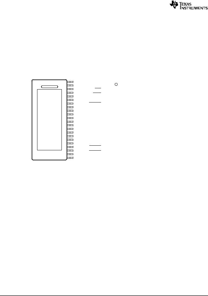
DEVICE INFORMATION
Pin Assignment
Here are the pinouts for the DRV8312/32:
•DRV8312: 44-pin TSSOP power pad down DDW package. This package contains a thermal pad that is located on the bottom side of the device for dissipating heat through PCB.
•DRV8332: 36-pin PSOP3 DKD package. This package contains a thick heat slug that is located on the top side of the device for dissipating heat through heatsink.
|
|
|
|
|
|
|
|
|
|
|
DRV8312 |
|
|
|
|
|
|
|
|
|
|
|
DDW Package |
|
|
|
|
|
|
|
|
|
|
|
(Top View) |
GVDD_C |
|
1 |
44 |
||||||||
|
|
VDD |
|
2 |
43 |
||||||
|
|
|
|
||||||||
|
|
NC |
|
3 |
42 |
||||||
|
|
NC |
|
4 |
41 |
||||||
PWM_C |
|
5 |
40 |
||||||||
|
|
|
|
||||||||
|
|
|
|
|
|
|
|
|
|||
RESET_C |
|
|
|
|
6 |
39 |
|||||
|
|
|
|
||||||||
|
|
|
|
|
|
|
|
||||
RESET_B |
|
|
|
|
7 |
38 |
|||||
|
|
M1 |
|
8 |
37 |
||||||
|
|
|
|
||||||||
|
|
M2 |
|
9 |
36 |
||||||
|
|
|
|
||||||||
|
|
M3 |
|
10 |
35 |
||||||
|
VREG |
|
|
|
|
11 |
34 |
||||
|
AGND |
|
12 |
33 |
|||||||
|
|
|
|
||||||||
|
|
GND |
|
13 |
32 |
||||||
OC_ADJ |
|
14 |
31 |
||||||||
PWM_B |
|
15 |
30 |
||||||||
|
|
|
|
||||||||
|
|
|
|
|
|
|
|||||
RESET_A |
|
|
|
|
16 |
29 |
|||||
PWM_A |
|
17 |
28 |
||||||||
|
|
|
|
|
18 |
27 |
|||||
FAULT |
|
|
|
|
|||||||
|
|
|
|
||||||||
|
|
NC |
|
19 |
26 |
||||||
|
|
|
|
||||||||
|
|
NC |
|
20 |
25 |
||||||
|
|
|
|
||||||||
|
|
|
|
|
21 |
24 |
|||||
|
OTW |
|
|
|
|
||||||
|
|
|
|
||||||||
GVDD_B |
|
22 |
23 |
||||||||
GVDD_C BST_C
NC PVDD_C PVDD_C OUT_C GND_C GND
GND
NC
NC BST_B PVDD_B OUT_B GND_B GND_A OUT_A PVDD_A PVDD_A NC BST_A GVDD_A
DRV8332
DKD Package
(Top View)
GVDD_B |
|
|
|
1 |
|
|
36 |
|
|
GVDD_A |
||
OTW |
|
|
|
2 |
|
|
35 |
|
|
BST_A |
||
|
|
|
|
|
|
|
||||||
FAULT |
|
|
|
3 |
|
|
|
34 |
|
|
PVDD_A |
|
|
|
|
|
|
|
|
|
|||||
PWM_A |
|
|
|
4 |
|
|
33 |
|
|
OUT_A |
||
RESET_A |
|
|
5 |
|
|
|
32 |
|
|
GND_A |
||
|
|
|
|
|
|
|
|
|
|
|||
PWM_B |
|
|
|
|
6 |
|
|
|
31 |
|
|
GND_B |
|
|
|
|
|
|
|
|
|
|
|
|
OUT_B |
OC_ADJ |
|
|
7 |
|
|
|
30 |
|
|
|||
GND |
|
|
|
|
8 |
|
|
|
29 |
|
|
PVDD_B |
AGND |
|
|
|
9 |
|
|
|
28 |
|
|
BST_B |
|
VREG |
|
|
|
10 |
|
|
|
27 |
|
|
NC |
|
|
|
|
|
|
|
|
||||||
|
|
|
|
|
|
|
|
|
|
|
|
|
M3 |
|
|
11 |
|
|
|
26 |
|
|
NC |
||
|
|
|
|
12 |
|
|
|
|
|
|
|
|
M2 |
|
|
|
|
|
25 |
|
|
GND |
|||
M1 |
|
|
13 |
|
|
|
24 |
|
|
GND |
||
RESET_B |
|
|
14 |
|
|
|
23 |
|
|
GND_C |
||
RESET_C |
|
|
15 |
|
|
|
22 |
|
|
OUT_C |
||
PWM_C |
|
|
16 |
|
|
|
21 |
|
|
PVDD_C |
||
|
|
|
|
|
|
|
||||||
VDD |
|
|
17 |
|
|
20 |
|
|
BST_C |
|||
|
|
|
|
|
|
|
||||||
GVDD_C |
|
|
18 |
|
|
19 |
|
|
GVDD_C |
|||
|
|
|
|
|
|
|
|
|
|
|
|
|
Pin Functions
|
PIN |
|
FUNCTION (1) |
DESCRIPTION |
|
|
|
|
|||
NAME |
DRV8312 |
DRV8332 |
|||
|
|
||||
|
|
|
|
|
|
AGND |
12 |
9 |
P |
Analog ground |
|
|
|
|
|
|
|
BST_A |
24 |
35 |
P |
High side bootstrap supply (BST), external capacitor to OUT_A required |
|
|
|
|
|
|
|
BST_B |
33 |
28 |
P |
High side bootstrap supply (BST), external capacitor to OUT_B required |
|
|
|
|
|
|
|
BST_C |
43 |
20 |
P |
High side bootstrap supply (BST), external capacitor to OUT_C required |
|
|
|
|
|
|
|
GND |
13, 36, 37 |
8 |
P |
Ground |
|
|
|
|
|
|
|
GND_A |
29 |
32 |
P |
Power ground for half-bridge A requires close decoupling capacitor to ground |
|
|
|
|
|
|
|
GND_B |
30 |
31 |
P |
Power ground for half-bridge B requires close decoupling capacitor to ground |
|
|
|
|
|
|
|
GND_C |
38 |
23 |
P |
Power ground for half-bridge C requires close decoupling capacitor to ground |
|
|
|
|
|
|
|
GVDD_A |
23 |
36 |
P |
Gate-drive voltage supply |
|
|
|
|
|
|
|
GVDD_B |
22 |
1 |
P |
Gate-drive voltage supply |
|
|
|
|
|
|
|
GVDD_C |
1, 44 |
18, 19 |
P |
Gate-drive voltage supply |
|
|
|
|
|
|
|
M1 |
8 |
13 |
I |
Mode selection pin |
|
|
|
|
|
|
|
M2 |
9 |
12 |
I |
Mode selection pin |
|
|
|
|
|
|
|
M3 |
10 |
11 |
I |
Reserved mode selection pin, AGND connection is recommended |
|
|
|
|
|
|
|
NC |
3,4,19,20,25,34,35 |
26,27 |
- |
No connection pin. Ground connection is recommended |
|
|
,42 |
|
|
|
|
|
|
|
|
|
|
OC_ADJ |
14 |
7 |
O |
Analog overcurrent programming pin, requires resistor to AGND |
|
|
|
|
|
|
(1)I = input, O = output, P = power, T = thermal
4 |
Submit Documentation Feedback |
Copyright © 2010, Texas Instruments Incorporated |
Product Folder Link(s): DRV8312 DRV8332

|
|
|
|
|
|
|
|
|
|
|
|
DRV8312 |
|
|
|
|
|
|
|
|
|
|
|
|
DRV8332 |
www.ti.com |
|
|
|
SLES256 –MAY 2010 |
||||||||
|
|
|
|
|
|
|
|
|
|
|
|
|
|
|
|
|
|
|
|
|
|
PIN |
|
FUNCTION (1) |
DESCRIPTION |
|
|
|
|
|
|
|
|
|
|
|
||
|
|
NAME |
DRV8312 |
DRV8332 |
||||||||
|
|
|
|
|||||||||
|
|
|
|
|
|
|
|
|
||||
|
|
|
|
|
21 |
2 |
O |
Overtemperature warning signal, open-drain, active-low. An internal pull-up resistor |
||||
|
|
|
OTW |
|||||||||
|
|
|
|
|
|
|
|
|
|
|
|
to VREG (3.3 V) is provided on output. Level compliance for 5-V logic can be |
|
|
|
|
|
|
|
|
|
|
|
|
obtained by adding external pull-up resistor to 5 V |
|
|
|
|
|
|
|
|
|||||
|
OUT_A |
28 |
33 |
O |
Output, half-bridge A |
|||||||
|
|
|
|
|
|
|
|
|||||
|
OUT_B |
31 |
30 |
O |
Output, half-bridge B |
|||||||
|
|
|
|
|
|
|
|
|||||
|
OUT_C |
39 |
22 |
O |
Output, half-bridge C |
|||||||
|
|
|
|
|
|
|
|
|||||
|
PVDD_A |
26,27 |
34 |
P |
Power supply input for half-bridge A requires close decoupling capacitor to ground. |
|||||||
|
|
|
|
|
|
|
|
|||||
|
PVDD_B |
32 |
29 |
P |
Power supply input for half-bridge B requires close decoupling capacitor to gound. |
|||||||
|
|
|
|
|
|
|
|
|||||
|
PVDD_C |
40,41 |
21 |
P |
Power supply input for half-bridge C requires close decoupling capacitor to ground. |
|||||||
|
|
|
|
|
|
|
|
|||||
|
PWM_A |
17 |
4 |
I |
Input signal for half-bridge A |
|||||||
|
|
|
|
|
|
|
|
|||||
|
PWM_B |
15 |
6 |
I |
Input signal for half-bridge B |
|||||||
|
|
|
|
|
|
|
|
|||||
|
PWM_C |
5 |
16 |
I |
Input signal for half-bridge C |
|||||||
|
|
|
|
|
|
|
|
|
||||
|
|
|
|
|
|
|
16 |
5 |
I |
Reset signal for half-bridge A, active-low |
||
|
RESET_A |
|||||||||||
|
|
|
|
|
|
|
|
|
|
|||
|
|
|
|
|
|
|
|
7 |
15 |
I |
Reset signal for half-bridge B, active-low |
|
|
RESET_B |
|||||||||||
|
|
|
|
|
|
|
|
|
6 |
15 |
I |
Reset signal for half-bridge C, active-low |
|
RESET_C |
|||||||||||
|
|
|
|
|
|
|
|
|
|
|
|
|
|
|
|
|
|
|
|
|
|
18 |
3 |
O |
Fault signal, open-drain, active-low. An internal pull-up resistor to VREG (3.3 V) is |
|
|
FAULT |
||||||||||
|
|
|
|
|
|
|
|
|
|
|
|
provided on output. Level compliance for 5-V logic can be obtained by adding |
|
|
|
|
|
|
|
|
|
|
|
|
external pull-up resistor to 5 V |
|
|
|
|
|
|
|
|
|
|
|
|
|
|
|
|
VDD |
2 |
17 |
P |
Power supply for digital voltage regulator requires capacitor to ground for |
|||||
|
|
|
|
|
|
|
|
|
|
|
|
decoupling. |
|
|
|
|
|
|
|
|
|
|
|
|
|
|
|
VREG |
11 |
10 |
P |
Digital regulator supply filter pin requires 0.1-mF capacitor to AGND. |
||||||
|
|
|
|
|
|
|
|
|
|
|
|
|
THERMAL PAD |
-- |
N/A |
T |
Solder the exposed thermal pad at the bottom of the DRV8312DDW package to the |
||||||||
|
|
|
|
|
|
|
|
|
|
|
|
landing pad on the PCB. Connect the landing pad through vias to large ground |
|
|
|
|
|
|
|
|
|
|
|
|
plate for better thermal dissipation. |
|
|
|
|
|
|
|
|
|
|
|
|
|
HEAT SLUG |
N/A |
-- |
T |
Mount heatsink with thermal interface to the heat slug on the top of the |
||||||||
|
|
|
|
|
|
|
|
|
|
|
|
DRV8332DKD package to improve thermal dissipation. |
|
|
|
|
|
|
|
|
|
|
|
|
|
Copyright © 2010, Texas Instruments Incorporated |
Submit Documentation Feedback |
5 |
Product Folder Link(s): DRV8312 DRV8332
DRV8312
DRV8332
SLES256 –MAY 2010 www.ti.com
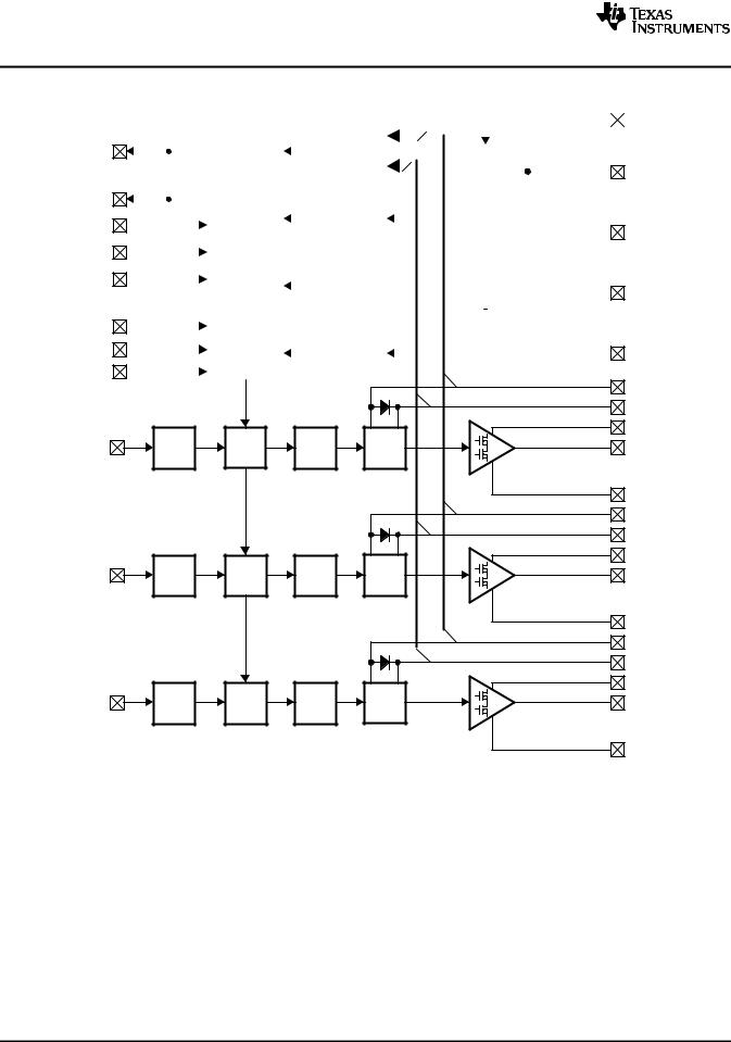
SYSTEM BLOCK DIAGRAM
|
|
|
|
|
|
|
|
|
|
|
|
4 |
|
|
|
|
|
|
|
|
|
|
|
|
VDD |
||
|
|
|
|
|
|
|
|
|
|
|
Under- |
|
|
|
|
|
|
|
|
|
|
|
|
|
|
|
|
|
|
|
|
|
|
|
|
|
|
|
|
|
|
|
|
|
|
|
|
|
|
|
|
|
|
|
|
|
|
OTW |
|
|
|
|
|
|
voltage |
4 |
|
|
|
|
|
|
|
|
|
|
|
|
|
|
|||
|
|
|
|
|
|
|
|
|
|
|
|
|
|
|
|
|
|||||||||||
|
|
|
|
|
|
|
|
|
|
|
Protection |
|
|
|
|
|
VREG |
|
|
|
|
VREG |
|||||
|
|
|
|
|
|
Internal Pullup |
|
|
|
|
|
|
|
|
|
|
|
|
|
||||||||
|
|
|
|
|
|
|
|
|
|
|
|
|
|
|
|
|
|||||||||||
|
|
|
|
|
|
Resistors to VREG |
|
|
|
|
|
|
|
|
|
|
|
|
|
|
|
|
|
|
|
|
|
|
|
|
|
|
|
|
|
|
|
|
|
|
|
|
|
|
|
|
|
|
|
|
|
|
|
|
|
FAULT |
|
|
|
|
|
Power |
|
|
|
|
|
|
|
|
|
|
|
|
|
|
|
|
|||||
|
|
|
|
|
|
|
|
|
|
|
|
|
|
|
|
|
|
|
|
|
|
|
|
|
|
|
|
|
|
M1 |
|
|
|
|
|
|
On |
|
|
|
|
|
|
|
|
|
|
|
|
|
|
|
|
||
|
|
|
|
|
|
|
|
|
|
|
|
|
|
|
|
|
|
|
|
|
|
|
|
||||
|
|
|
|
|
Protection |
|
Reset |
|
|
|
|
|
|
|
|
|
|
|
|
|
|
|
AGND |
||||
|
|
|
|
|
|
|
|
|
|
|
|
|
|
|
|
|
|
|
|||||||||
|
|
|
|
|
|
|
|
|
|
|
|
|
|
|
|
|
|
|
|
|
|
|
|
|
|||
|
|
|
|
|
|
|
|
|
|
|
|
|
|
|
|
|
|
|
|
|
|
|
|
|
|||
|
|
|
|
|
|
|
|
|
|
|
|
|
|
|
|
|
|
|
|
|
|
|
|
|
|
|
|
|
|
M2 |
|
|
|
|
and |
|
|
|
|
|
|
|
|
|
|
|
|
|
|
|
|
|
|
||
|
|
|
|
|
|
|
|
|
|
|
|
|
|
|
|
|
|
|
|
|
|||||||
|
|
|
|
|
|
|
|
|
I/O Logic |
|
|
|
|
|
|
|
|
|
|
|
|
|
|
|
|
|
|
|
|
M3 |
|
|
|
|
Temp. |
|
|
|
|
|
|
|
|
|
|
|
|
|
|
|
|
||||
|
|
|
|
|
|
|
|
|
|
|
|
|
|
|
|
|
|
|
|
|
|
||||||
|
|
|
|
|
|
|
|
|
|
|
Sense |
|
|
|
|
|
|
|
|
|
|
|
|
|
|
|
GND |
|
|
|
|
|
|
|
|
|
|
|
|
|
|
|
|
|
|
|
|
|
|
|
|
|
|
|
|
|
|
|
|
|
|
|
|
|
|
|
|
|
|
|
|
|
|
|
|
|
|
|
|
|
|
|
|
|
|
|
|
|
|
|
|
|
|
|
|
|
|
|
|
|
|
|
|
|
|
|
|
|
|
|
|
|
|
|
|
|
|
|
|
|
|
|
|
|
|
|
|
|
|
|
|
|
|
|
|
|
|
|
|
RESET_A |
|
|
|
|
|
|
|
|
|
|
|
|
|
|
|
|
|
|
|
|
|
|
|
||||
|
|
|
|
|
|
Overload |
|
|
|
|
|
|
|
|
|
|
|
|
|
|
|
|
|||||
|
|
|
|
|
|
|
|
|
|
|
|
|
|
|
|
|
|
|
|
|
|
|
|
|
|
|
|
RESET_B |
|
|
|
|
|
|
|
|
|
|
|
|
|
Isense |
|
|
|
OC_ADJ |
|||||||||
|
|
|
|
Protection |
|
|
|
|
|
|
|
|
|
|
|||||||||||||
|
|
|
|
|
|
|
|
|
|
|
|
|
|
|
|
|
|
|
|
|
|||||||
|
|
|
|
|
|
|
|
|
|
|
|
|
|
|
|
|
|
|
|
|
|
|
|
|
|
|
|
RESET_C |
|
|
|
|
|
|
|
|
|
|
|
|
|
|
|
|
|
|
|
|
|
|
|
||||
|
|
|
|
|
|
|
|
|
|
|
|
|
|
|
|
|
|
|
|
||||||||
|
|
|
|
|
|
|
|
|
|
|
|
|
|
|
|
|
|
|
|
|
|
|
|
|
|
|
|
|
|
|
|
|
GVDD_C |
|
|
|
|
|
|
BST_C |
|
|
|
|
|
|
PVDD_C |
|
PWM_C |
PWM |
Ctrl. |
Timing |
Gate |
OUT_C |
|
Rcv. |
Drive |
|||||
|
|
|
|
|||
|
|
|
|
|
GND_C |
|
|
|
|
|
|
GVDD_B |
|
|
|
|
|
|
BST_B |
|
|
|
|
|
|
PVDD_B |
|
PWM_B |
PWM |
Ctrl. |
Timing |
Gate |
OUT_B |
|
Rcv. |
Drive |
|||||
|
|
|
|
|||
|
|
|
|
|
GND_B |
|
|
|
|
|
|
GVDD_A |
|
|
|
|
|
|
BST_A |
|
|
|
|
|
|
PVDD_A |
|
PWM_A |
PWM |
Ctrl. |
Timing |
Gate |
OUT_A |
|
Rcv. |
Drive |
|||||
|
|
|
|
|||
|
|
|
|
|
GND_A |
6 |
Submit Documentation Feedback |
Copyright © 2010, Texas Instruments Incorporated |
Product Folder Link(s): DRV8312 DRV8332

DRV8312
DRV8332
www.ti.com |
SLES256 –MAY 2010 |
ELECTRICAL CHARACTERISTICS
TA = 25 °C, PVDD = 50 V, GVDD = VDD = 12 V, fSw = 400 kHz, unless otherwise noted. All performance is in accordance with recommended operating conditions unless otherwise specified.
|
PARAMETER |
|
|
|
TEST CONDITIONS |
MIN |
TYP |
MAX |
UNIT |
|||||||||||
|
|
|
|
|
|
|
|
|
|
|
|
|||||||||
Internal Voltage Regulator and Current Consumption |
|
|
|
|
|
|
|
|
|
|
|
|||||||||
|
|
|
|
|
|
|
|
|||||||||||||
VREG |
Voltage regulator, only used as a reference node |
|
VDD = 12 V |
2.95 |
3.3 |
3.65 |
V |
|||||||||||||
IVDD |
VDD supply current |
|
Idle, reset mode |
|
9 |
12 |
mA |
|||||||||||||
|
|
|
|
|
|
|
|
|
|
|
||||||||||
|
Operating, 50% duty cycle |
|
10.5 |
|
|
|||||||||||||||
|
|
|
|
|
|
|
|
|
|
|
|
|
|
|||||||
|
|
|
|
|
|
|
|
|
|
|
|
|
|
|
|
|||||
IGVDD_X |
Gate supply current per half-bridge |
|
Reset mode |
|
1.7 |
2.5 |
mA |
|||||||||||||
|
|
|
|
|
|
|
|
|
|
|
||||||||||
|
Operating, 50% duty cycle |
|
8 |
|
|
|||||||||||||||
|
|
|
|
|
|
|
|
|
|
|
|
|
|
|||||||
|
|
|
|
|
|
|
|
|||||||||||||
IPVDD_X |
Half-bridge X (A, B, or C) idle current |
|
Reset mode |
|
0.7 |
1 |
mA |
|||||||||||||
Output Stage |
|
|
|
|
|
|
|
|
|
|
|
|
|
|
|
|
|
|
|
|
|
|
|
|
|
|
|
|
|||||||||||||
RDS(on) |
MOSFET drain-to-source resistance, low side (LS) |
|
TJ = 25°C, GVDD = 12 V |
|
80 |
|
mΩ |
|||||||||||||
MOSFET drain-to-source resistance, high side (HS) |
|
TJ = 25°C, GVDD = 12 V |
|
80 |
|
mΩ |
||||||||||||||
|
|
|
|
|||||||||||||||||
VF |
Diode forward voltage drop |
|
TJ = 25°C - 125°C, IO = 5 A |
|
1 |
|
V |
|||||||||||||
tR |
Output rise time |
|
Resistive load, IO = 5 A |
|
14 |
|
nS |
|||||||||||||
tF |
Output fall time |
|
Resistive load, IO = 5 A |
|
14 |
|
nS |
|||||||||||||
tPD_ON |
Propagation delay when FET is on |
|
Resistive load, IO = 5 A |
|
38 |
|
nS |
|||||||||||||
tPD_OFF |
Propagation delay when FET is off |
|
Resistive load, IO = 5 A |
|
38 |
|
nS |
|||||||||||||
tDT |
Dead time between HS and LS FETs |
|
Resistive load, IO = 5 A |
|
5.5 |
|
nS |
|||||||||||||
I/O Protection |
|
|
|
|
|
|
|
|
|
|
|
|
|
|
|
|
|
|
|
|
|
|
|
|
|
|
|
|
|
|
|
|
|
|
|
|
|
||||
Vuvp,G |
Gate supply voltage GVDD_X undervoltage |
|
|
|
|
|
|
|
|
8.5 |
|
V |
||||||||
protection threshold |
|
|
|
|
|
|
|
|
|
|||||||||||
|
|
|
|
|
|
|
|
|
|
|
|
|||||||||
|
|
|
|
|
|
|
|
|
|
|
|
|
|
|
|
|
|
|
|
|
(1) |
Hysteresis for gate supply undervoltage event |
|
|
|
|
|
|
|
|
0.8 |
|
V |
||||||||
Vuvp,hyst |
|
|
|
|
|
|
|
|
|
|||||||||||
OTW(1) |
Overtemperature warning |
|
|
|
|
|
|
|
115 |
125 |
135 |
°C |
||||||||
(1) |
|
|
|
|
|
|
|
|
|
|
|
|
|
|
|
|
|
|
|
|
Hysteresis temperature to reset OTW event |
|
|
|
|
|
|
|
|
25 |
|
°C |
|||||||||
OTWhyst |
|
|
|
|
|
|
|
|
|
|||||||||||
OTSD(1) |
Overtemperature shut down |
|
|
|
|
|
|
|
|
150 |
|
°C |
||||||||
OTE- |
OTE-OTW overtemperature detect temperature |
|
|
|
|
|
|
|
|
25 |
|
°C |
||||||||
(1) |
difference |
|
|
|
|
|
|
|
|
|
||||||||||
OTWdifferential |
|
|
|
|
|
|
|
|
|
|
|
|||||||||
|
Hysteresis temperature for |
|
|
|
to be released |
|
|
|
|
|
|
|
|
|
|
|
||||
(1) |
FAULT |
|
|
|
|
|
|
|
|
25 |
|
°C |
||||||||
OTSDHYST |
following an OTSD event |
|
|
|
|
|
|
|
|
|
||||||||||
|
|
|
|
|
|
|
|
|
|
|
|
|||||||||
|
|
|
|
|
|
|
|
|
|
|
|
|||||||||
IOC |
Overcurrent limit protection |
|
Resistor— programmable, nominal, ROCP = 27 kΩ |
|
9.7 |
|
A |
|||||||||||||
IOCT |
Overcurrent response time |
|
Time from application of short condition to Hi-Z of |
|
250 |
|
ns |
|||||||||||||
|
affected FET(s) |
|
|
|||||||||||||||||
|
|
|
|
|
|
|
|
|
|
|
|
|
|
|
||||||
|
|
|
|
|
|
|
|
|
|
|
|
|
|
|
|
|
||||
Static Digital Specifications |
|
|
|
|
|
|
|
|
|
|
|
|||||||||
|
|
|
|
|
|
|
|
|
|
|
|
|
|
|
|
|
||||
VIH |
High-level input voltage |
|
PWM_A, PWM_B, PWM_C, M1, M2, M3 |
2 |
|
3.6 |
V |
|||||||||||||
VIH |
High-level input voltage |
|
|
|
|
|
|
|
2 |
|
3.6 |
V |
||||||||
|
RESET_A, RESET_B, RESET_C |
|
||||||||||||||||||
VIL |
Low-level input voltage |
|
PWM_A, PWM_B, PWM_C, M1, M2, M3, |
|
|
0.8 |
V |
|||||||||||||
|
|
|
|
|
|
|
|
|
||||||||||||
|
RESET_A, RESET_B, RESET_C |
|
|
|||||||||||||||||
|
|
|
|
|
|
|
|
|
|
|
|
|
|
|
||||||
llkg |
Input leakage current |
|
|
|
|
|
|
|
-100 |
|
100 |
mA |
||||||||
OTW / FAULT |
|
|
|
|
|
|
|
|
|
|
|
|
|
|
|
|
|
|
|
|
|
|
|
|
|
|
|
|
|
|
|
|
|
|
|
|
|
|
|
|
|
RINT_PU |
Internal pullup resistance, |
OTW |
|
to VREG, |
FAULT |
to |
|
|
|
|
|
|
|
20 |
26 |
35 |
kΩ |
|||
VREG |
|
|
|
|
|
|
|
|||||||||||||
|
|
|
|
|
|
|
|
|
|
|
|
|||||||||
|
|
|
|
|
|
|
|
|
|
|
|
|
|
|
|
|
|
|
|
|
VOH |
High-level output voltage |
|
Internal pullup resistor only |
2.95 |
3.3 |
3.65 |
V |
|||||||||||||
|
|
|
|
|
|
|
|
|
|
|||||||||||
|
External pullup of 4.7 kΩ to 5 V |
4.5 |
|
5 |
||||||||||||||||
|
|
|
|
|
|
|
|
|
|
|
|
|
||||||||
VOL |
Low-level output voltage |
|
IO = 4 mA |
|
0.2 |
0.4 |
V |
|||||||||||||
(1)Specified by design
Copyright © 2010, Texas Instruments Incorporated |
Submit Documentation Feedback |
7 |
Product Folder Link(s): DRV8312 DRV8332

DRV8312
DRV8332
SLES256 –MAY 2010 |
www.ti.com |
TYPICAL CHARACTERISTICS
EFFICIENCY vs
SWITCHING FREQUENCY (DRV8332)
|
100 |
|
|
|
|
|
|
|
|
|
|
|
90 |
|
|
|
|
|
|
|
|
|
|
|
80 |
|
|
|
|
|
|
|
|
|
|
|
70 |
|
|
|
|
|
|
|
|
|
|
% |
60 |
|
|
|
|
|
|
|
|
|
|
– |
|
|
|
|
|
|
|
|
|
|
|
|
|
|
|
|
|
|
|
|
|
|
|
Efficiency |
50 |
|
|
|
|
|
|
|
|
|
|
40 |
|
|
|
|
|
|
|
|
|
|
|
|
|
|
|
|
|
|
|
|
|
|
|
|
30 |
|
|
|
|
|
|
|
|
|
|
|
20 |
Full Bridge |
|
|
|
|
|
|
|
|
|
|
Load = 5 A |
|
|
|
|
|
|
|
|||
|
|
|
|
|
|
|
|
|
|||
|
10 |
PVDD = 50 V |
|
|
|
|
|
|
|
||
|
TC = 75°C |
|
|
|
|
|
|
|
|
||
|
0 |
|
|
|
|
|
|
|
|
|
|
|
0 |
50 |
100 |
150 |
200 |
250 |
300 |
350 |
400 |
450 |
500 |
f – Switching Frequency – kHz
Figure 1.
NORMALIZED RDS(on) vs
GATE DRIVE
|
1.10 |
|
|
|
|
|
|
|
|
|
|
|
|
|
|
|
TJ = 25°C |
|
|
AT 12 V) |
1.08 |
|
|
|
|
|
|
|
|
1.06 |
|
|
|
|
|
|
|
|
|
) |
|
|
|
|
|
|
|
|
|
DS(ON |
|
|
|
|
|
|
|
|
|
(R |
1.04 |
|
|
|
|
|
|
|
|
/ |
|
|
|
|
|
|
|
|
|
DS(ON) |
1.02 |
|
|
|
|
|
|
|
|
R |
|
|
|
|
|
|
|
|
|
NORMALIZED |
1.00 |
|
|
|
|
|
|
|
|
0.98 |
|
|
|
|
|
|
|
|
|
|
|
|
|
|
|
|
|
|
|
|
0.96 |
|
|
|
|
|
|
|
|
|
8.0 |
8.5 |
9.0 |
9.5 |
10.0 |
10.5 |
11.0 |
11.5 |
12 |
|
|
|
GVDD – GATE DRIVE – V |
|
|
||||
Figure 2.
NORMALIZED RDS(on) vs
JUNCTION TEMPERATURE
|
1.6 |
|
|
|
|
|
|
|
|
|
|
|
GVDD = 12 V |
|
|
|
|
|
|
||
C) |
1.4 |
|
|
|
|
|
|
|
|
|
o |
|
|
|
|
|
|
|
|
|
|
at25 |
|
|
|
|
|
|
|
|
|
|
DS(on) |
1.2 |
|
|
|
|
|
|
|
|
|
|
|
|
|
|
|
|
|
|
|
|
/(R |
|
|
|
|
|
|
|
|
|
|
DS(on) |
1.0 |
|
|
|
|
|
|
|
|
|
|
|
|
|
|
|
|
|
|
|
|
R |
|
|
|
|
|
|
|
|
|
|
Normalized |
0.8 |
|
|
|
|
|
|
|
|
|
0.6 |
|
|
|
|
|
|
|
|
|
|
|
0.4 |
|
|
|
|
|
|
|
|
|
|
–40 |
–20 |
0 |
20 |
40 |
60 |
80 |
100 |
120 |
140 |
|
|
|
T – Junction Temperature – oC |
|
|
|||||
|
|
|
J |
|
|
|
|
|
|
|
Figure 3.
DRAIN TO SOURCE DIODE FORWARD
ON CHARACTERISTICS
|
6 |
|
|
|
|
|
|
|
|
TJ = 25°C |
|
|
|
|
|
|
5 |
|
|
|
|
|
|
|
4 |
|
|
|
|
|
|
–A |
3 |
|
|
|
|
|
|
Current |
|
|
|
|
|
|
|
2 |
|
|
|
|
|
|
|
I– |
|
|
|
|
|
|
|
|
1 |
|
|
|
|
|
|
|
0 |
|
|
|
|
|
|
|
–1 |
|
|
|
|
|
|
|
0 |
0.2 |
0.4 |
0.6 |
0.8 |
1 |
1.2 |
|
|
|
V – Voltage – V |
|
|
||
Figure 4.
8 |
Submit Documentation Feedback |
Copyright © 2010, Texas Instruments Incorporated |
Product Folder Link(s): DRV8312 DRV8332
DRV8312
DRV8332
www.ti.com |
SLES256 –MAY 2010 |
TYPICAL CHARACTERISTICS (continued)
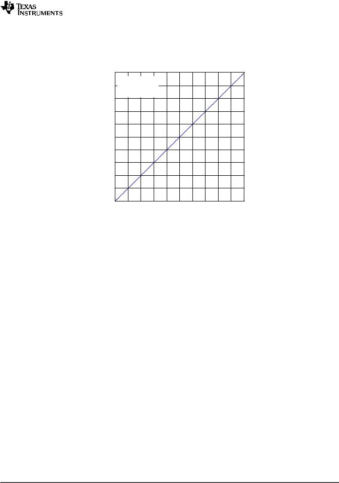
OUTPUT DUTY CYCLE vs
INPUT DUTY CYCLE
|
100 |
|
|
|
|
|
|
|
|
|
|
|
90 |
fS = 500 kHz |
|
|
|
|
|
|
|
||
|
TC = 25°C |
|
|
|
|
|
|
|
|
||
|
|
|
|
|
|
|
|
|
|
||
|
80 |
|
|
|
|
|
|
|
|
|
|
% |
70 |
|
|
|
|
|
|
|
|
|
|
– |
|
|
|
|
|
|
|
|
|
|
|
|
|
|
|
|
|
|
|
|
|
|
|
Cycle |
60 |
|
|
|
|
|
|
|
|
|
|
|
|
|
|
|
|
|
|
|
|
|
|
Duty |
50 |
|
|
|
|
|
|
|
|
|
|
|
|
|
|
|
|
|
|
|
|
|
|
Output |
40 |
|
|
|
|
|
|
|
|
|
|
30 |
|
|
|
|
|
|
|
|
|
|
|
|
20 |
|
|
|
|
|
|
|
|
|
|
|
10 |
|
|
|
|
|
|
|
|
|
|
|
0 |
|
|
|
|
|
|
|
|
|
|
|
0 |
10 |
20 |
30 |
40 |
50 |
60 |
70 |
80 |
90 |
100 |
Input Duty Cycle – %
Figure 5.
Copyright © 2010, Texas Instruments Incorporated |
Submit Documentation Feedback |
9 |
Product Folder Link(s): DRV8312 DRV8332

DRV8312
DRV8332
SLES256 –MAY 2010 |
www.ti.com |
THEORY OF OPERATION
POWER SUPPLIES
To facilitate system design, the DRV8312/32 need only a 12-V supply in addition to H-Bridge power supply (PVDD). An internal voltage regulator provides suitable voltage levels for the digital and low-voltage analog circuitry. Additionally, the high-side gate drive requiring a floating voltage supply, which is accommodated by built-in bootstrap circuitry requiring external bootstrap capacitor.
To provide symmetrical electrical characteristics, the PWM signal path, including gate drive and output stage, is designed as identical, independent half-bridges. For this reason, each half-bridge has a separate gate drive supply (GVDD_X), a bootstrap pin (BST_X), and a power-stage supply pin (PVDD_X). Furthermore, an additional pin (VDD) is provided as supply for all common circuits. Special attention should be paid to place all decoupling capacitors as close to their associated pins as possible. In general, inductance between the power supply pins and decoupling capacitors must be avoided. Furthermore, decoupling capacitors need a short ground path back to the device.
For a properly functioning bootstrap circuit, a small ceramic capacitor (an X5R or better) must be connected from each bootstrap pin (BST_X) to the power-stage output pin (OUT_X). When the power-stage output is low, the bootstrap capacitor is charged through an internal diode connected between the gate-drive power-supply pin (GVDD_X) and the bootstrap pin. When the power-stage output is high, the bootstrap capacitor potential is shifted above the output potential and thus provides a suitable voltage supply for the high-side gate driver. In an application with PWM switching frequencies in the range from 10 kHz to 500 kHz, the use of 100-nF ceramic capacitors (X5R or better), size 0603 or 0805, is recommended for the bootstrap supply. These 100-nF capacitors ensure sufficient energy storage, even during minimal PWM duty cycles, to keep the high-side power stage FET fully turned on during the remaining part of the PWM cycle. In an application running at a switching frequency lower than 10 kHz, the bootstrap capacitor might need to be increased in value.
Special attention should be paid to the power-stage power supply; this includes component selection, PCB placement, and routing. As indicated, each half-bridge has independent power-stage supply pin (PVDD_X). For optimal electrical performance, EMI compliance, and system reliability, it is important that each PVDD_X pin is decoupled with a ceramic capacitor (X5R or better) placed as close as possible to each supply pin. It is recommended to follow the PCB layout of the DRV8312/32 EVM board.
The 12-V supply should be from a low-noise, low-output-impedance voltage regulator. Likewise, the 50-V power-stage supply is assumed to have low output impedance and low noise. The power-supply sequence is not critical as facilitated by the internal power-on-reset circuit. Moreover, the DRV8312/32 are fully protected against erroneous power-stage turn-on due to parasitic gate charging. Thus, voltage-supply ramp rates (dv/dt) are non-critical within the specified voltage range (see the
Recommended Operating Conditions section of this data sheet).
SYSTEM POWER-UP/POWER-DOWN SEQUENCE
Powering Up
The DRV8312/32 do not require a power-up sequence. The outputs of the H-bridges remain in a high impedance state until the gate-drive supply voltage GVDD_X and VDD voltage are above the undervoltage protection (UVP) voltage threshold (see the Electrical Characteristics section of this data sheet). Although not specifically required, holding RESET_A, RESET_B, and RESET_C in a low state while powering up the device is recommended. This allows an internal circuit to charge the external bootstrap capacitors by enabling a weak pulldown of the half-bridge output.
Powering Down
The DRV8312/32 do not require a power-down sequence. The device remains fully operational as long as the gate-drive supply (GVDD_X) voltage and VDD voltage are above the UVP voltage threshold (see the Electrical Characteristics section of this data sheet). Although not specifically required, it is a good practice to hold RESET_A, RESET_B and RESET_C low during power down to prevent any unknown state during this transition.
10 |
Submit Documentation Feedback |
Copyright © 2010, Texas Instruments Incorporated |
Product Folder Link(s): DRV8312 DRV8332
Loading...