


 Loading...
Texas Instruments DRA756, DRA755, DRA754, DRA752, DRA751 Datasheet
...PRODUCT |
ORDER |
TECHNICAL |
TOOLS & |
Support & |
FOLDER |
NOW |
DOCUMENTS |
SOFTWARE |
Community |
DRA756, DRA755, DRA754, DRA752
DRA751, DRA750, DRA746, DRA745, DRA744
SPRS950F –DECEMBER 2015 –REVISED MAY 2019
DRA75x, DRA74x Infotainment Applications Processor
Silicon Revision 2.0
1 Device Overview
1.1Features
•Architecture designed for infotainment applications
•Video, image, and graphics processing support
–Full-HD video (1920 × 1080p, 60 fps)
–Multiple video input and video output
–2D and 3D graphics
•Dual Arm® Cortex®-A15 microprocessor subsystem
•Up to two C66x floating-point VLIW DSP
–Fully object-code compatible with C67x and C64x+
–Up to thirty-two 16 x 16-Bit fixed-point multiplies per cycle
•Up to 2.5MB of on-chip L3 RAM
•Level 3 (L3) and level 4 (L4) interconnects
•Two DDR2/DDR3/DDR3L memory interface (EMIF) modules
–Supports up to DDR2-800 and DDR3-1066
–Up to 2GB supported per EMIF
•Dual Arm® Cortex®-M4 Image Processing Units (IPU)
•Up to two Embedded Vision Engines (EVEs)
•IVA subsystem
•Display subsystem
–Display controller with DMA engine and up to three pipelines
–HDMI™ encoder: HDMI 1.4a and DVI 1.0 compliant
•Video Processing Engine (VPE)
•2D-graphics accelerator (BB2D) subsystem
–Vivante® GC320 core
•Dual-core PowerVR® SGX544 3D GPU
•Three Video Input Port (VIP) modules
–Support for up to 10 multiplexed input ports
•General-Purpose Memory Controller (GPMC)
•Enhanced Direct Memory Access (EDMA) controller
•2-port gigabit ethernet (GMAC)
•Sixteen 32-Bit general-purpose timers
•32-Bit MPU watchdog timer
•Five Inter-Integrated Circuit ( I2C™) ports
•HDQ™/ 1-Wire® interface
•SATA interface
•MediaLB® (MLB) subsystem
•Ten configurable UART/IrDA/CIR modules
•Four Multichannel Serial Peripheral Interfaces (McSPI)
•Quad SPI (QSPI)
•Eight Multichannel Audio Serial Port (McASP) modules
•SuperSpeed USB 3.0 dual-role device
•Three high-speed USB 2.0 dual-role devices
•Four Multimedia Card/Secure Digital/Secure Digital Input Output interfaces ( MMC™/ SD®/SDIO)
•PCI-Express® 3.0 subsystems with two 5-Gbps lanes
–One 2-lane gen2-compliant port
–or Two 1-lane gen2-compliant ports
•Dual Controller Area Network (DCAN) modules
–CAN 2.0B protocol
•Up to 247 General-Purpose I/O (GPIO) pins
•Real-Time Clock SubSystem (RTCSS)
•Device security features
–Hardware crypto accelerators and DMA
–Firewalls
–JTAG® lock
–Secure keys
–Secure ROM and boot
•Power, Reset, and Clock Management (PRCM)
•On-chip debug with CTools technology
•28-nm CMOS technology
•23 mm × 23 mm, 0.8-mm pitch, 760-pin BGA (ABC)
An IMPORTANT NOTICE at the end of this data sheet addresses availability, warranty, changes, use in safety-critical applications, intellectual property matters and other important disclaimers. PRODUCTION DATA.

DRA756, DRA755, DRA754, DRA752
DRA751, DRA750, DRA746, DRA745, DRA744
SPRS950F –DECEMBER 2015–REVISED MAY 2019 |
www.ti.com |
1.2Applications
• |
Human-machine interface (HMI) |
• |
Multimedia playback |
• |
Navigation |
• |
Web browsing |
• Digital and analog radio |
• |
ADAS integration |
|
•Rear seat entertainment
1.3Description
DRA75x and DRA74x (Jacinto 6) infotainment applications processors are built to meet the intense processing needs of the modern infotainment-enabled automobile experiences.
The device enables Original-Equipment Manufacturers (OEMs) and Original-Design Manufacturers (ODMs) to quickly implement innovative connectivity technologies, speech recognition, audio streaming, and more. Jacinto 6 devices bring high processing performance through the maximum flexibility of a fully integrated mixed processor solution. The devices also combine programmable video processing with a highly integrated peripheral set.
Programmability is provided by dual-core Arm® Cortex®-A15 RISC CPUs with Arm® Neon™ extension, TI C66x VLIW floating-point DSP core, and Vision AccelerationPac (with one or more EVEs). The Arm allows developers to keep control functions separate from other algorithms programmed on the DSP and coprocessors, thus reducing the complexity of the system software.
Additionally, TI provides a complete set of development tools for the Arm, DSP, and EVE coprocessor, including C compilers and a debugging interface for visibility into source code.
The DRA75x and DRA74x Jacinto 6 processor family is qualified according to the AEC-Q100 standard.
Device Information(1)
PART NUMBER |
PACKAGE |
BODY SIZE |
DRA756ABC |
FCBGA (760) |
23.0 mm × 23.0 mm |
DRA755ABC |
FCBGA (760) |
23.0 mm × 23.0 mm |
DRA754ABC |
FCBGA (760) |
23.0 mm × 23.0 mm |
DRA756ABC |
FCBGA (760) |
23.0 mm × 23.0 mm |
DRA755ABC |
FCBGA (760) |
23.0 mm × 23.0 mm |
DRA754ABC |
FCBGA (760) |
23.0 mm × 23.0 mm |
DRA752ABC |
FCBGA (760) |
23.0 mm × 23.0 mm |
DRA751ABC |
FCBGA (760) |
23.0 mm × 23.0 mm |
DRA750ABC |
FCBGA (760) |
23.0 mm × 23.0 mm |
(1)For more information, see Section 10, Mechanical, Packaging, and Orderable Information.
2 |
Device Overview |
Copyright © 2015–2019, Texas Instruments Incorporated |
Submit Documentation Feedback
Product Folder Links: DRA756 DRA755 DRA754 DRA752 DRA751 DRA750 DRA746 DRA745 DRA744
DRA756, DRA755, DRA754, DRA752
DRA751, DRA750, DRA746, DRA745, DRA744
www.ti.com |
SPRS950F –DECEMBER 2015–REVISED MAY 2019 |
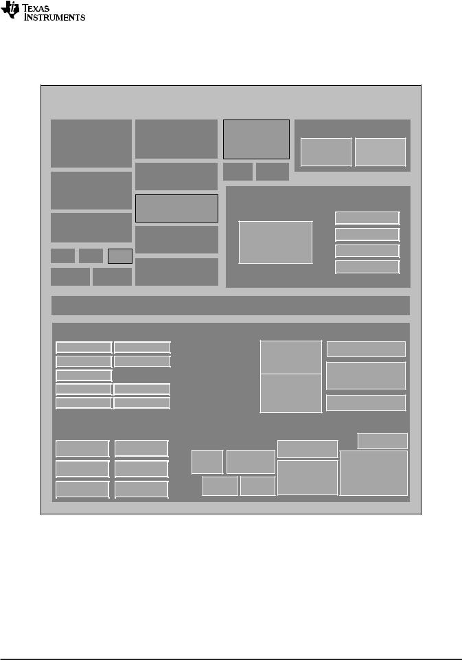
1.4Functional Block Diagram
Figure 1-1 is functional block diagram for the device.
DRA75x / DRA74x
|
|
|
MPU |
|
|
|
|
IVA HD |
|
|
|
2x EVE |
|
|
|
Radio Accelerators |
|
|
|||||||
|
(2x Arm |
|
|
|
|
1080p Video |
|
|
Analytic |
|
|
|
|
|
|
|
|
|
|||||||
|
|
|
|
|
|
|
|
|
|
|
|
|
|
|
|
||||||||||
|
|
|
|
|
Co-Processor |
|
|
|
Processors |
|
2X VCP |
|
HD ATL |
|
|
||||||||||
|
Cortex–A15) |
|
|
|
|
|
|
|
|
|
|
||||||||||||||
|
|
|
|
|
|
|
|
|
|
|
|
|
|
|
|
|
|
|
|
||||||
|
|
|
|
|
|
|
|
|
|
|
|
|
|
|
|
|
|
|
|
|
|
|
|
||
|
|
|
|
|
|
|
|
|
|
DSP1 C66x |
|
|
EDMA |
|
sDMA |
|
|
|
|
|
|
|
|
||
|
|
|
|
|
|
|
|
|
|
|
|
|
|
|
|
|
|
||||||||
|
|
|
GPU |
|
|
|
|
Co-Processors |
|
|
|
|
|
|
|
|
|
|
|
|
|
|
|||
|
|
|
|
|
|
|
|
|
|
|
|
|
|
|
|
|
|
|
|
||||||
|
(Dual-Core |
|
|
|
|
|
|
|
|
|
Display Subsystem |
|
|
||||||||||||
|
|
|
|
|
|
|
|
|
|
|
|
||||||||||||||
|
SGX544 3D) |
|
|
|
DSP2 C66x |
|
|
|
|
|
|
|
|||||||||||||
|
|
|
|
|
|
|
|
|
|
|
|
|
|
|
|
|
|
|
|||||||
|
|
|
|
|
|
|
|
|
|
Co-Processors |
|
|
|
|
|
|
|
|
|
|
|
LCD1 |
|
|
|
|
|
BB2D |
|
|
|
|
|
|
|
|
|
|
|
|
|
|
|
|
|||||||
|
|
|
|
|
|
|
|
|
|
|
|
|
|
|
|
|
|
|
|
||||||
|
|
|
|
|
|
|
|
|
|
|
|
|
|
|
|
|
|
|
|
|
|||||
|
(GC320 2D) |
|
|
|
IPU1 |
|
|
|
1XGFX / 3XVID |
|
|
|
LCD2 |
|
|
||||||||||
|
|
|
|
|
|
|
|
|
|
(Dual Cortex–M4) |
|
|
BLEND / SCALE |
|
|
|
LCD3 |
|
|
||||||
|
|
|
|
|
|
|
|
|
|
|
|
|
|
|
|
|
|||||||||
|
VIP1 |
|
VIP2 |
VIP3 |
|
|
|
|
|
|
|
|
|
|
|
|
|
|
|
||||||
|
|
|
|
|
|
|
|
|
|
|
|
|
|
|
|
|
|||||||||
|
|
|
|
|
|
|
|
|
|
IPU2 |
|
|
|
|
|
|
|
|
|
|
|
HDMI 1.4A |
|
|
|
|
2x MMU |
|
|
VPE |
|
|
|
|
|
|
|
|
|
|
|
|
|
|
|
||||||
|
|
|
|
|
(Dual Cortex–M4) |
|
|
|
|
|
|
|
|
|
|
|
|
|
|
||||||
|
|
|
|
|
|
|
|
|
|
|
|
|
|
|
|
|
|
|
|
|
|
|
|
||
|
|
|
|
|
|
|
|
|
|
|
|
|
|
|
|
|
|
|
|
|
|
|
|
|
|
|
|
|
|
|
|
|
|
|
|
|
|
|
|
|
|
|
|||||||||
|
|
|
|
|
|
|
|
|
|
High-Speed Interconnect |
|
|
|
|
|
|
|||||||||
|
|
|
|
|
|
|
|
|
|
|
|
|
|
|
|
|
|
|
|
|
|
|
|||
|
|
|
|
|
|
|
|
|
|
|
|
|
|
|
|
|
|
|
|
|
|
|
|
|
|
|
System |
|
|
|
|
|
|
|
|
|
|
|
|
Connectivity |
|
|
|||||||||
|
Spinlock |
|
Timers x16 |
|
|
|
|
|
1x USB 3.0 |
|
PCIe SS x2 |
|
|
||||||||||||
|
Mailbox x13 |
|
|
WDT |
|
|
|
|
|
|
FS/HS/SS |
|
|
|
|
|
|
||||||||
|
|
|
|
|
|
|
|
Dual Mode w/PHY |
|
|
|
|
|
||||||||||||
|
|
|
|
|
|
|
|
|
|
|
|
|
|
|
|
|
MediaLB / |
|
|
||||||
|
GPIO x8 |
|
|
|
|
|
|
|
|
|
|
|
|
|
|
|
|
|
|
||||||
|
|
|
|
|
|
|
|
|
|
|
3x USB 2.0 |
|
MOST150 |
|
|
||||||||||
|
RTC SS |
|
PWM SS x3 |
|
|
|
|
|
|
|
|
||||||||||||||
|
|
|
|
|
|
|
Dual Mode FS/HS |
|
|
|
|
|
|||||||||||||
|
HDQ |
|
|
|
KBD |
|
|
|
|
|
|
1x w/ PHY |
|
GMAC AVB |
|
|
|||||||||
|
|
|
|
|
|
|
|
|
|
2x w/ ULPI |
|
|
|
||||||||||||
|
|
|
|
|
|
|
|
|
|
|
|
|
|
|
|
|
|
|
|
|
|
|
|||
|
Serial Interfaces |
|
Program/Data Storage |
|
|
||||||||||||||||||||
|
UART X10 |
|
QSPI |
|
|
|
|
|
|
MMC / SD x4 |
|
|
DMM |
|
|
||||||||||
|
|
|
|
|
up to 2.5MiB |
|
|
|
|
|
|||||||||||||||
|
|
|
|
|
|
|
|
|
|
256KiB |
|
|
|
|
|
|
|
|
EMIF x2 |
|
|
||||
|
MCSPI X4 |
MCASP X8 |
ROM |
|
|
RAM w/ ECC GPMC / ELM |
|
|
|
|
|||||||||||||||
|
|
|
|
|
|
2x 32b |
|
|
|||||||||||||||||
|
|
|
|
|
|
|
|
|
|
|
|
|
|
|
|
|
(NAND/NOR/ |
|
|
|
|
||||
|
|
|
|
|
|
|
|
|
|
|
SATA OCMC |
|
|
|
(1) |
||||||||||
|
DCAN X2 |
|
I2C X5 |
|
Async) |
DDR2/3 w/ECC |
|||||||||||||||||||
|
|
|
|
|
|
|
|
|
|
|
|||||||||||||||
|
|
|
|
|
|
|
|
|
|
|
|
|
|
|
|
|
|
|
|
|
|
|
|
|
|
INTRO_001
Figure 1-1. DRA75x, DRA74x Block Diagram
(1) ECC is only available on EMIF1.
Copyright © 2015–2019, Texas Instruments Incorporated Device Overview 3
Submit Documentation Feedback
Product Folder Links: DRA756 DRA755 DRA754 DRA752 DRA751 DRA750 DRA746 DRA745 DRA744

DRA756, DRA755, DRA754, DRA752
DRA751, DRA750, DRA746, DRA745, DRA744
SPRS950F –DECEMBER 2015–REVISED MAY 2019 |
www.ti.com |
Table of Contents
1 |
Device Overview ......................................... |
1 |
|
|
1.1 |
Features .............................................. |
1 |
|
1.2 |
Applications........................................... |
2 |
|
1.3 |
Description............................................ |
2 |
|
1.4 |
Functional Block Diagram ........................... |
3 |
2 |
Revision History ......................................... |
5 |
|
3 |
Device Comparison ..................................... |
6 |
|
|
3.1 |
Related Products ..................................... |
9 |
4 |
Terminal Configuration and Functions ............ |
10 |
|
|
4.1 |
Terminal Assignment................................ |
10 |
|
4.2 |
Ball Characteristics.................................. |
11 |
|
4.3 |
Multiplexing Characteristics ......................... |
80 |
|
4.4 |
Signal Descriptions.................................. |
98 |
5 |
Specifications ......................................... |
140 |
|
|
5.1 |
Absolute Maximum Ratings........................ |
140 |
|
5.2 |
ESD Ratings ....................................... |
141 |
|
5.3 |
Power on Hour (POH) Limits ...................... |
142 |
|
5.4 |
Recommended Operating Conditions ............. |
143 |
|
5.5 |
Operating Performance Points..................... |
146 |
|
5.6 |
Power Consumption Summary .................... |
168 |
|
5.7 |
Electrical Characteristics........................... |
168 |
|
5.8 |
Thermal Resistance Characteristics ............... |
177 |
|
5.9 |
Power Supply Sequences ......................... |
179 |
6 |
Clock Specifications ................................. |
188 |
|
|
6.1 |
Input Clock Specifications ......................... |
189 |
|
6.2 |
RC On-die Oscillator Clock ........................ |
197 |
|
6.3 |
DPLLs, DLLs Specifications ....................... |
197 |
7 |
Timing Requirements and Switching |
|
|
|
Characteristics ........................................ |
202 |
|
|
7.1 |
Timing Test Conditions ............................ |
202 |
|
7.2 |
Interface Clock Specifications ..................... |
202 |
|
7.3 |
Timing Parameters and Information ............... |
202 |
7.4Recommended Clock and Control Signal Transition
|
Behavior............................................ |
204 |
7.5 |
Virtual and Manual I/O Timing Modes ............. |
204 |
7.6 |
Video Input Ports (VIP) ............................ |
207 |
7.7 |
Display Subsystem – Video Output Ports ......... |
225 |
7.8Display Subsystem – High-Definition Multimedia
Interface (HDMI) ................................... |
237 |
7.9 External Memory Interface (EMIF)................. |
237 |
7.10 General-Purpose Memory Controller (GPMC)..... |
237 |
7.11 |
Timers.............................................. |
259 |
7.12 |
Inter-Integrated Circuit Interface (I2C) ............. |
260 |
7.13 |
HDQ / 1-Wire Interface (HDQ1W) ................. |
263 |
7.14Universal Asynchronous Receiver Transmitter
(UART) ............................................. |
265 |
7.15Multichannel Serial Peripheral Interface (McSPI) . 266
7.16 |
Quad Serial Peripheral Interface (QSPI) .......... |
272 |
7.17 |
Multichannel Audio Serial Port (McASP) .......... |
277 |
7.18 |
Universal Serial Bus (USB) ........................ |
296 |
7.19Serial Advanced Technology Attachment (SATA). 298
7.20Peripheral Component Interconnect Express
|
(PCIe) .............................................. |
298 |
7.21 |
Controller Area Network Interface (DCAN) ........ |
299 |
7.22 |
Ethernet Interface (GMAC_SW) ................... |
299 |
7.23 |
Media Local Bus (MLB) interface .................. |
310 |
7.24 |
eMMC/SD/SDIO ................................... |
313 |
7.25 |
General-Purpose Interface (GPIO) ................ |
339 |
7.26 |
Audio Tracking Logic (ATL) ........................ |
340 |
7.27 |
System and Miscellaneous interfaces ............. |
340 |
7.28 |
Test Interfaces ..................................... |
340 |
8 Applications, Implementation, and Layout ...... |
345 |
|
8.1 |
Introduction ........................................ |
345 |
8.2 |
Power Optimizations ............................... |
346 |
8.3 |
Core Power Domains .............................. |
360 |
8.4 |
Single-Ended Interfaces ........................... |
372 |
8.5 |
Differential Interfaces .............................. |
374 |
8.6 |
Clock Routing Guidelines .......................... |
395 |
8.7DDR2/DDR3 Board Design and Layout
|
Guidelines.......................................... |
397 |
9 Device and Documentation Support.............. |
432 |
|
9.1 |
Device Nomenclature .............................. |
432 |
9.2 |
Tools and Software ................................ |
434 |
9.3 |
Documentation Support............................ |
435 |
9.4 |
Related Links ...................................... |
435 |
9.5 |
Community Resources............................. |
436 |
9.6 |
Trademarks ........................................ |
436 |
9.7 |
Electrostatic Discharge Caution ................... |
436 |
9.8 |
Glossary............................................ |
436 |
10 Mechanical, Packaging, and Orderable |
|
|
Information ............................................. |
437 |
|
10.1 |
Packaging Information ............................. |
437 |
4 |
Table of Contents |
Copyright © 2015–2019, Texas Instruments Incorporated |
Submit Documentation Feedback
Product Folder Links: DRA756 DRA755 DRA754 DRA752 DRA751 DRA750 DRA746 DRA745 DRA744

DRA756, DRA755, DRA754, DRA752
DRA751, DRA750, DRA746, DRA745, DRA744
www.ti.com SPRS950F –DECEMBER 2015–REVISED MAY 2019
2 Revision History
Changes from November 30, 2018 to May 15, 2019 (from E Revision (November 2018) to F Revision) Page
• Fixed type direction to “O” for mii1_txer and mii0_txer signals in Table 4-20, GMAC Signal Descriptions............ 122
•Added clarification notes for EMU[1:0] connections in Table 4-23, GPIOs Signal Descriptions and Table 4-27,
|
Debug Signal Descriptions ....................................................................................................... |
125 |
• Added MII_TXER timing to GMAC MII Timings section ...................................................................... |
301 |
|
• |
Updated MDIO Timing Diagram and MDIO7 parameter values ............................................................. |
303 |
• |
Added note regarding DDR ECC solutions to Table 8-43, Supported DDR3 Device Combinations ................... |
409 |
•Added clarifications about validated DDR topology in Section 8.7.3.15, CK and ADDR_CTRL Topologies and
Routing Definition .................................................................................................................. |
419 |
• Updated a note for cosmetic marks on the package.......................................................................... |
432 |
Copyright © 2015–2019, Texas Instruments Incorporated Revision History 5
Submit Documentation Feedback
Product Folder Links: DRA756 DRA755 DRA754 DRA752 DRA751 DRA750 DRA746 DRA745 DRA744

DRA756, DRA755, DRA754, DRA752
DRA751, DRA750, DRA746, DRA745, DRA744
SPRS950F –DECEMBER 2015–REVISED MAY 2019 |
www.ti.com |
3 Device Comparison
Table 3-1 shows a comparison between devices, highlighting the differences.
Table 3-1. Device Comparison(4)
|
|
|
|
|
|
DEVICE |
|
|
|
|
FEATURES |
|
|
Jacinto 6 EX |
|
|
Jacinto 6 EP |
|
|
Jacinto 6 |
|
|
|
DRA756 |
DRA755 |
DRA754 |
DRA752 |
DRA751 |
DRA750 |
DRA746 |
DRA745 |
DRA744 |
Features |
|
|
|
|
|
|
|
|
|
|
CTRL_WKUP_STD_FUSE_DIE_ID_2[31:24] Base PN register |
15 (0xF) |
14 (0xE) |
13 (0xD) |
11 (0xB) |
10 (0xA) |
9 (0x9) |
7 (0x7) |
6 (0x6) |
5 (0x5) |
|
bitfield value (3)(4) |
|
|||||||||
Processors/ Accelerators |
|
|
|
|
|
|
|
|
|
|
Speed Grades |
|
P |
L |
J |
P |
L |
J |
P |
L |
J |
Dual Arm Cortex-A15 Microprocessor |
MPU core 0 |
|
Yes |
|
|
Yes |
|
|
Yes |
|
Subsystem (MPU) |
MPU core 1 |
|
Yes |
|
|
Yes |
|
|
Yes |
|
C66x VLIW DSP |
DSP1 |
|
Yes |
|
|
Yes |
|
|
Yes |
|
DSP2 |
|
Yes |
|
|
Yes |
|
|
No |
|
|
|
|
|
|
|
|
|
||||
BitBLT 2D Hardware Acceleration Engine |
BB2D |
|
Yes |
|
|
Yes |
|
|
Yes |
|
(BB2D) |
|
|
|
|
|
|
||||
|
|
|
|
|
|
|
|
|
|
|
|
VOUT1 |
|
Yes |
|
|
Yes |
|
|
Yes |
|
Display Subsystem |
VOUT2 |
|
Yes |
|
|
Yes |
|
|
Yes |
|
VOUT3 |
|
Yes |
|
|
Yes |
|
|
Yes |
|
|
|
|
|
|
|
|
|
||||
|
HDMI |
|
Yes |
|
|
Yes |
|
|
Yes |
|
Embedded Vision Engine (EVE) |
EVE1 |
|
Yes |
|
|
No |
|
|
No |
|
EVE2 |
|
Yes |
|
|
No |
|
|
No |
|
|
|
|
|
|
|
|
|
||||
Dual Arm Cortex-M4 Image Processing Unit |
IPU1 |
|
Yes |
|
|
Yes |
|
|
Yes |
|
(IPU) |
IPU2 |
|
Yes |
|
|
Yes |
|
|
Yes |
|
Image Video Accelarator (IVA) |
IVA |
|
Yes |
|
|
Yes |
|
|
Yes |
|
SGX544 Dual-Core 3D Graphics Processing |
GPU |
|
Yes |
|
|
Yes |
|
|
Yes |
|
Unit (GPU) |
|
|
|
|
|
|
||||
|
|
|
|
|
|
|
|
|
|
|
6 Device Comparison Copyright © 2015–2019, Texas Instruments Incorporated
Submit Documentation Feedback
Product Folder Links: DRA756 DRA755 DRA754 DRA752 DRA751 DRA750 DRA746 DRA745 DRA744

DRA756, DRA755, DRA754, DRA752
DRA751, DRA750, DRA746, DRA745, DRA744
www.ti.com SPRS950F –DECEMBER 2015 –REVISED MAY 2019
Table 3-1. Device Comparison(4) (continued)
|
|
|
|
|
|
|
DEVICE |
|
|
|
|
|
FEATURES |
|
|
Jacinto 6 EX |
|
|
Jacinto 6 EP |
|
|
Jacinto 6 |
|
||
|
|
|
DRA756 |
DRA755 |
DRA754 |
DRA752 |
DRA751 |
DRA750 |
DRA746 |
DRA745 |
DRA744 |
|
|
|
vin1a |
|
Yes |
|
|
Yes |
|
|
No |
|
|
|
VIP1 |
vin1b |
|
Yes |
|
|
Yes |
|
|
No |
|
|
|
vin2a |
|
Yes |
|
|
Yes |
|
|
Yes |
|
||
|
|
|
|
|
|
|
|
|||||
|
|
vin2b |
|
Yes |
|
|
Yes |
|
|
Yes |
|
|
Video Input Port (VIP) |
|
vin3a |
|
Yes |
|
|
Yes |
|
|
Yes |
|
|
VIP2 |
vin3b |
|
Yes |
|
|
Yes |
|
|
Yes |
|
||
|
|
|
|
|
|
|
||||||
|
vin4a |
|
Yes |
|
|
Yes |
|
|
Yes |
|
||
|
|
|
|
|
|
|
|
|||||
|
|
vin4b |
|
Yes |
|
|
Yes |
|
|
Yes |
|
|
|
VIP3 |
vin5a |
|
Yes |
|
|
Yes |
|
|
No |
|
|
|
vin6a |
|
Yes |
|
|
Yes |
|
|
No |
|
||
|
|
|
|
|
|
|
|
|||||
Video Processing Engine (VPE) |
VPE |
|
Yes |
|
|
Yes |
|
|
Yes |
|
||
Program/Data Storage |
|
|
|
|
|
|
|
|
|
|
||
|
|
OCMC_RAM1 |
|
512KB |
|
|
512KB |
|
|
512KB |
|
|
On-Chip Shared Memory (RAM) |
OCMC_RAM2 |
|
1MB |
|
|
No |
|
|
No |
|
||
|
|
OCMC_RAM3 |
|
1MB |
|
|
No |
|
|
No |
|
|
General-Purpose Memory Controller (GPMC) |
GPMC |
|
Yes |
|
|
Yes |
|
|
Yes |
|
||
DDR2/DDR3 Memory Controller (2) |
EMIF1 |
up to 2GB (with optional SECDED) |
up to 2GB (with optional SECDED) |
|
up to 2GB |
|
||||||
EMIF2 |
|
up to 2GB |
|
|
up to 2GB |
|
|
up to 2GB |
|
|||
|
|
|
|
|
|
|
|
|||||
Dynamic Memory Manager (DMM) |
DMM |
|
Yes |
|
|
Yes |
|
|
Yes |
|
||
Radio Support |
|
|
|
|
|
|
|
|
|
|
||
Audio Tracking Logic (ATL) |
ATL |
|
Yes |
|
|
Yes |
|
|
Yes |
|
||
Viterbi Coprocessor (VCP) |
VCP1 |
|
Yes |
|
|
Yes |
|
|
Yes |
|
||
VCP2 |
|
Yes |
|
|
Yes |
|
|
Yes |
|
|||
|
|
|
|
|
|
|
|
|||||
Peripherals |
|
|
|
|
|
|
|
|
|
|
||
Dual Controller Area Network Interface (DCAN) |
DCAN1 |
|
Yes |
|
|
Yes |
|
|
Yes |
|
||
DCAN2 |
|
Yes |
|
|
Yes |
|
|
Yes |
|
|||
|
|
|
|
|
|
|
|
|||||
Enhanced DMA (EDMA) |
EDMA |
|
Yes |
|
|
Yes |
|
|
Yes |
|
||
System DMA (DMA_SYSTEM) |
DMA_SYSTEM |
|
Yes |
|
|
Yes |
|
|
Yes |
|
||
Ethernet Subsystem (Ethernet SS) |
GMAC_SW[0] |
MII, RMII, or RGMII |
MII, RMII, or RGMII |
MII, RMII, or RGMII |
||||||||
GMAC_SW[1] |
MII, RMII, or RGMII |
MII, RMII, or RGMII |
MII, RMII, or RGMII |
|||||||||
|
|
|||||||||||
General-Purpose I/O (GPIO) |
GPIO |
|
up to 247 |
|
|
up to 247 |
|
|
up to 247 |
|
||
Copyright © 2015–2019, Texas Instruments Incorporated Device Comparison 7
Submit Documentation Feedback
Product Folder Links: DRA756 DRA755 DRA754 DRA752 DRA751 DRA750 DRA746 DRA745 DRA744

DRA756, DRA755, DRA754, DRA752
DRA751, DRA750, DRA746, DRA745, DRA744
SPRS950F –DECEMBER 2015–REVISED MAY 2019 www.ti.com
Table 3-1. Device Comparison(4) (continued)
|
|
|
|
|
|
|
|
|
DEVICE |
|
|
|
|
|
FEATURES |
|
|
Jacinto 6 EX |
|
|
|
|
Jacinto 6 EP |
|
|
Jacinto 6 |
|
|
|
|
DRA756 |
DRA755 |
|
DRA754 |
|
DRA752 |
DRA751 |
DRA750 |
DRA746 |
DRA745 |
DRA744 |
Inter-Integrated Circuit Interface (I2C) |
I2C |
|
5 |
|
|
|
|
5 |
|
|
5 |
|
|
System Mailbox Module |
MAILBOX |
|
13 |
|
|
|
|
13 |
|
|
13 |
|
|
Media Local Bus Subsystem (MLBSS) |
MLB |
|
Yes |
|
|
|
Yes |
|
|
Yes |
|
||
|
|
McASP1 |
|
16 serializers |
|
|
|
16 serializers |
|
|
16 serializers |
|
|
|
|
McASP2 |
|
16 serializers |
|
|
|
16 serializers |
|
|
16 serializers |
|
|
|
|
McASP3 |
|
4 serializers |
|
|
|
4 serializers |
|
|
4 serializers |
|
|
Multichannel Audio Serial Port (McASP) |
McASP4 |
|
4 serializers |
|
|
|
4 serializers |
|
|
4 serializers |
|
||
McASP5 |
|
4 serializers |
|
|
|
4 serializers |
|
|
4 serializers |
|
|||
|
|
|
|
|
|
|
|
|
|||||
|
|
McASP6 |
|
4 serializers |
|
|
|
4 serializers |
|
|
4 serializers |
|
|
|
|
McASP7 |
|
4 serializers |
|
|
|
4 serializers |
|
|
4 serializers |
|
|
|
|
McASP8 |
|
4 serializers |
|
|
|
4 serializers |
|
|
4 serializers |
|
|
|
|
MMC1 |
|
1x UHSI 4b |
|
|
|
1x UHSI 4b |
|
|
1x UHSI 4b |
|
|
MultiMedia Card/Secure Digital/Secure Digital |
MMC2 |
|
1x eMMC™ 8b |
|
|
|
1x eMMC 8b |
|
|
1x eMMC 8b |
|
||
Input Output Interface (MMC/SD/SDIO) |
MMC3 |
|
1x SDIO 8b |
|
|
|
1x SDIO 8b |
|
|
1x SDIO 8b |
|
||
|
|
MMC4 |
|
1x SDIO 4b |
|
|
|
1x SDIO 4b |
|
|
1x SDIO 4b |
|
|
PCI Express 3.0 Port with Integrated PHY |
PCIe_SS1 |
|
Yes |
|
|
|
Yes |
|
Yes (Single-lane mode) |
||||
PCIe_SS2 |
|
Yes |
|
|
|
Yes |
|
|
No |
|
|||
|
|
|
|
|
|
|
|
|
|||||
SATA |
|
SATA |
|
Yes |
|
|
|
Yes |
|
|
Yes |
|
|
Real-Time Clock Subsystem (RTCSS) |
RTCSS |
|
Yes |
|
|
|
Yes |
|
|
Yes |
|
||
Multichannel Serial Peripheral Interface (McSPI) |
McSPI |
|
4 |
|
|
|
|
4 |
|
|
4 |
|
|
HDQ1W |
HDQ1W |
|
Yes |
|
|
|
Yes |
|
|
Yes |
|
||
Quad SPI (QSPI) |
QSPI |
|
Yes |
|
|
|
Yes |
|
|
Yes |
|
||
Spinlock Module |
SPINLOCK |
|
Yes |
|
|
|
Yes |
|
|
Yes |
|
||
Keyboard Controller (KBD) |
KBD |
|
Yes |
|
|
|
Yes |
|
|
Yes |
|
||
Timers, General-Purpose |
TIMER |
|
16 |
|
|
|
|
16 |
|
|
16 |
|
|
Timer, Watchdog |
WATCHDOG |
|
Yes |
|
|
|
Yes |
|
|
Yes |
|
||
TIMER |
|
|
|
|
|
|
|
||||||
|
|
|
|
|
|
|
|
|
|
|
|
|
|
|
|
PWMSS1 |
|
Yes |
|
|
|
Yes |
|
|
Yes |
|
|
Pulse-Width Modulation Subsystem (PWMSS) |
PWMSS2 |
|
Yes |
|
|
|
Yes |
|
|
Yes |
|
||
|
|
PWMSS3 |
|
Yes |
|
|
|
Yes |
|
|
Yes |
|
|
Universal Asynchronous Receiver/Transmitter |
UART |
|
10 |
|
|
|
|
10 |
|
|
10 |
|
|
(UART) |
|
|
|
|
|
|
|
|
|
||||
|
|
|
|
|
|
|
|
|
|
|
|
|
|
|
|
|
|
|
|
|
|
|
|
|
|
|
|
8 |
Device Comparison |
|
|
|
|
|
|
|
|
Copyright © 2015–2019, Texas Instruments Incorporated |
|||
|
|
|
Submit Documentation Feedback |
|
|
|
|
|
|
||||
|
Product Folder Links: DRA756 DRA755 DRA754 DRA752 DRA751 DRA750 DRA746 DRA745 DRA744 |
|
|
|
|||||||||

DRA756, DRA755, DRA754, DRA752
DRA751, DRA750, DRA746, DRA745, DRA744
www.ti.com SPRS950F –DECEMBER 2015 –REVISED MAY 2019
Table 3-1. Device Comparison(4) (continued)
|
|
|
|
|
|
DEVICE |
|
|
|
|
FEATURES |
|
|
Jacinto 6 EX |
|
|
Jacinto 6 EP |
|
|
Jacinto 6 |
|
|
|
DRA756 |
DRA755 |
DRA754 |
DRA752 |
DRA751 |
DRA750 |
DRA746 |
DRA745 |
DRA744 |
|
USB1 |
|
|
|
|
|
|
|
|
|
Universal Serial Bus (USB3.0) |
(SuperSpeed, |
|
Yes |
|
|
Yes |
|
|
Yes |
|
Dual-Role-Device |
|
|
|
|
|
|
||||
|
|
|
|
|
|
|
|
|
|
|
|
[DRD]) |
|
|
|
|
|
|
|
|
|
|
USB2 (HighSpeed, |
|
|
|
|
|
|
|
|
|
|
Dual-Role-Device |
|
|
|
|
|
|
|
|
|
|
[DRD], with |
|
Yes |
|
|
Yes |
|
|
Yes |
|
|
embedded HS |
|
|
|
|
|
|
|
|
|
|
PHY) |
|
|
|
|
|
|
|
|
|
Universal Serial Bus (USB2.0) |
USB3 (HighSpeed, |
|
|
|
|
|
|
|
|
|
|
OTG2.0, with |
|
Yes |
|
|
Yes |
|
|
Yes |
|
|
ULPI) |
|
|
|
|
|
|
|
|
|
|
USB4 (HighSpeed, |
|
|
|
|
|
|
|
Yes(1) |
|
|
OTG2.0, with |
|
Yes |
|
|
Yes |
|
|
|
|
|
ULPI) |
|
|
|
|
|
|
|
|
|
(1)USB4 will not be supported on some pin-compatible roadmap devices. USB3 will be mapped to these balls instead. Pin compatibility can be maintained in the future by either not using USB4, or via software change to use USB4 on this device, but USB3 on these balls in the future.
(2)In the Unified L3 memory map, there is maximum of 2GB of SDRAM space which is available to all L3 initiators including MPU (MPU, GPU, DSP, IVA, DMA, etc). Typically this space is interleaved across both EMIFs to optimize memory performance. If a system populates > 2GB of physical memory, that additional addressable space can be accessed only by the MPU via the Arm V7 Large Physical Address Extensions (LPAE).
(3)For more details about the CTRL_WKUP_STD_FUSE_DIE_ID_2 register and Base PN bitfield, see the DRA75x, DRA74x SoC for Automotive Infotainment Silicon Revision 2.0, 1.x.
(4)X5777x is the base part number for the superset device. Software should constrain the features used to match the intended production device. The Base PN register bitfield value is 0x3F.
3.1Related Products
Automotive Processors
DRAx Infotainment SoCs The "Jacinto 6" family of infotainment processors (DRA7xx), paired with robust software and ecosystem offering bring unprecedented feature-rich, in-vehicle infotainment, instrument cluster and telematics features to the next generation automobiles.
Copyright © 2015–2019, Texas Instruments Incorporated Device Comparison 9
Submit Documentation Feedback
Product Folder Links: DRA756 DRA755 DRA754 DRA752 DRA751 DRA750 DRA746 DRA745 DRA744

DRA756, DRA755, DRA754, DRA752
DRA751, DRA750, DRA746, DRA745, DRA744
SPRS950F –DECEMBER 2015–REVISED MAY 2019 |
www.ti.com |
4 Terminal Configuration and Functions
4.1Terminal Assignment
Figure 4-1 shows the ball locations for the 760 plastic ball grid array (PBGA) package and are used in conjunction with Table 4-2 through Table 4-34 to locate signal names and ball grid numbers.
Figure 4-1. ABC S-PBGA-N760 Package (Bottom View)
NOTE
The following bottom balls are not connected: AF7 / AF10 / AF13 / AF16 / AF19 / AE4 /
AE25 / AB26 / W3 / W26 / T3 / T26 / N3 / N26 / K3 / K26 / G3 / D4 / D25 / C10 / C13 / C16 /
C19 / C22.
These balls do not exist on the package.
4.1.1Unused Balls Connection Requirements
This section describes the Unused/Reserved balls connection requirements.
NOTE
The following balls are reserved: A27 / K14 / Y5 / Y10 / B28
These balls must be left unconnected.
NOTE
All unused power supply balls must be supplied with the voltages specified in the Section 5.4, Recommended Operating Conditions, unless alternative tie-off options are included in Section 4.4, Signal Descriptions.
Table 4-1. Unused Balls Specific Connection Requirements
|
BALLS |
CONNECTION REQUIREMENTS |
|
AE15 / AC15 / AE14 / D20 / AD17 / AC17 / AC16 / AB16 / V27 / |
These balls must be connected to GND through an external pull |
|
AH25 / AE27 / AD27 / Y28 / G28 / H27 / K27 / M28 |
resistor if unused |
E20 / D21 / E23 / C20 / C21 / V28 / F18 / AG25 / AE28 / AD28 / Y27 |
These balls must be connected to the corresponding power supply |
|
|
/ G27 / H28 / K28 / M27 / F17 / C25 |
through an external pull resistor if unused |
|
|
|
10 |
Terminal Configuration and Functions |
Copyright © 2015–2019, Texas Instruments Incorporated |
Submit Documentation Feedback
Product Folder Links: DRA756 DRA755 DRA754 DRA752 DRA751 DRA750 DRA746 DRA745 DRA744
|
DRA756, DRA755, DRA754, DRA752 |
|
DRA751, DRA750, DRA746, DRA745, DRA744 |
www.ti.com |
SPRS950F –DECEMBER 2015–REVISED MAY 2019 |
Table 4-1. Unused Balls Specific Connection Requirements (continued) |
|
|
|
BALLS |
CONNECTION REQUIREMENTS |
This ball should be connected to the corresponding power supply AF14 (rtc_iso) through an external pull resistor if unused; or can be connected to
F22 (porz) when RTC unused (level translation may be needed)
This ball should be connected to VSS when RTC is unused; or can AB17 (rtc_porz) be connected to F22 (porz) when RTC unused (level translation may
be needed)
NOTE
All other unused signal balls with a Pad Configuration Register can be left unconnected with their internal pullup or pulldown resistor enabled.
NOTE
All other unused signal balls without Pad Configuration Register can be left unconnected.
4.2Ball Characteristics
Table 4-2 describes the terminal characteristics and the signals multiplexed on each ball. The following list describes the table column headers:
1.BALL NUMBER: Ball number(s) on the bottom side associated with each signal on the bottom.
2.BALL NAME: Mechanical name from package device (name is taken from muxmode 0).
3.SIGNAL NAME: Names of signals multiplexed on each ball (also notice that the name of the ball is the signal name in muxmode 0).
NOTE
Table 4-2 does not take into account the subsystem multiplexing signals. Subsystem multiplexing signals are described in Section 4.4, Signal Descriptions.
NOTE
In the Driver off mode, the buffer is configured in high-impedance.
4.74x: This column shows if the functionality is applicable for DRA74x devices. Note that the ball characteristics table presents the functionality of DRA75x device. An empty box means "Yes".
5.MUXMODE: Multiplexing mode number:
a.MUXMODE 0 is the primary mode; this means that when MUXMODE=0 is set, the function mapped on the pin corresponds to the name of the pin. The primary muxmode is not necessarily the default muxmode.
NOTE
The default mode is the mode at the release of the reset; also see the RESET REL.
MUXMODE column.
b.MUXMODE 1 through 15 are possible muxmodes for alternate functions. On each pin, some muxmodes are effectively used for alternate functions, while some muxmodes are not used. Only MUXMODE values which correspond to defined functions should be used.
c.An empty box means Not Applicable.
6.TYPE: Signal type and direction:
–I = Input
Copyright © 2015–2019, Texas Instruments Incorporated |
Terminal Configuration and Functions |
11 |
Submit Documentation Feedback
Product Folder Links: DRA756 DRA755 DRA754 DRA752 DRA751 DRA750 DRA746 DRA745 DRA744

DRA756, DRA755, DRA754, DRA752
DRA751, DRA750, DRA746, DRA745, DRA744
SPRS950F –DECEMBER 2015–REVISED MAY 2019 |
www.ti.com |
–O = Output
–IO = Input or Output
–D = Open drain
–DS = Differential Signaling
–A = Analog
–PWR = Power
–GND = Ground
–CAP = LDO Capacitor
7.BALL RESET STATE: The state of the terminal at power-on reset:
–drive 0 (OFF): The buffer drives VOL (pulldown or pullup resistor not activated)
–drive 1 (OFF): The buffer drives VOH (pulldown or pullup resistor not activated)
–OFF: High-impedance
–PD: High-impedance with an active pulldown resistor
–PU: High-impedance with an active pullup resistor
–An empty box means Not Applicable
8.BALL RESET REL. STATE: The state of the terminal at the deactivation of the rstoutn signal (also mapped to the PRCM SYS_WARM_OUT_RST signal)
–drive 0 (OFF): The buffer drives VOL (pulldown or pullup resistor not activated)
–drive clk (OFF): The buffer drives a toggling clock (pulldown or pullup resistor not activated)
–drive 1 (OFF): The buffer drives VOH (pulldown or pullup resistor not activated)
–OFF: High-impedance
–PD: High-impedance with an active pulldown resistor
–PU: High-impedance with an active pullup resistor
–An empty box means Not Applicable
NOTE
For more information on the CORE_PWRON_RET_RST reset signal and its reset sources, see the Power Reset and Clock Management / PRCM Reset Management Functional Description section of the Device TRM.
9.BALL RESET REL. MUXMODE: This muxmode is automatically configured at the release of the rstoutn signal (also mapped to the PRCM SYS_WARM_OUT_RST signal).
An empty box means Not Applicable.
10.IO VOLTAGE VALUE: This column describes the IO voltage value (VDDS supply).
An empty box means Not Applicable.
11.POWER: The voltage supply that powers the terminal IO buffers. An empty box means Not Applicable.
12.HYS: Indicates if the input buffer is with hysteresis:
–Yes: With hysteresis
–No: Without hysteresis
–An empty box: Not Applicable
NOTE
For more information, see the hysteresis values in Section 5.7, Electrical Characteristics.
13. BUFFER TYPE: Drive strength of the associated output buffer.
An empty box means Not Applicable.
12 |
Terminal Configuration and Functions |
Copyright © 2015–2019, Texas Instruments Incorporated |
Submit Documentation Feedback
Product Folder Links: DRA756 DRA755 DRA754 DRA752 DRA751 DRA750 DRA746 DRA745 DRA744
DRA756, DRA755, DRA754, DRA752
DRA751, DRA750, DRA746, DRA745, DRA744
www.ti.com |
SPRS950F –DECEMBER 2015–REVISED MAY 2019 |
|
|
|
|
NOTE
For programmable buffer strength:
–The default value is given in Table 4-2.
–A note describes all possible values according to the selected muxmode.
14.PULLUP / PULLDOWN TYPE: Denotes the presence of an internal pullup or pulldown resistor. Pullup and pulldown resistors can be enabled or disabled via software.
–PU: Internal pullup
–PD: Internal pulldown
–PU/PD: Internal pullup and pulldown
–PUx/PDy: Programmable internal pullup and pulldown
–PDy: Programmable internal pulldown
–An empty box means No pull
15.DSIS: The deselected input state (DSIS) indicates the state driven on the peripheral input (logic "0" or logic "1") when the peripheral pin function is not selected by any of the PINCNTLx registers.
–0: Logic 0 driven on the peripheral's input signal port.
–1: Logic 1 driven on the peripheral's input signal port.
–blank: Pin state driven on the peripheral's input signal port.
NOTE
Configuring two pins to the same input signal is not supported as it can yield unexpected results. This can be easily prevented with the proper software configuration. (Hi-Z mode is not an input signal.)
NOTE
When a pad is set into a multiplexing mode which is not defined by pin multiplexing, that pad’s behavior is undefined. This should be avoided.
CAUTION
Peripherals exposed in Ball Characteristics Table and Multiplexing Characteristics Table represent functionality of a DRA75x device. Not all exposed peripherals are supported on DRA7xx devices. For peripherals supported on DRA7xx family of products please refer to Table 3-1, Device Comparison.
NOTE
Some of the DDR1 and DDR2 signals have an additional state change at the release of porz.
The state that the signals change to at the release of porz is as follows:
drive 0 (OFF) for: ddr1_csn0, ddr1_ck, ddr1_nck, ddr1_nck, ddr1_casn, ddr1_rasn, ddr1_wen, ddr1_ba[2:0], ddr1_a[15:0], ddr2_csn0, ddr2_ck, ddr2_nck, ddr2_casn, ddr2_rasn, ddr2_wen, ddr2_ba[2:0], ddr2_a[15:0].
OFF for: ddr1_ecc_d[7:0], ddr1_dqm[3:0], ddr1_dqm_ecc, ddr1_dqs[3:0], ddr1_dqsn[3:0], ddr1_dqs_ecc, ddr1_dqsn_ecc, ddr1_d[31:0], ddr2_dqm[3:0], ddr2_dqs[3:0], ddr2_dqsn[3:0], ddr2_d[31:0].
Copyright © 2015–2019, Texas Instruments Incorporated |
Terminal Configuration and Functions |
13 |
Submit Documentation Feedback
Product Folder Links: DRA756 DRA755 DRA754 DRA752 DRA751 DRA750 DRA746 DRA745 DRA744

DRA756, DRA755, DRA754, DRA752
DRA751, DRA750, DRA746, DRA745, DRA744
SPRS950F –DECEMBER 2015–REVISED MAY 2019 |
www.ti.com |
Table 4-2. Ball Characteristics(1)
|
|
|
|
|
|
|
BALL |
BALL |
|
|
|
|
|
|
|
|
|
|
|
|
|
BALL |
RESET |
I/O |
|
|
|
PULL |
|
||
|
|
|
|
MUXMODE |
|
RESET |
POWER |
|
BUFFER |
|
|||||
BALL NUMBER [1] |
BALL NAME [2] |
SIGNAL NAME [3] |
74x [4] |
TYPE [6] |
RESET |
REL. |
VOLTAGE |
HYS [12] |
UP/DOWN |
DSIS [15] |
|||||
[5] |
REL. |
[11] |
TYPE [13] |
||||||||||||
|
|
|
|
|
|
STATE [7] |
STATE [8] |
MUXMODE |
VALUE [10] |
|
|
|
TYPE [14] |
|
|
|
|
|
|
|
|
|
|
[9] |
|
|
|
|
|
|
|
K9 |
cap_vbbldo_dspeve |
cap_vbbldo_dspeve |
|
|
CAP |
|
|
|
|
|
|
|
|
|
|
|
|
|
|
|
|
|
|
|
|
|
|
|
|
|
|
Y14 |
cap_vbbldo_gpu |
cap_vbbldo_gpu |
|
|
CAP |
|
|
|
|
|
|
|
|
|
|
|
|
|
|
|
|
|
|
|
|
|
|
|
|
|
|
R20 |
cap_vbbldo_iva |
cap_vbbldo_iva |
|
|
CAP |
|
|
|
|
|
|
|
|
|
|
|
|
|
|
|
|
|
|
|
|
|
|
|
|
|
|
J16 |
cap_vbbldo_mpu |
cap_vbbldo_mpu |
|
|
CAP |
|
|
|
|
|
|
|
|
|
|
|
|
|
|
|
|
|
|
|
|
|
|
|
|
|
|
L9 |
cap_vddram_core1 |
cap_vddram_core1 |
|
|
CAP |
|
|
|
|
|
|
|
|
|
|
|
|
|
|
|
|
|
|
|
|
|
|
|
|
|
|
J19 |
cap_vddram_core2 |
cap_vddram_core2 |
|
|
CAP |
|
|
|
|
|
|
|
|
|
|
|
|
|
|
|
|
|
|
|
|
|
|
|
|
|
|
Y15 |
cap_vddram_core3 |
cap_vddram_core3 |
|
|
CAP |
|
|
|
|
|
|
|
|
|
|
|
|
|
|
|
|
|
|
|
|
|
|
|
|
|
|
P19 |
cap_vddram_core4 |
cap_vddram_core4 |
|
|
CAP |
|
|
|
|
|
|
|
|
|
|
|
|
|
|
|
|
|
|
|
|
|
|
|
|
|
|
Y16 |
cap_vddram_core5 |
cap_vddram_core5 |
|
|
CAP |
|
|
|
|
|
|
|
|
|
|
|
|
|
|
|
|
|
|
|
|
|
|
|
|
|
|
J10 |
cap_vddram_dspeve1 |
cap_vddram_dspeve1 |
|
|
CAP |
|
|
|
|
|
|
|
|
|
|
|
|
|
|
|
|
|
|
|
|
|
|
|
|
|
|
J9 |
cap_vddram_dspeve2 |
cap_vddram_dspeve2 |
|
|
CAP |
|
|
|
|
|
|
|
|
|
|
|
|
|
|
|
|
|
|
|
|
|
|
|
|
|
|
Y13 |
cap_vddram_gpu |
cap_vddram_gpu |
|
|
CAP |
|
|
|
|
|
|
|
|
|
|
|
|
|
|
|
|
|
|
|
|
|
|
|
|
|
|
T20 |
cap_vddram_iva |
cap_vddram_iva |
|
|
CAP |
|
|
|
|
|
|
|
|
|
|
|
|
|
|
|
|
|
|
|
|
|
|
|
|
|
|
K16 |
cap_vddram_mpu1 |
cap_vddram_mpu1 |
|
|
CAP |
|
|
|
|
|
|
|
|
|
|
|
|
|
|
|
|
|
|
|
|
|
|
|
|
|
|
K19 |
cap_vddram_mpu2 |
cap_vddram_mpu2 |
|
|
CAP |
|
|
|
|
|
|
|
|
|
|
|
|
|
|
|
|
|
|
|
|
|
|
|
|
|
|
G19 |
dcan1_rx |
dcan1_rx |
|
0 |
IO |
PU |
PU |
15 |
1.8/3.3 |
vddshv3 |
Yes |
Dual |
PU/PD |
1 |
|
|
|
|
|
|
|
|
|
|
|
|
|
Voltage |
|
|
|
|
|
uart8_txd |
|
2 |
O |
|
|
|
|
|
|
|
|
||
|
|
|
|
|
|
|
|
|
LVCMOS |
|
|
||||
|
|
|
|
|
|
|
|
|
|
|
|
|
|
||
|
|
mmc2_sdwp |
|
3 |
I |
|
|
|
|
|
|
|
|
0 |
|
|
|
|
|
|
|
|
|
|
|
|
|
|
|
|
|
|
|
sata1_led |
|
4 |
O |
|
|
|
|
|
|
|
|
|
|
|
|
|
|
|
|
|
|
|
|
|
|
|
|
|
|
|
|
hdmi1_cec |
|
6 |
IO |
|
|
|
|
|
|
|
|
|
|
|
|
|
|
|
|
|
|
|
|
|
|
|
|
|
|
|
|
gpio1_15 |
|
14 |
IO |
|
|
|
|
|
|
|
|
|
|
|
|
|
|
|
|
|
|
|
|
|
|
|
|
|
|
|
|
Driver off |
|
15 |
I |
|
|
|
|
|
|
|
|
|
|
|
|
|
|
|
|
|
|
|
|
|
|
|
|
|
|
G20 |
dcan1_tx |
dcan1_tx |
|
0 |
IO |
PU |
PU |
15 |
1.8/3.3 |
vddshv3 |
Yes |
Dual |
PU/PD |
1 |
|
|
|
|
|
|
|
|
|
|
|
|
|
Voltage |
|
|
|
|
|
uart8_rxd |
|
2 |
I |
|
|
|
|
|
|
|
1 |
||
|
|
|
|
|
|
|
|
|
LVCMOS |
|
|||||
|
|
|
|
|
|
|
|
|
|
|
|
|
|
||
|
|
mmc2_sdcd |
|
3 |
I |
|
|
|
|
|
|
|
|
1 |
|
|
|
|
|
|
|
|
|
|
|
|
|
|
|
|
|
|
|
hdmi1_hpd |
|
6 |
I |
|
|
|
|
|
|
|
|
|
|
|
|
|
|
|
|
|
|
|
|
|
|
|
|
|
|
|
|
gpio1_14 |
|
14 |
IO |
|
|
|
|
|
|
|
|
|
|
|
|
|
|
|
|
|
|
|
|
|
|
|
|
|
|
|
|
Driver off |
|
15 |
I |
|
|
|
|
|
|
|
|
|
|
|
|
|
|
|
|
|
|
|
|
|
|
|
|
|
|
AD20 |
ddr1_a0 |
ddr1_a0 |
|
0 |
O |
PD |
drive 1 |
|
1.35/1.5/1.8 |
vdds_ddr1 |
No |
LVCMOS |
Pux/PDy |
|
|
|
|
|
|
|
|
|
(OFF) |
|
|
|
|
DDR |
|
|
|
AC19 |
ddr1_a1 |
ddr1_a1 |
|
0 |
O |
PD |
drive 1 |
|
1.35/1.5/1.8 |
vdds_ddr1 |
No |
LVCMOS |
Pux/PDy |
|
|
|
|
|
|
|
|
|
(OFF) |
|
|
|
|
DDR |
|
|
|
|
|
|
|
|
|
|
|
|
|
|
|
|
|
|
|
AD21 |
ddr1_a10 |
ddr1_a10 |
|
0 |
O |
PD |
drive 1 |
|
1.35/1.5/1.8 |
vdds_ddr1 |
No |
LVCMOS |
Pux/PDy |
|
|
|
|
|
|
|
|
|
(OFF) |
|
|
|
|
DDR |
|
|
|
|
|
|
|
|
|
|
|
|
|
|
|
|
|
|
|
AD22 |
ddr1_a11 |
ddr1_a11 |
|
0 |
O |
PD |
drive 1 |
|
1.35/1.5/1.8 |
vdds_ddr1 |
No |
LVCMOS |
Pux/PDy |
|
|
|
|
|
|
|
|
|
(OFF) |
|
|
|
|
DDR |
|
|
|
AC21 |
ddr1_a12 |
ddr1_a12 |
|
0 |
O |
PD |
drive 1 |
|
1.35/1.5/1.8 |
vdds_ddr1 |
No |
LVCMOS |
Pux/PDy |
|
|
|
|
|
|
|
|
|
(OFF) |
|
|
|
|
DDR |
|
|
|
|
|
|
|
|
|
|
|
|
|
|
|
|
|
|
14 |
Terminal Configuration and Functions |
Copyright © 2015–2019, Texas Instruments Incorporated |
Submit Documentation Feedback
Product Folder Links: DRA756 DRA755 DRA754 DRA752 DRA751 DRA750 DRA746 DRA745 DRA744

DRA756, DRA755, DRA754, DRA752
DRA751, DRA750, DRA746, DRA745, DRA744
www.ti.com |
SPRS950F –DECEMBER 2015 –REVISED MAY 2019 |
Table 4-2. Ball Characteristics(1) (continued)
|
|
|
|
|
|
|
BALL |
BALL |
|
|
|
|
|
|
|
|
|
|
|
|
|
BALL |
RESET |
I/O |
|
|
|
PULL |
|
||
|
|
|
|
MUXMODE |
|
RESET |
POWER |
|
BUFFER |
|
|||||
BALL NUMBER [1] |
BALL NAME [2] |
SIGNAL NAME [3] |
74x [4] |
TYPE [6] |
RESET |
REL. |
VOLTAGE |
HYS [12] |
UP/DOWN |
DSIS [15] |
|||||
[5] |
REL. |
[11] |
TYPE [13] |
||||||||||||
|
|
|
|
|
|
STATE [7] |
STATE [8] |
MUXMODE |
VALUE [10] |
|
|
|
TYPE [14] |
|
|
|
|
|
|
|
|
|
|
[9] |
|
|
|
|
|
|
|
AF18 |
ddr1_a13 |
ddr1_a13 |
|
0 |
O |
PD |
drive 1 |
|
1.35/1.5/1.8 |
vdds_ddr1 |
No |
LVCMOS |
Pux/PDy |
|
|
|
|
|
|
|
|
|
(OFF) |
|
|
|
|
DDR |
|
|
|
|
|
|
|
|
|
|
|
|
|
|
|
|
|
|
|
AE17 |
ddr1_a14 |
ddr1_a14 |
|
0 |
O |
PD |
drive 1 |
|
1.35/1.5/1.8 |
vdds_ddr1 |
No |
LVCMOS |
Pux/PDy |
|
|
|
|
|
|
|
|
|
(OFF) |
|
|
|
|
DDR |
|
|
|
|
|
|
|
|
|
|
|
|
|
|
|
|
|
|
|
AD18 |
ddr1_a15 |
ddr1_a15 |
|
0 |
O |
PD |
drive 1 |
|
1.35/1.5/1.8 |
vdds_ddr1 |
No |
LVCMOS |
Pux/PDy |
|
|
|
|
|
|
|
|
|
(OFF) |
|
|
|
|
DDR |
|
|
|
AC20 |
ddr1_a2 |
ddr1_a2 |
|
0 |
O |
PD |
drive 1 |
|
1.35/1.5/1.8 |
vdds_ddr1 |
No |
LVCMOS |
Pux/PDy |
|
|
|
|
|
|
|
|
|
(OFF) |
|
|
|
|
DDR |
|
|
|
AB19 |
ddr1_a3 |
ddr1_a3 |
|
0 |
O |
PD |
drive 1 |
|
1.35/1.5/1.8 |
vdds_ddr1 |
No |
LVCMOS |
Pux/PDy |
|
|
|
|
|
|
|
|
|
(OFF) |
|
|
|
|
DDR |
|
|
|
|
|
|
|
|
|
|
|
|
|
|
|
|
|
|
|
AF21 |
ddr1_a4 |
ddr1_a4 |
|
0 |
O |
PD |
drive 1 |
|
1.35/1.5/1.8 |
vdds_ddr1 |
No |
LVCMOS |
Pux/PDy |
|
|
|
|
|
|
|
|
|
(OFF) |
|
|
|
|
DDR |
|
|
|
|
|
|
|
|
|
|
|
|
|
|
|
|
|
|
|
AH22 |
ddr1_a5 |
ddr1_a5 |
|
0 |
O |
PD |
drive 1 |
|
1.35/1.5/1.8 |
vdds_ddr1 |
No |
LVCMOS |
Pux/PDy |
|
|
|
|
|
|
|
|
|
(OFF) |
|
|
|
|
DDR |
|
|
|
AG23 |
ddr1_a6 |
ddr1_a6 |
|
0 |
O |
PD |
drive 1 |
|
1.35/1.5/1.8 |
vdds_ddr1 |
No |
LVCMOS |
Pux/PDy |
|
|
|
|
|
|
|
|
|
(OFF) |
|
|
|
|
DDR |
|
|
|
AE21 |
ddr1_a7 |
ddr1_a7 |
|
0 |
O |
PD |
drive 1 |
|
1.35/1.5/1.8 |
vdds_ddr1 |
No |
LVCMOS |
Pux/PDy |
|
|
|
|
|
|
|
|
|
(OFF) |
|
|
|
|
DDR |
|
|
|
|
|
|
|
|
|
|
|
|
|
|
|
|
|
|
|
AF22 |
ddr1_a8 |
ddr1_a8 |
|
0 |
O |
PD |
drive 1 |
|
1.35/1.5/1.8 |
vdds_ddr1 |
No |
LVCMOS |
Pux/PDy |
|
|
|
|
|
|
|
|
|
(OFF) |
|
|
|
|
DDR |
|
|
|
|
|
|
|
|
|
|
|
|
|
|
|
|
|
|
|
AE22 |
ddr1_a9 |
ddr1_a9 |
|
0 |
O |
PD |
drive 1 |
|
1.35/1.5/1.8 |
vdds_ddr1 |
No |
LVCMOS |
Pux/PDy |
|
|
|
|
|
|
|
|
|
(OFF) |
|
|
|
|
DDR |
|
|
|
AF17 |
ddr1_ba0 |
ddr1_ba0 |
|
0 |
O |
PD |
drive 1 |
|
1.35/1.5/1.8 |
vdds_ddr1 |
No |
LVCMOS |
Pux/PDy |
|
|
|
|
|
|
|
|
|
(OFF) |
|
|
|
|
DDR |
|
|
|
AE18 |
ddr1_ba1 |
ddr1_ba1 |
|
0 |
O |
PD |
drive 1 |
|
1.35/1.5/1.8 |
vdds_ddr1 |
No |
LVCMOS |
Pux/PDy |
|
|
|
|
|
|
|
|
|
(OFF) |
|
|
|
|
DDR |
|
|
|
|
|
|
|
|
|
|
|
|
|
|
|
|
|
|
|
AB18 |
ddr1_ba2 |
ddr1_ba2 |
|
0 |
O |
PD |
drive 1 |
|
1.35/1.5/1.8 |
vdds_ddr1 |
No |
LVCMOS |
Pux/PDy |
|
|
|
|
|
|
|
|
|
(OFF) |
|
|
|
|
DDR |
|
|
|
|
|
|
|
|
|
|
|
|
|
|
|
|
|
|
|
AC18 |
ddr1_casn |
ddr1_casn |
|
0 |
O |
PD |
drive 1 |
|
1.35/1.5/1.8 |
vdds_ddr1 |
No |
LVCMOS |
Pux/PDy |
|
|
|
|
|
|
|
|
|
(OFF) |
|
|
|
|
DDR |
|
|
|
AG24 |
ddr1_ck |
ddr1_ck |
|
0 |
O |
PD |
drive clk |
|
1.35/1.5/1.8 |
vdds_ddr1 |
No |
LVCMOS |
Pux/PDy |
|
|
|
|
|
|
|
|
|
(OFF) |
|
|
|
|
DDR |
|
|
|
|
|
|
|
|
|
|
|
|
|
|
|
|
|
|
|
AG22 |
ddr1_cke |
ddr1_cke |
|
0 |
O |
PD |
drive 0 |
|
1.35/1.5/1.8 |
vdds_ddr1 |
No |
LVCMOS |
Pux/PDy |
|
|
|
|
|
|
|
|
|
(OFF) |
|
|
|
|
DDR |
|
|
|
|
|
|
|
|
|
|
|
|
|
|
|
|
|
|
|
AH23 |
ddr1_csn0 |
ddr1_csn0 |
|
0 |
O |
PD |
drive 1 |
|
1.35/1.5/1.8 |
vdds_ddr1 |
No |
LVCMOS |
Pux/PDy |
|
|
|
|
|
|
|
|
|
(OFF) |
|
|
|
|
DDR |
|
|
|
AF25 |
ddr1_d0 |
ddr1_d0 |
|
0 |
IO |
PD |
PD |
|
1.35/1.5/1.8 |
vdds_ddr1 |
No |
LVCMOS |
Pux/PDy |
|
|
|
|
|
|
|
|
|
|
|
|
|
|
DDR |
|
|
|
AF26 |
ddr1_d1 |
ddr1_d1 |
|
0 |
IO |
PD |
PD |
|
1.35/1.5/1.8 |
vdds_ddr1 |
No |
LVCMOS |
Pux/PDy |
|
|
|
|
|
|
|
|
|
|
|
|
|
|
DDR |
|
|
|
|
|
|
|
|
|
|
|
|
|
|
|
|
|
|
|
AG27 |
ddr1_d10 |
ddr1_d10 |
|
0 |
IO |
PD |
PD |
|
1.35/1.5/1.8 |
vdds_ddr1 |
No |
LVCMOS |
Pux/PDy |
|
|
|
|
|
|
|
|
|
|
|
|
|
|
DDR |
|
|
|
|
|
|
|
|
|
|
|
|
|
|
|
|
|
|
|
AF28 |
ddr1_d11 |
ddr1_d11 |
|
0 |
IO |
PD |
PD |
|
1.35/1.5/1.8 |
vdds_ddr1 |
No |
LVCMOS |
Pux/PDy |
|
|
|
|
|
|
|
|
|
|
|
|
|
|
DDR |
|
|
|
AE26 |
ddr1_d12 |
ddr1_d12 |
|
0 |
IO |
PD |
PD |
|
1.35/1.5/1.8 |
vdds_ddr1 |
No |
LVCMOS |
Pux/PDy |
|
|
|
|
|
|
|
|
|
|
|
|
|
|
DDR |
|
|
Copyright © 2015–2019, Texas Instruments Incorporated |
Terminal Configuration and Functions |
15 |
Submit Documentation Feedback
Product Folder Links: DRA756 DRA755 DRA754 DRA752 DRA751 DRA750 DRA746 DRA745 DRA744

DRA756, DRA755, DRA754, DRA752
DRA751, DRA750, DRA746, DRA745, DRA744
SPRS950F –DECEMBER 2015–REVISED MAY 2019 |
www.ti.com |
Table 4-2. Ball Characteristics(1) (continued)
|
|
|
|
|
|
|
BALL |
BALL |
|
|
|
|
|
|
|
|
|
|
|
|
|
BALL |
RESET |
I/O |
|
|
|
PULL |
|
||
|
|
|
|
MUXMODE |
|
RESET |
POWER |
|
BUFFER |
|
|||||
BALL NUMBER [1] |
BALL NAME [2] |
SIGNAL NAME [3] |
74x [4] |
TYPE [6] |
RESET |
REL. |
VOLTAGE |
HYS [12] |
UP/DOWN |
DSIS [15] |
|||||
[5] |
REL. |
[11] |
TYPE [13] |
||||||||||||
|
|
|
|
|
|
STATE [7] |
STATE [8] |
MUXMODE |
VALUE [10] |
|
|
|
TYPE [14] |
|
|
|
|
|
|
|
|
|
|
[9] |
|
|
|
|
|
|
|
AC25 |
ddr1_d13 |
ddr1_d13 |
|
0 |
IO |
PD |
PD |
|
1.35/1.5/1.8 |
vdds_ddr1 |
No |
LVCMOS |
Pux/PDy |
|
|
|
|
|
|
|
|
|
|
|
|
|
|
DDR |
|
|
|
|
|
|
|
|
|
|
|
|
|
|
|
|
|
|
|
AC24 |
ddr1_d14 |
ddr1_d14 |
|
0 |
IO |
PD |
PD |
|
1.35/1.5/1.8 |
vdds_ddr1 |
No |
LVCMOS |
Pux/PDy |
|
|
|
|
|
|
|
|
|
|
|
|
|
|
DDR |
|
|
|
|
|
|
|
|
|
|
|
|
|
|
|
|
|
|
|
AD25 |
ddr1_d15 |
ddr1_d15 |
|
0 |
IO |
PD |
PD |
|
1.35/1.5/1.8 |
vdds_ddr1 |
No |
LVCMOS |
Pux/PDy |
|
|
|
|
|
|
|
|
|
|
|
|
|
|
DDR |
|
|
|
V20 |
ddr1_d16 |
ddr1_d16 |
|
0 |
IO |
PD |
PD |
|
1.35/1.5/1.8 |
vdds_ddr1 |
No |
LVCMOS |
Pux/PDy |
|
|
|
|
|
|
|
|
|
|
|
|
|
|
DDR |
|
|
|
W20 |
ddr1_d17 |
ddr1_d17 |
|
0 |
IO |
PD |
PD |
|
1.35/1.5/1.8 |
vdds_ddr1 |
No |
LVCMOS |
Pux/PDy |
|
|
|
|
|
|
|
|
|
|
|
|
|
|
DDR |
|
|
|
|
|
|
|
|
|
|
|
|
|
|
|
|
|
|
|
AB28 |
ddr1_d18 |
ddr1_d18 |
|
0 |
IO |
PD |
PD |
|
1.35/1.5/1.8 |
vdds_ddr1 |
No |
LVCMOS |
Pux/PDy |
|
|
|
|
|
|
|
|
|
|
|
|
|
|
DDR |
|
|
|
|
|
|
|
|
|
|
|
|
|
|
|
|
|
|
|
AC28 |
ddr1_d19 |
ddr1_d19 |
|
0 |
IO |
PD |
PD |
|
1.35/1.5/1.8 |
vdds_ddr1 |
No |
LVCMOS |
Pux/PDy |
|
|
|
|
|
|
|
|
|
|
|
|
|
|
DDR |
|
|
|
AG26 |
ddr1_d2 |
ddr1_d2 |
|
0 |
IO |
PD |
PD |
|
1.35/1.5/1.8 |
vdds_ddr1 |
No |
LVCMOS |
Pux/PDy |
|
|
|
|
|
|
|
|
|
|
|
|
|
|
DDR |
|
|
|
AC27 |
ddr1_d20 |
ddr1_d20 |
|
0 |
IO |
PD |
PD |
|
1.35/1.5/1.8 |
vdds_ddr1 |
No |
LVCMOS |
Pux/PDy |
|
|
|
|
|
|
|
|
|
|
|
|
|
|
DDR |
|
|
|
|
|
|
|
|
|
|
|
|
|
|
|
|
|
|
|
Y19 |
ddr1_d21 |
ddr1_d21 |
|
0 |
IO |
PD |
PD |
|
1.35/1.5/1.8 |
vdds_ddr1 |
No |
LVCMOS |
Pux/PDy |
|
|
|
|
|
|
|
|
|
|
|
|
|
|
DDR |
|
|
|
|
|
|
|
|
|
|
|
|
|
|
|
|
|
|
|
AB27 |
ddr1_d22 |
ddr1_d22 |
|
0 |
IO |
PD |
PD |
|
1.35/1.5/1.8 |
vdds_ddr1 |
No |
LVCMOS |
Pux/PDy |
|
|
|
|
|
|
|
|
|
|
|
|
|
|
DDR |
|
|
|
Y20 |
ddr1_d23 |
ddr1_d23 |
|
0 |
IO |
PD |
PD |
|
1.35/1.5/1.8 |
vdds_ddr1 |
No |
LVCMOS |
Pux/PDy |
|
|
|
|
|
|
|
|
|
|
|
|
|
|
DDR |
|
|
|
AA23 |
ddr1_d24 |
ddr1_d24 |
|
0 |
IO |
PD |
PD |
|
1.35/1.5/1.8 |
vdds_ddr1 |
No |
LVCMOS |
Pux/PDy |
|
|
|
|
|
|
|
|
|
|
|
|
|
|
DDR |
|
|
|
|
|
|
|
|
|
|
|
|
|
|
|
|
|
|
|
Y22 |
ddr1_d25 |
ddr1_d25 |
|
0 |
IO |
PD |
PD |
|
1.35/1.5/1.8 |
vdds_ddr1 |
No |
LVCMOS |
Pux/PDy |
|
|
|
|
|
|
|
|
|
|
|
|
|
|
DDR |
|
|
|
|
|
|
|
|
|
|
|
|
|
|
|
|
|
|
|
Y23 |
ddr1_d26 |
ddr1_d26 |
|
0 |
IO |
PD |
PD |
|
1.35/1.5/1.8 |
vdds_ddr1 |
No |
LVCMOS |
Pux/PDy |
|
|
|
|
|
|
|
|
|
|
|
|
|
|
DDR |
|
|
|
AA24 |
ddr1_d27 |
ddr1_d27 |
|
0 |
IO |
PD |
PD |
|
1.35/1.5/1.8 |
vdds_ddr1 |
No |
LVCMOS |
Pux/PDy |
|
|
|
|
|
|
|
|
|
|
|
|
|
|
DDR |
|
|
|
|
|
|
|
|
|
|
|
|
|
|
|
|
|
|
|
Y24 |
ddr1_d28 |
ddr1_d28 |
|
0 |
IO |
PD |
PD |
|
1.35/1.5/1.8 |
vdds_ddr1 |
No |
LVCMOS |
Pux/PDy |
|
|
|
|
|
|
|
|
|
|
|
|
|
|
DDR |
|
|
|
|
|
|
|
|
|
|
|
|
|
|
|
|
|
|
|
AA26 |
ddr1_d29 |
ddr1_d29 |
|
0 |
IO |
PD |
PD |
|
1.35/1.5/1.8 |
vdds_ddr1 |
No |
LVCMOS |
Pux/PDy |
|
|
|
|
|
|
|
|
|
|
|
|
|
|
DDR |
|
|
|
AH26 |
ddr1_d3 |
ddr1_d3 |
|
0 |
IO |
PD |
PD |
|
1.35/1.5/1.8 |
vdds_ddr1 |
No |
LVCMOS |
Pux/PDy |
|
|
|
|
|
|
|
|
|
|
|
|
|
|
DDR |
|
|
|
AA25 |
ddr1_d30 |
ddr1_d30 |
|
0 |
IO |
PD |
PD |
|
1.35/1.5/1.8 |
vdds_ddr1 |
No |
LVCMOS |
Pux/PDy |
|
|
|
|
|
|
|
|
|
|
|
|
|
|
DDR |
|
|
|
|
|
|
|
|
|
|
|
|
|
|
|
|
|
|
|
AA28 |
ddr1_d31 |
ddr1_d31 |
|
0 |
IO |
PD |
PD |
|
1.35/1.5/1.8 |
vdds_ddr1 |
No |
LVCMOS |
Pux/PDy |
|
|
|
|
|
|
|
|
|
|
|
|
|
|
DDR |
|
|
|
|
|
|
|
|
|
|
|
|
|
|
|
|
|
|
|
AF24 |
ddr1_d4 |
ddr1_d4 |
|
0 |
IO |
PD |
PD |
|
1.35/1.5/1.8 |
vdds_ddr1 |
No |
LVCMOS |
Pux/PDy |
|
|
|
|
|
|
|
|
|
|
|
|
|
|
DDR |
|
|
|
AE24 |
ddr1_d5 |
ddr1_d5 |
|
0 |
IO |
PD |
PD |
|
1.35/1.5/1.8 |
vdds_ddr1 |
No |
LVCMOS |
Pux/PDy |
|
|
|
|
|
|
|
|
|
|
|
|
|
|
DDR |
|
|
16 |
Terminal Configuration and Functions |
Copyright © 2015–2019, Texas Instruments Incorporated |
Submit Documentation Feedback
Product Folder Links: DRA756 DRA755 DRA754 DRA752 DRA751 DRA750 DRA746 DRA745 DRA744

DRA756, DRA755, DRA754, DRA752
DRA751, DRA750, DRA746, DRA745, DRA744
www.ti.com |
SPRS950F –DECEMBER 2015 –REVISED MAY 2019 |
Table 4-2. Ball Characteristics(1) (continued)
|
|
|
|
|
|
|
BALL |
BALL |
|
|
|
|
|
|
|
|
|
|
|
|
|
BALL |
RESET |
I/O |
|
|
|
PULL |
|
||
|
|
|
|
MUXMODE |
|
RESET |
POWER |
|
BUFFER |
|
|||||
BALL NUMBER [1] |
BALL NAME [2] |
SIGNAL NAME [3] |
74x [4] |
TYPE [6] |
RESET |
REL. |
VOLTAGE |
HYS [12] |
UP/DOWN |
DSIS [15] |
|||||
[5] |
REL. |
[11] |
TYPE [13] |
||||||||||||
|
|
|
|
|
|
STATE [7] |
STATE [8] |
MUXMODE |
VALUE [10] |
|
|
|
TYPE [14] |
|
|
|
|
|
|
|
|
|
|
[9] |
|
|
|
|
|
|
|
AF23 |
ddr1_d6 |
ddr1_d6 |
|
0 |
IO |
PD |
PD |
|
1.35/1.5/1.8 |
vdds_ddr1 |
No |
LVCMOS |
Pux/PDy |
|
|
|
|
|
|
|
|
|
|
|
|
|
|
DDR |
|
|
|
|
|
|
|
|
|
|
|
|
|
|
|
|
|
|
|
AE23 |
ddr1_d7 |
ddr1_d7 |
|
0 |
IO |
PD |
PD |
|
1.35/1.5/1.8 |
vdds_ddr1 |
No |
LVCMOS |
Pux/PDy |
|
|
|
|
|
|
|
|
|
|
|
|
|
|
DDR |
|
|
|
|
|
|
|
|
|
|
|
|
|
|
|
|
|
|
|
AC23 |
ddr1_d8 |
ddr1_d8 |
|
0 |
IO |
PD |
PD |
|
1.35/1.5/1.8 |
vdds_ddr1 |
No |
LVCMOS |
Pux/PDy |
|
|
|
|
|
|
|
|
|
|
|
|
|
|
DDR |
|
|
|
AF27 |
ddr1_d9 |
ddr1_d9 |
|
0 |
IO |
PD |
PD |
|
1.35/1.5/1.8 |
vdds_ddr1 |
No |
LVCMOS |
Pux/PDy |
|
|
|
|
|
|
|
|
|
|
|
|
|
|
DDR |
|
|
|
AD23 |
ddr1_dqm0 |
ddr1_dqm0 |
|
0 |
O |
PD |
PD |
|
1.35/1.5/1.8 |
vdds_ddr1 |
No |
LVCMOS |
Pux/PDy |
|
|
|
|
|
|
|
|
|
|
|
|
|
|
DDR |
|
|
|
|
|
|
|
|
|
|
|
|
|
|
|
|
|
|
|
AB23 |
ddr1_dqm1 |
ddr1_dqm1 |
|
0 |
O |
PD |
PD |
|
1.35/1.5/1.8 |
vdds_ddr1 |
No |
LVCMOS |
Pux/PDy |
|
|
|
|
|
|
|
|
|
|
|
|
|
|
DDR |
|
|
|
|
|
|
|
|
|
|
|
|
|
|
|
|
|
|
|
AC26 |
ddr1_dqm2 |
ddr1_dqm2 |
|
0 |
O |
PD |
PD |
|
1.35/1.5/1.8 |
vdds_ddr1 |
No |
LVCMOS |
Pux/PDy |
|
|
|
|
|
|
|
|
|
|
|
|
|
|
DDR |
|
|
|
AA27 |
ddr1_dqm3 |
ddr1_dqm3 |
|
0 |
O |
PD |
PD |
|
1.35/1.5/1.8 |
vdds_ddr1 |
No |
LVCMOS |
Pux/PDy |
|
|
|
|
|
|
|
|
|
|
|
|
|
|
DDR |
|
|
|
V26 |
ddr1_dqm_ecc |
ddr1_dqm_ecc |
No |
0 |
O |
PD |
PD |
|
1.35/1.5/1.8 |
vdds_ddr1 |
No |
LVCMOS |
Pux/PDy |
|
|
|
|
|
|
|
|
|
|
|
|
|
|
DDR |
|
|
|
|
|
|
|
|
|
|
|
|
|
|
|
|
|
|
|
AH25 |
ddr1_dqs0 |
ddr1_dqs0 |
|
0 |
IO |
PD |
PD |
|
1.35/1.5/1.8 |
vdds_ddr1 |
|
LVCMOS |
Pux/PDy |
|
|
|
|
|
|
|
|
|
|
|
|
|
|
DDR |
|
|
|
|
|
|
|
|
|
|
|
|
|
|
|
|
|
|
|
AE27 |
ddr1_dqs1 |
ddr1_dqs1 |
|
0 |
IO |
PD |
PD |
|
1.35/1.5/1.8 |
vdds_ddr1 |
|
LVCMOS |
Pux/PDy |
|
|
|
|
|
|
|
|
|
|
|
|
|
|
DDR |
|
|
|
AD27 |
ddr1_dqs2 |
ddr1_dqs2 |
|
0 |
IO |
PD |
PD |
|
1.35/1.5/1.8 |
vdds_ddr1 |
|
LVCMOS |
Pux/PDy |
|
|
|
|
|
|
|
|
|
|
|
|
|
|
DDR |
|
|
|
Y28 |
ddr1_dqs3 |
ddr1_dqs3 |
|
0 |
IO |
PD |
PD |
|
1.35/1.5/1.8 |
vdds_ddr1 |
|
LVCMOS |
Pux/PDy |
|
|
|
|
|
|
|
|
|
|
|
|
|
|
DDR |
|
|
|
|
|
|
|
|
|
|
|
|
|
|
|
|
|
|
|
AG25 |
ddr1_dqsn0 |
ddr1_dqsn0 |
|
0 |
IO |
PU |
PU |
|
1.35/1.5/1.8 |
vdds_ddr1 |
|
LVCMOS |
Pux/PDy |
|
|
|
|
|
|
|
|
|
|
|
|
|
|
DDR |
|
|
|
|
|
|
|
|
|
|
|
|
|
|
|
|
|
|
|
AE28 |
ddr1_dqsn1 |
ddr1_dqsn1 |
|
0 |
IO |
PU |
PU |
|
1.35/1.5/1.8 |
vdds_ddr1 |
|
LVCMOS |
Pux/PDy |
|
|
|
|
|
|
|
|
|
|
|
|
|
|
DDR |
|
|
|
AD28 |
ddr1_dqsn2 |
ddr1_dqsn2 |
|
0 |
IO |
PU |
PU |
|
1.35/1.5/1.8 |
vdds_ddr1 |
|
LVCMOS |
Pux/PDy |
|
|
|
|
|
|
|
|
|
|
|
|
|
|
DDR |
|
|
|
|
|
|
|
|
|
|
|
|
|
|
|
|
|
|
|
Y27 |
ddr1_dqsn3 |
ddr1_dqsn3 |
|
0 |
IO |
PU |
PU |
|
1.35/1.5/1.8 |
vdds_ddr1 |
|
LVCMOS |
Pux/PDy |
|
|
|
|
|
|
|
|
|
|
|
|
|
|
DDR |
|
|
|
|
|
|
|
|
|
|
|
|
|
|
|
|
|
|
|
V28 |
ddr1_dqsn_ecc |
ddr1_dqsn_ecc |
No |
0 |
IO |
PU |
PU |
|
1.35/1.5/1.8 |
vdds_ddr1 |
|
LVCMOS |
Pux/PDy |
|
|
|
|
|
|
|
|
|
|
|
|
|
|
DDR |
|
|
|
V27 |
ddr1_dqs_ecc |
ddr1_dqs_ecc |
No |
0 |
IO |
PD |
PD |
|
1.35/1.5/1.8 |
vdds_ddr1 |
|
LVCMOS |
Pux/PDy |
|
|
|
|
|
|
|
|
|
|
|
|
|
|
DDR |
|
|
|
W22 |
ddr1_ecc_d0 |
ddr1_ecc_d0 |
No |
0 |
IO |
PD |
PD |
|
1.35/1.5/1.8 |
vdds_ddr1 |
No |
LVCMOS |
Pux/PDy |
|
|
|
|
|
|
|
|
|
|
|
|
|
|
DDR |
|
|
|
|
|
|
|
|
|
|
|
|
|
|
|
|
|
|
|
V23 |
ddr1_ecc_d1 |
ddr1_ecc_d1 |
No |
0 |
IO |
PD |
PD |
|
1.35/1.5/1.8 |
vdds_ddr1 |
No |
LVCMOS |
Pux/PDy |
|
|
|
|
|
|
|
|
|
|
|
|
|
|
DDR |
|
|
|
|
|
|
|
|
|
|
|
|
|
|
|
|
|
|
|
W19 |
ddr1_ecc_d2 |
ddr1_ecc_d2 |
No |
0 |
IO |
PD |
PD |
|
1.35/1.5/1.8 |
vdds_ddr1 |
No |
LVCMOS |
Pux/PDy |
|
|
|
|
|
|
|
|
|
|
|
|
|
|
DDR |
|
|
|
W23 |
ddr1_ecc_d3 |
ddr1_ecc_d3 |
No |
0 |
IO |
PD |
PD |
|
1.35/1.5/1.8 |
vdds_ddr1 |
No |
LVCMOS |
Pux/PDy |
|
|
|
|
|
|
|
|
|
|
|
|
|
|
DDR |
|
|
Copyright © 2015–2019, Texas Instruments Incorporated |
Terminal Configuration and Functions |
17 |
Submit Documentation Feedback
Product Folder Links: DRA756 DRA755 DRA754 DRA752 DRA751 DRA750 DRA746 DRA745 DRA744

DRA756, DRA755, DRA754, DRA752
DRA751, DRA750, DRA746, DRA745, DRA744
SPRS950F –DECEMBER 2015–REVISED MAY 2019 |
www.ti.com |
Table 4-2. Ball Characteristics(1) (continued)
|
|
|
|
|
|
|
BALL |
BALL |
|
|
|
|
|
|
|
|
|
|
|
|
|
BALL |
RESET |
I/O |
|
|
|
PULL |
|
||
|
|
|
|
MUXMODE |
|
RESET |
POWER |
|
BUFFER |
|
|||||
BALL NUMBER [1] |
BALL NAME [2] |
SIGNAL NAME [3] |
74x [4] |
TYPE [6] |
RESET |
REL. |
VOLTAGE |
HYS [12] |
UP/DOWN |
DSIS [15] |
|||||
[5] |
REL. |
[11] |
TYPE [13] |
||||||||||||
|
|
|
|
|
|
STATE [7] |
STATE [8] |
MUXMODE |
VALUE [10] |
|
|
|
TYPE [14] |
|
|
|
|
|
|
|
|
|
|
[9] |
|
|
|
|
|
|
|
Y25 |
ddr1_ecc_d4 |
ddr1_ecc_d4 |
No |
0 |
IO |
PD |
PD |
|
1.35/1.5/1.8 |
vdds_ddr1 |
No |
LVCMOS |
Pux/PDy |
|
|
|
|
|
|
|
|
|
|
|
|
|
|
DDR |
|
|
|
|
|
|
|
|
|
|
|
|
|
|
|
|
|
|
|
V24 |
ddr1_ecc_d5 |
ddr1_ecc_d5 |
No |
0 |
IO |
PD |
PD |
|
1.35/1.5/1.8 |
vdds_ddr1 |
No |
LVCMOS |
Pux/PDy |
|
|
|
|
|
|
|
|
|
|
|
|
|
|
DDR |
|
|
|
|
|
|
|
|
|
|
|
|
|
|
|
|
|
|
|
V25 |
ddr1_ecc_d6 |
ddr1_ecc_d6 |
No |
0 |
IO |
PD |
PD |
|
1.35/1.5/1.8 |
vdds_ddr1 |
No |
LVCMOS |
Pux/PDy |
|
|
|
|
|
|
|
|
|
|
|
|
|
|
DDR |
|
|
|
Y26 |
ddr1_ecc_d7 |
ddr1_ecc_d7 |
No |
0 |
IO |
PD |
PD |
|
1.35/1.5/1.8 |
vdds_ddr1 |
No |
LVCMOS |
Pux/PDy |
|
|
|
|
|
|
|
|
|
|
|
|
|
|
DDR |
|
|
|
AH24 |
ddr1_nck |
ddr1_nck |
|
0 |
O |
PD |
drive clk |
|
1.35/1.5/1.8 |
vdds_ddr1 |
No |
LVCMOS |
Pux/PDy |
|
|
|
|
|
|
|
|
|
(OFF) |
|
|
|
|
DDR |
|
|
|
|
|
|
|
|
|
|
|
|
|
|
|
|
|
|
|
AE20 |
ddr1_odt0 |
ddr1_odt0 |
|
0 |
O |
PD |
drive 0 |
|
1.35/1.5/1.8 |
vdds_ddr1 |
No |
LVCMOS |
Pux/PDy |
|
|
|
|
|
|
|
|
|
(OFF) |
|
|
|
|
DDR |
|
|
|
|
|
|
|
|
|
|
|
|
|
|
|
|
|
|
|
AF20 |
ddr1_rasn |
ddr1_rasn |
|
0 |
O |
PD |
drive 1 |
|
1.35/1.5/1.8 |
vdds_ddr1 |
No |
LVCMOS |
Pux/PDy |
|
|
|
|
|
|
|
|
|
(OFF) |
|
|
|
|
DDR |
|
|
|
AG21 |
ddr1_rst |
ddr1_rst |
|
0 |
O |
PD |
drive 0 |
|
1.35/1.5/1.8 |
vdds_ddr1 |
No |
LVCMOS |
Pux/PDy |
|
|
|
|
|
|
|
|
|
(OFF) |
|
|
|
|
DDR |
|
|
|
Y18 |
ddr1_vref0 |
ddr1_vref0 |
|
0 |
PWR |
OFF |
OFF |
|
1.35/1.5/1.8 |
vdds_ddr1 |
No |
LVCMOS |
|
|
|
|
|
|
|
|
|
|
|
|
|
|
|
DDR |
|
|
|
|
|
|
|
|
|
|
|
|
|
|
|
|
|
|
|
AH21 |
ddr1_wen |
ddr1_wen |
|
0 |
O |
PD |
drive 1 |
|
1.35/1.5/1.8 |
vdds_ddr1 |
No |
LVCMOS |
Pux/PDy |
|
|
|
|
|
|
|
|
|
(OFF) |
|
|
|
|
DDR |
|
|
|
|
|
|
|
|
|
|
|
|
|
|
|
|
|
|
|
R25 |
ddr2_a0 |
ddr2_a0 |
|
0 |
O |
PD |
drive 1 |
|
1.35/1.5/1.8 |
vdds_ddr2 |
No |
LVCMOS |
Pux/PDy |
|
|
|
|
|
|
|
|
|
(OFF) |
|
|
|
|
DDR |
|
|
|
R26 |
ddr2_a1 |
ddr2_a1 |
|
0 |
O |
PD |
drive 1 |
|
1.35/1.5/1.8 |
vdds_ddr2 |
No |
LVCMOS |
Pux/PDy |
|
|
|
|
|
|
|
|
|
(OFF) |
|
|
|
|
DDR |
|
|
|
N23 |
ddr2_a10 |
ddr2_a10 |
|
0 |
O |
PD |
drive 1 |
|
1.35/1.5/1.8 |
vdds_ddr2 |
No |
LVCMOS |
Pux/PDy |
|
|
|
|
|
|
|
|
|
(OFF) |
|
|
|
|
DDR |
|
|
|
|
|
|
|
|
|
|
|
|
|
|
|
|
|
|
|
P26 |
ddr2_a11 |
ddr2_a11 |
|
0 |
O |
PD |
drive 1 |
|
1.35/1.5/1.8 |
vdds_ddr2 |
No |
LVCMOS |
Pux/PDy |
|
|
|
|
|
|
|
|
|
(OFF) |
|
|
|
|
DDR |
|
|
|
|
|
|
|
|
|
|
|
|
|
|
|
|
|
|
|
N28 |
ddr2_a12 |
ddr2_a12 |
|
0 |
O |
PD |
drive 1 |
|
1.35/1.5/1.8 |
vdds_ddr2 |
No |
LVCMOS |
Pux/PDy |
|
|
|
|
|
|
|
|
|
(OFF) |
|
|
|
|
DDR |
|
|
|
T22 |
ddr2_a13 |
ddr2_a13 |
|
0 |
O |
PD |
drive 1 |
|
1.35/1.5/1.8 |
vdds_ddr2 |
No |
LVCMOS |
Pux/PDy |
|
|
|
|
|
|
|
|
|
(OFF) |
|
|
|
|
DDR |
|
|
|
|
|
|
|
|
|
|
|
|
|
|
|
|
|
|
|
R22 |
ddr2_a14 |
ddr2_a14 |
|
0 |
O |
PD |
drive 1 |
|
1.35/1.5/1.8 |
vdds_ddr2 |
No |
LVCMOS |
Pux/PDy |
|
|
|
|
|
|
|
|
|
(OFF) |
|
|
|
|
DDR |
|
|
|
|
|
|
|
|
|
|
|
|
|
|
|
|
|
|
|
U22 |
ddr2_a15 |
ddr2_a15 |
|
0 |
O |
PD |
drive 1 |
|
1.35/1.5/1.8 |
vdds_ddr2 |
No |
LVCMOS |
Pux/PDy |
|
|
|
|
|
|
|
|
|
(OFF) |
|
|
|
|
DDR |
|
|
|
R28 |
ddr2_a2 |
ddr2_a2 |
|
0 |
O |
PD |
drive 1 |
|
1.35/1.5/1.8 |
vdds_ddr2 |
No |
LVCMOS |
Pux/PDy |
|
|
|
|
|
|
|
|
|
(OFF) |
|
|
|
|
DDR |
|
|
|
R27 |
ddr2_a3 |
ddr2_a3 |
|
0 |
O |
PD |
drive 1 |
|
1.35/1.5/1.8 |
vdds_ddr2 |
No |
LVCMOS |
Pux/PDy |
|
|
|
|
|
|
|
|
|
(OFF) |
|
|
|
|
DDR |
|
|
|
|
|
|
|
|
|
|
|
|
|
|
|
|
|
|
|
P23 |
ddr2_a4 |
ddr2_a4 |
|
0 |
O |
PD |
drive 1 |
|
1.35/1.5/1.8 |
vdds_ddr2 |
No |
LVCMOS |
Pux/PDy |
|
|
|
|
|
|
|
|
|
(OFF) |
|
|
|
|
DDR |
|
|
|
|
|
|
|
|
|
|
|
|
|
|
|
|
|
|
|
P22 |
ddr2_a5 |
ddr2_a5 |
|
0 |
O |
PD |
drive 1 |
|
1.35/1.5/1.8 |
vdds_ddr2 |
No |
LVCMOS |
Pux/PDy |
|
|
|
|
|
|
|
|
|
(OFF) |
|
|
|
|
DDR |
|
|
|
P25 |
ddr2_a6 |
ddr2_a6 |
|
0 |
O |
PD |
drive 1 |
|
1.35/1.5/1.8 |
vdds_ddr2 |
No |
LVCMOS |
Pux/PDy |
|
|
|
|
|
|
|
|
|
(OFF) |
|
|
|
|
DDR |
|
|
18 |
Terminal Configuration and Functions |
Copyright © 2015–2019, Texas Instruments Incorporated |
Submit Documentation Feedback
Product Folder Links: DRA756 DRA755 DRA754 DRA752 DRA751 DRA750 DRA746 DRA745 DRA744

DRA756, DRA755, DRA754, DRA752
DRA751, DRA750, DRA746, DRA745, DRA744
www.ti.com |
SPRS950F –DECEMBER 2015 –REVISED MAY 2019 |
Table 4-2. Ball Characteristics(1) (continued)
|
|
|
|
|
|
|
BALL |
BALL |
|
|
|
|
|
|
|
|
|
|
|
|
|
BALL |
RESET |
I/O |
|
|
|
PULL |
|
||
|
|
|
|
MUXMODE |
|
RESET |
POWER |
|
BUFFER |
|
|||||
BALL NUMBER [1] |
BALL NAME [2] |
SIGNAL NAME [3] |
74x [4] |
TYPE [6] |
RESET |
REL. |
VOLTAGE |
HYS [12] |
UP/DOWN |
DSIS [15] |
|||||
[5] |
REL. |
[11] |
TYPE [13] |
||||||||||||
|
|
|
|
|
|
STATE [7] |
STATE [8] |
MUXMODE |
VALUE [10] |
|
|
|
TYPE [14] |
|
|
|
|
|
|
|
|
|
|
[9] |
|
|
|
|
|
|
|
N20 |
ddr2_a7 |
ddr2_a7 |
|
0 |
O |
PD |
drive 1 |
|
1.35/1.5/1.8 |
vdds_ddr2 |
No |
LVCMOS |
Pux/PDy |
|
|
|
|
|
|
|
|
|
(OFF) |
|
|
|
|
DDR |
|
|
|
|
|
|
|
|
|
|
|
|
|
|
|
|
|
|
|
P27 |
ddr2_a8 |
ddr2_a8 |
|
0 |
O |
PD |
drive 1 |
|
1.35/1.5/1.8 |
vdds_ddr2 |
No |
LVCMOS |
Pux/PDy |
|
|
|
|
|
|
|
|
|
(OFF) |
|
|
|
|
DDR |
|
|
|
|
|
|
|
|
|
|
|
|
|
|
|
|
|
|
|
N27 |
ddr2_a9 |
ddr2_a9 |
|
0 |
O |
PD |
drive 1 |
|
1.35/1.5/1.8 |
vdds_ddr2 |
No |
LVCMOS |
Pux/PDy |
|
|
|
|
|
|
|
|
|
(OFF) |
|
|
|
|
DDR |
|
|
|
U23 |
ddr2_ba0 |
ddr2_ba0 |
|
0 |
O |
PD |
drive 1 |
|
1.35/1.5/1.8 |
vdds_ddr2 |
No |
LVCMOS |
Pux/PDy |
|
|
|
|
|
|
|
|
|
(OFF) |
|
|
|
|
DDR |
|
|
|
U27 |
ddr2_ba1 |
ddr2_ba1 |
|
0 |
O |
PD |
drive 1 |
|
1.35/1.5/1.8 |
vdds_ddr2 |
No |
LVCMOS |
Pux/PDy |
|
|
|
|
|
|
|
|
|
(OFF) |
|
|
|
|
DDR |
|
|
|
|
|
|
|
|
|
|
|
|
|
|
|
|
|
|
|
U26 |
ddr2_ba2 |
ddr2_ba2 |
|
0 |
O |
PD |
drive 1 |
|
1.35/1.5/1.8 |
vdds_ddr2 |
No |
LVCMOS |
Pux/PDy |
|
|
|
|
|
|
|
|
|
(OFF) |
|
|
|
|
DDR |
|
|
|
|
|
|
|
|
|
|
|
|
|
|
|
|
|
|
|
U28 |
ddr2_casn |
ddr2_casn |
|
0 |
O |
PD |
drive 1 |
|
1.35/1.5/1.8 |
vdds_ddr2 |
No |
LVCMOS |
Pux/PDy |
|
|
|
|
|
|
|
|
|
(OFF) |
|
|
|
|
DDR |
|
|
|
T28 |
ddr2_ck |
ddr2_ck |
|
0 |
O |
PD |
drive clk |
|
1.35/1.5/1.8 |
vdds_ddr2 |
No |
LVCMOS |
Pux/PDy |
|
|
|
|
|
|
|
|
|
(OFF) |
|
|
|
|
DDR |
|
|
|
U24 |
ddr2_cke |
ddr2_cke |
|
0 |
O |
PD |
drive 0 |
|
1.35/1.5/1.8 |
vdds_ddr2 |
No |
LVCMOS |
Pux/PDy |
|
|
|
|
|
|
|
|
|
(OFF) |
|
|
|
|
DDR |
|
|
|
|
|
|
|
|
|
|
|
|
|
|
|
|
|
|
|
P24 |
ddr2_csn0 |
ddr2_csn0 |
|
0 |
O |
PD |
drive 1 |
|
1.35/1.5/1.8 |
vdds_ddr2 |
No |
LVCMOS |
Pux/PDy |
|
|
|
|
|
|
|
|
|
(OFF) |
|
|
|
|
DDR |
|
|
|
|
|
|
|
|
|
|
|
|
|
|
|
|
|
|
|
E26 |
ddr2_d0 |
ddr2_d0 |
|
0 |
IO |
PU |
PU |
|
1.35/1.5/1.8 |
vdds_ddr2 |
No |
LVCMOS |
Pux/PDy |
|
|
|
|
|
|
|
|
|
|
|
|
|
|
DDR |
|
|
|
G25 |
ddr2_d1 |
ddr2_d1 |
|
0 |
IO |
PU |
PU |
|
1.35/1.5/1.8 |
vdds_ddr2 |
No |
LVCMOS |
Pux/PDy |
|
|
|
|
|
|
|
|
|
|
|
|
|
|
DDR |
|
|
|
H24 |
ddr2_d10 |
ddr2_d10 |
|
0 |
IO |
PU |
PU |
|
1.35/1.5/1.8 |
vdds_ddr2 |
No |
LVCMOS |
Pux/PDy |
|
|
|
|
|
|
|
|
|
|
|
|
|
|
DDR |
|
|
|
|
|
|
|
|
|
|
|
|
|
|
|
|
|
|
|
H26 |
ddr2_d11 |
ddr2_d11 |
|
0 |
IO |
PU |
PU |
|
1.35/1.5/1.8 |
vdds_ddr2 |
No |
LVCMOS |
Pux/PDy |
|
|
|
|
|
|
|
|
|
|
|
|
|
|
DDR |
|
|
|
|
|
|
|
|
|
|
|
|
|
|
|
|
|
|
|
G26 |
ddr2_d12 |
ddr2_d12 |
|
0 |
IO |
PU |
PU |
|
1.35/1.5/1.8 |
vdds_ddr2 |
No |
LVCMOS |
Pux/PDy |
|
|
|
|
|
|
|
|
|
|
|
|
|
|
DDR |
|
|
|
J25 |
ddr2_d13 |
ddr2_d13 |
|
0 |
IO |
PU |
PU |
|
1.35/1.5/1.8 |
vdds_ddr2 |
No |
LVCMOS |
Pux/PDy |
|
|
|
|
|
|
|
|
|
|
|
|
|
|
DDR |
|
|
|
|
|
|
|
|
|
|
|
|
|
|
|
|
|
|
|
J26 |
ddr2_d14 |
ddr2_d14 |
|
0 |
IO |
PU |
PU |
|
1.35/1.5/1.8 |
vdds_ddr2 |
No |
LVCMOS |
Pux/PDy |
|
|
|
|
|
|
|
|
|
|
|
|
|
|
DDR |
|
|
|
|
|
|
|
|
|
|
|
|
|
|
|
|
|
|
|
J24 |
ddr2_d15 |
ddr2_d15 |
|
0 |
IO |
PU |
PU |
|
1.35/1.5/1.8 |
vdds_ddr2 |
No |
LVCMOS |
Pux/PDy |
|
|
|
|
|
|
|
|
|
|
|
|
|
|
DDR |
|
|
|
L22 |
ddr2_d16 |
ddr2_d16 |
|
0 |
IO |
PU |
PU |
|
1.35/1.5/1.8 |
vdds_ddr2 |
No |
LVCMOS |
Pux/PDy |
|
|
|
|
|
|
|
|
|
|
|
|
|
|
DDR |
|
|
|
K20 |
ddr2_d17 |
ddr2_d17 |
|
0 |
IO |
PU |
PU |
|
1.35/1.5/1.8 |
vdds_ddr2 |
No |
LVCMOS |
Pux/PDy |
|
|
|
|
|
|
|
|
|
|
|
|
|
|
DDR |
|
|
|
|
|
|
|
|
|
|
|
|
|
|
|
|
|
|
|
K21 |
ddr2_d18 |
ddr2_d18 |
|
0 |
IO |
PU |
PU |
|
1.35/1.5/1.8 |
vdds_ddr2 |
No |
LVCMOS |
Pux/PDy |
|
|
|
|
|
|
|
|
|
|
|
|
|
|
DDR |
|
|
|
|
|
|
|
|
|
|
|
|
|
|
|
|
|
|
|
L23 |
ddr2_d19 |
ddr2_d19 |
|
0 |
IO |
PU |
PU |
|
1.35/1.5/1.8 |
vdds_ddr2 |
No |
LVCMOS |
Pux/PDy |
|
|
|
|
|
|
|
|
|
|
|
|
|
|
DDR |
|
|
|
F25 |
ddr2_d2 |
ddr2_d2 |
|
0 |
IO |
PU |
PU |
|
1.35/1.5/1.8 |
vdds_ddr2 |
No |
LVCMOS |
Pux/PDy |
|
|
|
|
|
|
|
|
|
|
|
|
|
|
DDR |
|
|
Copyright © 2015–2019, Texas Instruments Incorporated |
Terminal Configuration and Functions |
19 |
Submit Documentation Feedback
Product Folder Links: DRA756 DRA755 DRA754 DRA752 DRA751 DRA750 DRA746 DRA745 DRA744

DRA756, DRA755, DRA754, DRA752
DRA751, DRA750, DRA746, DRA745, DRA744
SPRS950F –DECEMBER 2015–REVISED MAY 2019 |
www.ti.com |
Table 4-2. Ball Characteristics(1) (continued)
|
|
|
|
|
|
|
BALL |
BALL |
|
|
|
|
|
|
|
|
|
|
|
|
|
BALL |
RESET |
I/O |
|
|
|
PULL |
|
||
|
|
|
|
MUXMODE |
|
RESET |
POWER |
|
BUFFER |
|
|||||
BALL NUMBER [1] |
BALL NAME [2] |
SIGNAL NAME [3] |
74x [4] |
TYPE [6] |
RESET |
REL. |
VOLTAGE |
HYS [12] |
UP/DOWN |
DSIS [15] |
|||||
[5] |
REL. |
[11] |
TYPE [13] |
||||||||||||
|
|
|
|
|
|
STATE [7] |
STATE [8] |
MUXMODE |
VALUE [10] |
|
|
|
TYPE [14] |
|
|
|
|
|
|
|
|
|
|
[9] |
|
|
|
|
|
|
|
L24 |
ddr2_d20 |
ddr2_d20 |
|
0 |
IO |
PU |
PU |
|
1.35/1.5/1.8 |
vdds_ddr2 |
No |
LVCMOS |
Pux/PDy |
|
|
|
|
|
|
|
|
|
|
|
|
|
|
DDR |
|
|
|
|
|
|
|
|
|
|
|
|
|
|
|
|
|
|
|
J23 |
ddr2_d21 |
ddr2_d21 |
|
0 |
IO |
PU |
PU |
|
1.35/1.5/1.8 |
vdds_ddr2 |
No |
LVCMOS |
Pux/PDy |
|
|
|
|
|
|
|
|
|
|
|
|
|
|
DDR |
|
|
|
|
|
|
|
|
|
|
|
|
|
|
|
|
|
|
|
K22 |
ddr2_d22 |
ddr2_d22 |
|
0 |
IO |
PU |
PU |
|
1.35/1.5/1.8 |
vdds_ddr2 |
No |
LVCMOS |
Pux/PDy |
|
|
|
|
|
|
|
|
|
|
|
|
|
|
DDR |
|
|
|
J20 |
ddr2_d23 |
ddr2_d23 |
|
0 |
IO |
PU |
PU |
|
1.35/1.5/1.8 |
vdds_ddr2 |
No |
LVCMOS |
Pux/PDy |
|
|
|
|
|
|
|
|
|
|
|
|
|
|
DDR |
|
|
|
L27 |
ddr2_d24 |
ddr2_d24 |
|
0 |
IO |
PU |
PU |
|
1.35/1.5/1.8 |
vdds_ddr2 |
No |
LVCMOS |
Pux/PDy |
|
|
|
|
|
|
|
|
|
|
|
|
|
|
DDR |
|
|
|
|
|
|
|
|
|
|
|
|
|
|
|
|
|
|
|
L26 |
ddr2_d25 |
ddr2_d25 |
|
0 |
IO |
PU |
PU |
|
1.35/1.5/1.8 |
vdds_ddr2 |
No |
LVCMOS |
Pux/PDy |
|
|
|
|
|
|
|
|
|
|
|
|
|
|
DDR |
|
|
|
|
|
|
|
|
|
|
|
|
|
|
|
|
|
|
|
L25 |
ddr2_d26 |
ddr2_d26 |
|
0 |
IO |
PU |
PU |
|
1.35/1.5/1.8 |
vdds_ddr2 |
No |
LVCMOS |
Pux/PDy |
|
|
|
|
|
|
|
|
|
|
|
|
|
|
DDR |
|
|
|
L28 |
ddr2_d27 |
ddr2_d27 |
|
0 |
IO |
PU |
PU |
|
1.35/1.5/1.8 |
vdds_ddr2 |
No |
LVCMOS |
Pux/PDy |
|
|
|
|
|
|
|
|
|
|
|
|
|
|
DDR |
|
|
|
M23 |
ddr2_d28 |
ddr2_d28 |
|
0 |
IO |
PU |
PU |
|
1.35/1.5/1.8 |
vdds_ddr2 |
No |
LVCMOS |
Pux/PDy |
|
|
|
|
|
|
|
|
|
|
|
|
|
|
DDR |
|
|
|
|
|
|
|
|
|
|
|
|
|
|
|
|
|
|
|
M24 |
ddr2_d29 |
ddr2_d29 |
|
0 |
IO |
PU |
PU |
|
1.35/1.5/1.8 |
vdds_ddr2 |
No |
LVCMOS |
Pux/PDy |
|
|
|
|
|
|
|
|
|
|
|
|
|
|
DDR |
|
|
|
|
|
|
|
|
|
|
|
|
|
|
|
|
|
|
|
F24 |
ddr2_d3 |
ddr2_d3 |
|
0 |
IO |
PU |
PU |
|
1.35/1.5/1.8 |
vdds_ddr2 |
No |
LVCMOS |
Pux/PDy |
|
|
|
|
|
|
|
|
|
|
|
|
|
|
DDR |
|
|
|
M25 |
ddr2_d30 |
ddr2_d30 |
|
0 |
IO |
PU |
PU |
|
1.35/1.5/1.8 |
vdds_ddr2 |
No |
LVCMOS |
Pux/PDy |
|
|
|
|
|
|
|
|
|
|
|
|
|
|
DDR |
|
|
|
M26 |
ddr2_d31 |
ddr2_d31 |
|
0 |
IO |
PU |
PU |
|
1.35/1.5/1.8 |
vdds_ddr2 |
No |
LVCMOS |
Pux/PDy |
|
|
|
|
|
|
|
|
|
|
|
|
|
|
DDR |
|
|
|
|
|
|
|
|
|
|
|
|
|
|
|
|
|
|
|
F26 |
ddr2_d4 |
ddr2_d4 |
|
0 |
IO |
PU |
PU |
|
1.35/1.5/1.8 |
vdds_ddr2 |
No |
LVCMOS |
Pux/PDy |
|
|
|
|
|
|
|
|
|
|
|
|
|
|
DDR |
|
|
|
|
|
|
|
|
|
|
|
|
|
|
|
|
|
|
|
F27 |
ddr2_d5 |
ddr2_d5 |
|
0 |
IO |
PU |
PU |
|
1.35/1.5/1.8 |
vdds_ddr2 |
No |
LVCMOS |
Pux/PDy |
|
|
|
|
|
|
|
|
|
|
|
|
|
|
DDR |
|
|
|
E27 |
ddr2_d6 |
ddr2_d6 |
|
0 |
IO |
PU |
PU |
|
1.35/1.5/1.8 |
vdds_ddr2 |
No |
LVCMOS |
Pux/PDy |
|
|
|
|
|
|
|
|
|
|
|
|
|
|
DDR |
|
|
|
|
|
|
|
|
|
|
|
|
|
|
|
|
|
|
|
E28 |
ddr2_d7 |
ddr2_d7 |
|
0 |
IO |
PU |
PU |
|
1.35/1.5/1.8 |
vdds_ddr2 |
No |
LVCMOS |
Pux/PDy |
|
|
|
|
|
|
|
|
|
|
|
|
|
|
DDR |
|
|
|
|
|
|
|
|
|
|
|
|
|
|
|
|
|
|
|
H23 |
ddr2_d8 |
ddr2_d8 |
|
0 |
IO |
PU |
PU |
|
1.35/1.5/1.8 |
vdds_ddr2 |
No |
LVCMOS |
Pux/PDy |
|
|
|
|
|
|
|
|
|
|
|
|
|
|
DDR |
|
|
|
H25 |
ddr2_d9 |
ddr2_d9 |
|
0 |
IO |
PU |
PU |
|
1.35/1.5/1.8 |
vdds_ddr2 |
No |
LVCMOS |
Pux/PDy |
|
|
|
|
|
|
|
|
|
|
|
|
|
|
DDR |
|
|
|
F28 |
ddr2_dqm0 |
ddr2_dqm0 |
|
0 |
O |
PU |
PU |
|
1.35/1.5/1.8 |
vdds_ddr2 |
No |
LVCMOS |
Pux/PDy |
|
|
|
|
|
|
|
|
|
|
|
|
|
|
DDR |
|
|
|
|
|
|
|
|
|
|
|
|
|
|
|
|
|
|
|
G24 |
ddr2_dqm1 |
ddr2_dqm1 |
|
0 |
O |
PU |
PU |
|
1.35/1.5/1.8 |
vdds_ddr2 |
No |
LVCMOS |
Pux/PDy |
|
|
|
|
|
|
|
|
|
|
|
|
|
|
DDR |
|
|
|
|
|
|
|
|
|
|
|
|
|
|
|
|
|
|
|
K23 |
ddr2_dqm2 |
ddr2_dqm2 |
|
0 |
O |
PU |
PU |
|
1.35/1.5/1.8 |
vdds_ddr2 |
No |
LVCMOS |
Pux/PDy |
|
|
|
|
|
|
|
|
|
|
|
|
|
|
DDR |
|
|
|
M22 |
ddr2_dqm3 |
ddr2_dqm3 |
|
0 |
O |
PU |
PU |
|
1.35/1.5/1.8 |
vdds_ddr2 |
No |
LVCMOS |
Pux/PDy |
|
|
|
|
|
|
|
|
|
|
|
|
|
|
DDR |
|
|
20 |
Terminal Configuration and Functions |
Copyright © 2015–2019, Texas Instruments Incorporated |
Submit Documentation Feedback
Product Folder Links: DRA756 DRA755 DRA754 DRA752 DRA751 DRA750 DRA746 DRA745 DRA744
DRA756, DRA755, DRA754, DRA752
DRA751, DRA750, DRA746, DRA745, DRA744
www.ti.com |
SPRS950F –DECEMBER 2015 –REVISED MAY 2019 |
Table 4-2. Ball Characteristics(1) (continued)
|
|
|
|
|
|
|
BALL |
BALL |
|
|
|
|
|
|
|
|
|
|
|
|
|
BALL |
RESET |
I/O |
|
|
|
PULL |
|
||
|
|
|
|
MUXMODE |
|
RESET |
POWER |
|
BUFFER |
|
|||||
BALL NUMBER [1] |
BALL NAME [2] |
SIGNAL NAME [3] |
74x [4] |
TYPE [6] |
RESET |
REL. |
VOLTAGE |
HYS [12] |
UP/DOWN |
DSIS [15] |
|||||
[5] |
REL. |
[11] |
TYPE [13] |
||||||||||||
|
|
|
|
|
|
STATE [7] |
STATE [8] |
MUXMODE |
VALUE [10] |
|
|
|
TYPE [14] |
|
|
|
|
|
|
|
|
|
|
[9] |
|
|
|
|
|
|
|
G28 |
ddr2_dqs0 |
ddr2_dqs0 |
|
0 |
IO |
PD |
PD |
|
1.35/1.5/1.8 |
vdds_ddr2 |
|
LVCMOS |
Pux/PDy |
|
|
|
|
|
|
|
|
|
|
|
|
|
|
DDR |
|
|
|
|
|
|
|
|
|
|
|
|
|
|
|
|
|
|
|
H27 |
ddr2_dqs1 |
ddr2_dqs1 |
|
0 |
IO |
PD |
PD |
|
1.35/1.5/1.8 |
vdds_ddr2 |
|
LVCMOS |
Pux/PDy |
|
|
|
|
|
|
|
|
|
|
|
|
|
|
DDR |
|
|
|
|
|
|
|
|
|
|
|
|
|
|
|
|
|
|
|
K27 |
ddr2_dqs2 |
ddr2_dqs2 |
|
0 |
IO |
PD |
PD |
|
1.35/1.5/1.8 |
vdds_ddr2 |
|
LVCMOS |
Pux/PDy |
|
|
|
|
|
|
|
|
|
|
|
|
|
|
DDR |
|
|
|
M28 |
ddr2_dqs3 |
ddr2_dqs3 |
|
0 |
IO |
PD |
PD |
|
1.35/1.5/1.8 |
vdds_ddr2 |
|
LVCMOS |
Pux/PDy |
|
|
|
|
|
|
|
|
|
|
|
|
|
|
DDR |
|
|
|
G27 |
ddr2_dqsn0 |
ddr2_dqsn0 |
|
0 |
IO |
PU |
PU |
|
1.35/1.5/1.8 |
vdds_ddr2 |
|
LVCMOS |
Pux/PDy |
|
|
|
|
|
|
|
|
|
|
|
|
|
|
DDR |
|
|
|
|
|
|
|
|
|
|
|
|
|
|
|
|
|
|
|
H28 |
ddr2_dqsn1 |
ddr2_dqsn1 |
|
0 |
IO |
PU |
PU |
|
1.35/1.5/1.8 |
vdds_ddr2 |
|
LVCMOS |
Pux/PDy |
|
|
|
|
|
|
|
|
|
|
|
|
|
|
DDR |
|
|
|
|
|
|
|
|
|
|
|
|
|
|
|
|
|
|
|
K28 |
ddr2_dqsn2 |
ddr2_dqsn2 |
|
0 |
IO |
PU |
PU |
|
1.35/1.5/1.8 |
vdds_ddr2 |
|
LVCMOS |
Pux/PDy |
|
|
|
|
|
|
|
|
|
|
|
|
|
|
DDR |
|
|
|
M27 |
ddr2_dqsn3 |
ddr2_dqsn3 |
|
0 |
IO |
PU |
PU |
|
1.35/1.5/1.8 |
vdds_ddr2 |
|
LVCMOS |
Pux/PDy |
|
|
|
|
|
|
|
|
|
|
|
|
|
|
DDR |
|
|
|
T27 |
ddr2_nck |
ddr2_nck |
|
0 |
O |
PD |
drive clk |
|
1.35/1.5/1.8 |
vdds_ddr2 |
No |
LVCMOS |
Pux/PDy |
|
|
|
|
|
|
|
|
|
(OFF) |
|
|
|
|
DDR |
|
|
|
|
|
|
|
|
|
|
|
|
|
|
|
|
|
|
|
R23 |
ddr2_odt0 |
ddr2_odt0 |
|
0 |
O |
PD |
drive 0 |
|
1.35/1.5/1.8 |
vdds_ddr2 |
No |
LVCMOS |
Pux/PDy |
|
|
|
|
|
|
|
|
|
(OFF) |
|
|
|
|
DDR |
|
|
|
|
|
|
|
|
|
|
|
|
|
|
|
|
|
|
|
T23 |
ddr2_rasn |
ddr2_rasn |
|
0 |
O |
PD |
drive 1 |
|
1.35/1.5/1.8 |
vdds_ddr2 |
No |
LVCMOS |
Pux/PDy |
|
|
|
|
|
|
|
|
|
(OFF) |
|
|
|
|
DDR |
|
|
|
R24 |
ddr2_rst |
ddr2_rst |
|
0 |
O |
PD |
drive 0 |
|
1.35/1.5/1.8 |
vdds_ddr2 |
No |
LVCMOS |
Pux/PDy |
|
|
|
|
|
|
|
|
|
(OFF) |
|
|
|
|
DDR |
|
|
|
N22 |
ddr2_vref0 |
ddr2_vref0 |
|
0 |
PWR |
OFF |
OFF |
|
1.35/1.5/1.8 |
vdds_ddr2 |
No |
LVCMOS |
|
|
|
|
|
|
|
|
|
|
|
|
|
|
|
DDR |
|
|
|
|
|
|
|
|
|
|
|
|
|
|
|
|
|
|
|
U25 |
ddr2_wen |
ddr2_wen |
|
0 |
O |
PD |
drive 1 |
|
1.35/1.5/1.8 |
vdds_ddr2 |
No |
LVCMOS |
Pux/PDy |
|
|
|
|
|
|
|
|
|
(OFF) |
|
|
|
|
DDR |
|
|
|
|
|
|
|
|
|
|
|
|
|
|
|
|
|
|
|
G21 |
emu0 |
emu0 |
|
0 |
IO |
PU |
PU |
0 |
1.8/3.3 |
vddshv3 |
Yes |
Dual |
PU/PD |
|
|
|
|
|
|
|
|
|
|
|
|
|
|
Voltage |
|
|
|
|
|
gpio8_30 |
|
14 |
IO |
|
|
|
|
|
|
|
|
||
|
|
|
|
|
|
|
|
|
LVCMOS |
|
|
||||
|
|
|
|
|
|
|
|
|
|
|
|
|
|
||
|
|
|
|
|
|
|
|
|
|
|
|
|
|
|
|
D24 |
emu1 |
emu1 |
|
0 |
IO |
PU |
PU |
0 |
1.8/3.3 |
vddshv3 |
Yes |
Dual |
PU/PD |
|
|
|
|
|
|
|
|
|
|
|
|
|
|
Voltage |
|
|
|
|
|
gpio8_31 |
|
14 |
IO |
|
|
|
|
|
|
|
|
||
|
|
|
|
|
|
|
|
|
LVCMOS |
|
|
||||
|
|
|
|
|
|
|
|
|
|
|
|
|
|
||
|
|
|
|
|
|
|
|
|
|
|
|
|
|
|
|
AC5 |
gpio6_10 |
gpio6_10 |
|
0 |
IO |
PU |
PU |
15 |
1.8/3.3 |
vddshv7 |
Yes |
Dual |
PU/PD |
|
|
|
|
|
|
|
|
|
|
|
|
|
|
Voltage |
|
|
|
|
|
mdio_mclk |
|
1 |
O |
|
|
|
|
|
|
|
1 |
||
|
|
|
|
|
|
|
|
|
LVCMOS |
|
|||||
|
|
|
|
|
|
|
|
|
|
|
|
|
|
||
|
|
i2c3_sda |
|
2 |
IO |
|
|
|
|
|
|
|
|
1 |
|
|
|
|
|
|
|
|
|
|
|
|
|
|
|
|
|
|
|
usb3_ulpi_d7 |
|
3 |
IO |
|
|
|
|
|
|
|
|
0 |
|
|
|
|
|
|
|
|
|
|
|
|
|
|
|
|
|
|
|
vin2b_hsync1 |
|
4 |
I |
|
|
|
|
|
|
|
|
|
|
|
|
|
|
|
|
|
|
|
|
|
|
|
|
|
|
|
|
vin5a_clk0 |
No |
9 |
I |
|
|
|
|
|
|
|
|
0 |
|
|
|
|
|
|
|
|
|
|
|
|
|
|
|
|
|
|
|
ehrpwm2A |
|
10 |
O |
|
|
|
|
|
|
|
|
|
|
|
|
|
|
|
|
|
|
|
|
|
|
|
|
|
|
|
|
gpio6_10 |
|
14 |
IO |
|
|
|
|
|
|
|
|
|
|
|
|
|
|
|
|
|
|
|
|
|
|
|
|
|
|
|
|
Driver off |
|
15 |
I |
|
|
|
|
|
|
|
|
|
|
|
|
|
|
|
|
|
|
|
|
|
|
|
|
|
Copyright © 2015–2019, Texas Instruments Incorporated |
Terminal Configuration and Functions |
21 |
Submit Documentation Feedback
Product Folder Links: DRA756 DRA755 DRA754 DRA752 DRA751 DRA750 DRA746 DRA745 DRA744

DRA756, DRA755, DRA754, DRA752
DRA751, DRA750, DRA746, DRA745, DRA744
SPRS950F –DECEMBER 2015–REVISED MAY 2019 |
www.ti.com |
Table 4-2. Ball Characteristics(1) (continued)
|
|
|
|
|
|
|
BALL |
BALL |
|
|
|
|
|
|
|
|
|
|
|
|
|
BALL |
RESET |
I/O |
|
|
|
PULL |
|
||
|
|
|
|
MUXMODE |
|
RESET |
POWER |
|
BUFFER |
|
|||||
BALL NUMBER [1] |
BALL NAME [2] |
SIGNAL NAME [3] |
74x [4] |
TYPE [6] |
RESET |
REL. |
VOLTAGE |
HYS [12] |
UP/DOWN |
DSIS [15] |
|||||
[5] |
REL. |
[11] |
TYPE [13] |
||||||||||||
|
|
|
|
|
|
STATE [7] |
STATE [8] |
MUXMODE |
VALUE [10] |
|
|
|
TYPE [14] |
|
|
|
|
|
|
|
|
|
|
[9] |
|
|
|
|
|
|
|
AB4 |
gpio6_11 |
gpio6_11 |
|
0 |
IO |
PU |
PU |
15 |
1.8/3.3 |
vddshv7 |
Yes |
Dual |
PU/PD |
|
|
|
|
|
|
|
|
|
|
|
|
|
|
Voltage |
|
|
|
|
|
mdio_d |
|
1 |
IO |
|
|
|
|
|
|
|
1 |
||
|
|
|
|
|
|
|
|
|
LVCMOS |
|
|||||
|
|
|
|
|
|
|
|
|
|
|
|
|
|
||
|
|
i2c3_scl |
|
2 |
IO |
|
|
|
|
|
|
|
|
1 |
|
|
|
|
|
|
|
|
|
|
|
|
|
|
|
|
|
|
|
usb3_ulpi_d6 |
|
3 |
IO |
|
|
|
|
|
|
|
|
0 |
|
|
|
|
|
|
|
|
|
|
|
|
|
|
|
|
|
|
|
vin2b_vsync1 |
|
4 |
I |
|
|
|
|
|
|
|
|
|
|
|
|
|
|
|
|
|
|
|
|
|
|
|
|
|
|
|
|
vin5a_de0 |
No |
9 |
I |
|
|
|
|
|
|
|
|
0 |
|
|
|
|
|
|
|
|
|
|
|
|
|
|
|
|
|
|
|
ehrpwm2B |
|
10 |
O |
|
|
|
|
|
|
|
|
|
|
|
|
|
|
|
|
|
|
|
|
|
|
|
|
|
|
|
|
gpio6_11 |
|
14 |
IO |
|
|
|
|
|
|
|
|
|
|
|
|
|
|
|
|
|
|
|
|
|
|
|
|
|
|
|
|
Driver off |
|
15 |
I |
|
|
|
|
|
|
|
|
|
|
|
|
|
|
|
|
|
|
|
|
|
|
|
|
|
|
E21 |
gpio6_14 |
gpio6_14 |
|
0 |
IO |
PU |
PU |
15 |
1.8/3.3 |
vddshv3 |
Yes |
Dual |
PU/PD |
|
|
|
|
|
|
|
|
|
|
|
|
|
|
Voltage |
|
|
|
|
|
mcasp1_axr8 |
|
1 |
IO |
|
|
|
|
|
|
|
0 |
||
|
|
|
|
|
|
|
|
|
LVCMOS |
|
|||||
|
|
|
|
|
|
|
|
|
|
|
|
|
|
||
|
|
dcan2_tx |
|
2 |
IO |
|
|
|
|
|
|
|
|
1 |
|
|
|
|
|
|
|
|
|
|
|
|
|
|
|
|
|
|
|
uart10_rxd |
|
3 |
I |
|
|
|
|
|
|
|
|
1 |
|
|
|
|
|
|
|
|
|
|
|
|
|
|
|
|
|
|
|
vout2_hsync |
|
6 |
O |
|
|
|
|
|
|
|
|
|
|
|
|
|
|
|
|
|
|
|
|
|
|
|
|
|
|
|
|
vin4a_hsync0 |
|
8 |
I |
|
|
|
|
|
|
|
|
0 |
|
|
|
|
|
|
|
|
|
|
|
|
|
|
|
|
|
|
|
i2c3_sda |
|
9 |
IO |
|
|
|
|
|
|
|
|
1 |
|
|
|
|
|
|
|
|
|
|
|
|
|
|
|
|
|
|
|
timer1 |
|
10 |
IO |
|
|
|
|
|
|
|
|
|
|
|
|
|
|
|
|
|
|
|
|
|
|
|
|
|
|
|
|
gpio6_14 |
|
14 |
IO |
|
|
|
|
|
|
|
|
|
|
|
|
|
|
|
|
|
|
|
|
|
|
|
|
|
|
|
|
Driver off |
|
15 |
I |
|
|
|
|
|
|
|
|
|
|
|
|
|
|
|
|
|
|
|
|
|
|
|
|
|
|
F20 |
gpio6_15 |
gpio6_15 |
|
0 |
IO |
PU |
PU |
15 |
1.8/3.3 |
vddshv3 |
Yes |
Dual |
PU/PD |
|
|
|
|
|
|
|
|
|
|
|
|
|
|
Voltage |
|
|
|
|
|
mcasp1_axr9 |
|
1 |
IO |
|
|
|
|
|
|
|
0 |
||
|
|
|
|
|
|
|
|
|
LVCMOS |
|
|||||
|
|
|
|
|
|
|
|
|
|
|
|
|
|
||
|
|
dcan2_rx |
|
2 |
IO |
|
|
|
|
|
|
|
|
1 |
|
|
|
|
|
|
|
|
|
|
|
|
|
|
|
|
|
|
|
uart10_txd |
|
3 |
O |
|
|
|
|
|
|
|
|
|
|
|
|
|
|
|
|
|
|
|
|
|
|
|
|
|
|
|
|
vout2_vsync |
|
6 |
O |
|
|
|
|
|
|
|
|
|
|
|
|
|
|
|
|
|
|
|
|
|
|
|
|
|
|
|
|
vin4a_vsync0 |
|
8 |
I |
|
|
|
|
|
|
|
|
0 |
|
|
|
|
|
|
|
|
|
|
|
|
|
|
|
|
|
|
|
i2c3_scl |
|
9 |
IO |
|
|
|
|
|
|
|
|
1 |
|
|
|
|
|
|
|
|
|
|
|
|
|
|
|
|
|
|
|
timer2 |
|
10 |
IO |
|
|
|
|
|
|
|
|
|
|
|
|
|
|
|
|
|
|
|
|
|
|
|
|
|
|
|
|
gpio6_15 |
|
14 |
IO |
|
|
|
|
|
|
|
|
|
|
|
|
|
|
|
|
|
|
|
|
|
|
|
|
|
|
|
|
Driver off |
|
15 |
I |
|
|
|
|
|
|
|
|
|
|
|
|
|
|
|
|
|
|
|
|
|
|
|
|
|
|
F21 |
gpio6_16 |
gpio6_16 |
|
0 |
IO |
PU |
PU |
15 |
1.8/3.3 |
vddshv3 |
Yes |
Dual |
PU/PD |
|
|
|
|
|
|
|
|
|
|
|
|
|
|
Voltage |
|
|
|
|
|
mcasp1_axr10 |
|
1 |
IO |
|
|
|
|
|
|
|
0 |
||
|
|
|
|
|
|
|
|
|
LVCMOS |
|
|||||
|
|
|
|
|
|
|
|
|
|
|
|
|
|
||
|
|
vout2_fld |
|
6 |
O |
|
|
|
|
|
|
|
|
|
|
|
|
|
|
|
|
|
|
|
|
|
|
|
|
|
|
|
|
vin4a_fld0 |
|
8 |
I |
|
|
|
|
|
|
|
|
0 |
|
|
|
|
|
|
|
|
|
|
|
|
|
|
|
|
|
|
|
clkout1 |
|
9 |
O |
|
|
|
|
|
|
|
|
|
|
|
|
|
|
|
|
|
|
|
|
|
|
|
|
|
|
|
|
timer3 |
|
10 |
IO |
|
|
|
|
|
|
|
|
|
|
|
|
|
|
|
|
|
|
|
|
|
|
|
|
|
|
|
|
gpio6_16 |
|
14 |
IO |
|
|
|
|
|
|
|
|
|
|
|
|
|
|
|
|
|
|
|
|
|
|
|
|
|
|
|
|
Driver off |
|
15 |
I |
|
|
|
|
|
|
|
|
|
|
|
|
|
|
|
|
|
|
|
|
|
|
|
|
|
22 |
Terminal Configuration and Functions |
Copyright © 2015–2019, Texas Instruments Incorporated |
Submit Documentation Feedback
Product Folder Links: DRA756 DRA755 DRA754 DRA752 DRA751 DRA750 DRA746 DRA745 DRA744

DRA756, DRA755, DRA754, DRA752
DRA751, DRA750, DRA746, DRA745, DRA744
www.ti.com |
SPRS950F –DECEMBER 2015 –REVISED MAY 2019 |
Table 4-2. Ball Characteristics(1) (continued)
|
|
|
|
|
|
|
BALL |
BALL |
|
|
|
|
|
|
|
|
|
|
|
|
|
BALL |
RESET |
I/O |
|
|
|
PULL |
|
||
|
|
|
|
MUXMODE |
|
RESET |
POWER |
|
BUFFER |
|
|||||
BALL NUMBER [1] |
BALL NAME [2] |
SIGNAL NAME [3] |
74x [4] |
TYPE [6] |
RESET |
REL. |
VOLTAGE |
HYS [12] |
UP/DOWN |
DSIS [15] |
|||||
[5] |
REL. |
[11] |
TYPE [13] |
||||||||||||
|
|
|
|
|
|
STATE [7] |
STATE [8] |
MUXMODE |
VALUE [10] |
|
|
|
TYPE [14] |
|
|
|
|
|
|
|
|
|
|
[9] |
|
|
|
|
|
|
|
R6 |
gpmc_a0 |
gpmc_a0 |
|
0 |
O |
PD |
PD |
15 |
1.8/3.3 |
vddshv10 |
Yes |
Dual |
PU/PD |
|
|
|
|
|
|
|
|
|
|
|
|
|
|
Voltage |
|
|
|
|
|
vin3a_d16 |
|
2 |
I |
|
|
|
|
|
|
|
0 |
||
|
|
|
|
|
|
|
|
|
LVCMOS |
|
|||||
|
|
|
|
|
|
|
|
|
|
|
|
|
|
||
|
|
vout3_d16 |
|
3 |
O |
|
|
|
|
|
|
|
|
|
|
|
|
|
|
|
|
|
|
|
|
|
|
|
|
|
|
|
|
vin4a_d0 |
|
4 |
I |
|
|
|
|
|
|
|
|
0 |
|
|
|
|
|
|
|
|
|
|
|
|
|
|
|
|
|
|
|
vin4b_d0 |
|
6 |
I |
|
|
|
|
|
|
|
|
0 |
|
|
|
|
|
|
|
|
|
|
|
|
|
|
|
|
|
|
|
i2c4_scl |
|
7 |
IO |
|
|
|
|
|
|
|
|
1 |
|
|
|
|
|
|
|
|
|
|
|
|
|
|
|
|
|
|
|
uart5_rxd |
|
8 |
I |
|
|
|
|
|
|
|
|
1 |
|
|
|
|
|
|
|
|
|
|
|
|
|
|
|
|
|
|
|
gpio7_3 |
|
14 |
IO |
|
|
|
|
|
|
|
|
|
|
|
|
|
|
|
|
|
|
|
|
|
|
|
|
|
|
|
|
Driver off |
|
15 |
I |
|
|
|
|
|
|
|
|
|
|
|
|
|
|
|
|
|
|
|
|
|
|
|
|
|
|
T9 |
gpmc_a1 |
gpmc_a1 |
|
0 |
O |
PD |
PD |
15 |
1.8/3.3 |
vddshv10 |
Yes |
Dual |
PU/PD |
|
|
|
|
|
|
|
|
|
|
|
|
|
|
Voltage |
|
|
|
|
|
vin3a_d17 |
|
2 |
I |
|
|
|
|
|
|
|
0 |
||
|
|
|
|
|
|
|
|
|
LVCMOS |
|
|||||
|
|
|
|
|
|
|
|
|
|
|
|
|
|
||
|
|
vout3_d17 |
|
3 |
O |
|
|
|
|
|
|
|
|
|
|
|
|
|
|
|
|
|
|
|
|
|
|
|
|
|
|
|
|
vin4a_d1 |
|
4 |
I |
|
|
|
|
|
|
|
|
0 |
|
|
|
|
|
|
|
|
|
|
|
|
|
|
|
|
|
|
|
vin4b_d1 |
|
6 |
I |
|
|
|
|
|
|
|
|
0 |
|
|
|
|
|
|
|
|
|
|
|
|
|
|
|
|
|
|
|
i2c4_sda |
|
7 |
IO |
|
|
|
|
|
|
|
|
1 |
|
|
|
|
|
|
|
|
|
|
|
|
|
|
|
|
|
|
|
uart5_txd |
|
8 |
O |
|
|
|
|
|
|
|
|
|
|
|
|
|
|
|
|
|
|
|
|
|
|
|
|
|
|
|
|
gpio7_4 |
|
14 |
IO |
|
|
|
|
|
|
|
|
|
|
|
|
|
|
|
|
|
|
|
|
|
|
|
|
|
|
|
|
Driver off |
|
15 |
I |
|
|
|
|
|
|
|
|
|
|
|
|
|
|
|
|
|
|
|
|
|
|
|
|
|
|
N9 |
gpmc_a10 |
gpmc_a10 |
|
0 |
O |
PD |
PD |
15 |
1.8/3.3 |
vddshv10 |
Yes |
Dual |
PU/PD |
|
|
|
|
|
|
|
|
|
|
|
|
|
|
Voltage |
|
|
|
|
|
vin3a_de0 |
|
2 |
I |
|
|
|
|
|
|
|
0 |
||
|
|
|
|
|
|
|
|
|
LVCMOS |
|
|||||
|
|
|
|
|
|
|
|
|
|
|
|
|
|
||
|
|
vout3_de |
|
3 |
O |
|
|
|
|
|
|
|
|
|
|
|
|
|
|
|
|
|
|
|
|
|
|
|
|
|
|
|
|
vin4b_clk1 |
|
6 |
I |
|
|
|
|
|
|
|
|
0 |
|
|
|
|
|
|
|
|
|
|
|
|
|
|
|
|
|
|
|
timer10 |
|
7 |
IO |
|
|
|
|
|
|
|
|
|
|
|
|
|
|
|
|
|
|
|
|
|
|
|
|
|
|
|
|
spi4_d0 |
|
8 |
IO |
|
|
|
|
|
|
|
|
0 |
|
|
|
|
|
|
|
|
|
|
|
|
|
|
|
|
|
|
|
gpio2_0 |
|
14 |
IO |
|
|
|
|
|
|
|
|
|
|
|
|
|
|
|
|
|
|
|
|
|
|
|
|
|
|
|
|
Driver off |
|
15 |
I |
|
|
|
|
|
|
|
|
|
|
|
|
|
|
|
|
|
|
|
|
|
|
|
|
|
|
P9 |
gpmc_a11 |
gpmc_a11 |
|
0 |
O |
PD |
PD |
15 |
1.8/3.3 |
vddshv10 |
Yes |
Dual |
PU/PD |
|
|
|
|
|
|
|
|
|
|
|
|
|
|
Voltage |
|
|
|
|
|
vin3a_fld0 |
|
2 |
I |
|
|
|
|
|
|
|
0 |
||
|
|
|
|
|
|
|
|
|
LVCMOS |
|
|||||
|
|
|
|
|
|
|
|
|
|
|
|
|
|
||
|
|
vout3_fld |
|
3 |
O |
|
|
|
|
|
|
|
|
|
|
|
|
|
|
|
|
|
|
|
|
|
|
|
|
|
|
|
|
vin4a_fld0 |
|
4 |
I |
|
|
|
|
|
|
|
|
0 |
|
|
|
|
|
|
|
|
|
|
|
|
|
|
|
|
|
|
|
vin4b_de1 |
|
6 |
I |
|
|
|
|
|
|
|
|
0 |
|
|
|
|
|
|
|
|
|
|
|
|
|
|
|
|
|
|
|
timer9 |
|
7 |
IO |
|
|
|
|
|
|
|
|
|
|
|
|
|
|
|
|
|
|
|
|
|
|
|
|
|
|
|
|
spi4_cs0 |
|
8 |
IO |
|
|
|
|
|
|
|
|
1 |
|
|
|
|
|
|
|
|
|
|
|
|
|
|
|
|
|
|
|
gpio2_1 |
|
14 |
IO |
|
|
|
|
|
|
|
|
|
|
|
|
|
|
|
|
|
|
|
|
|
|
|
|
|
|
|
|
Driver off |
|
15 |
I |
|
|
|
|
|
|
|
|
|
|
|
|
|
|
|
|
|
|
|
|
|
|
|
|
|
Copyright © 2015–2019, Texas Instruments Incorporated |
Terminal Configuration and Functions |
23 |
Submit Documentation Feedback
Product Folder Links: DRA756 DRA755 DRA754 DRA752 DRA751 DRA750 DRA746 DRA745 DRA744

DRA756, DRA755, DRA754, DRA752
DRA751, DRA750, DRA746, DRA745, DRA744
SPRS950F –DECEMBER 2015–REVISED MAY 2019 |
www.ti.com |
Table 4-2. Ball Characteristics(1) (continued)
|
|
|
|
|
|
|
BALL |
BALL |
|
|
|
|
|
|
|
|
|
|
|
|
|
BALL |
RESET |
I/O |
|
|
|
PULL |
|
||
|
|
|
|
MUXMODE |
|
RESET |
POWER |
|
BUFFER |
|
|||||
BALL NUMBER [1] |
BALL NAME [2] |
SIGNAL NAME [3] |
74x [4] |
TYPE [6] |
RESET |
REL. |
VOLTAGE |
HYS [12] |
UP/DOWN |
DSIS [15] |
|||||
[5] |
REL. |
[11] |
TYPE [13] |
||||||||||||
|
|
|
|
|
|
STATE [7] |
STATE [8] |
MUXMODE |
VALUE [10] |
|
|
|
TYPE [14] |
|
|
|
|
|
|
|
|
|
|
[9] |
|
|
|
|
|
|
|
P4 |
gpmc_a12 |
gpmc_a12 |
|
0 |
O |
PD |
PD |
15 |
1.8/3.3 |
vddshv10 |
Yes |
Dual |
PU/PD |
|
|
|
|
|
|
|
|
|
|
|
|
|
|
Voltage |
|
|
|
|
|
vin4a_clk0 |
|
4 |
I |
|
|
|
|
|
|
|
0 |
||
|
|
|
|
|
|
|
|
|
LVCMOS |
|
|||||
|
|
|
|
|
|
|
|
|
|
|
|
|
|
||
|
|
gpmc_a0 |
|
5 |
O |
|
|
|
|
|
|
|
|
|
|
|
|
|
|
|
|
|
|
|
|
|
|
|
|
|
|
|
|
vin4b_fld1 |
|
6 |
I |
|
|
|
|
|
|
|
|
0 |
|
|
|
|
|
|
|
|
|
|
|
|
|
|
|
|
|
|
|
timer8 |
|
7 |
IO |
|
|
|
|
|
|
|
|
|
|
|
|
|
|
|
|
|
|
|
|
|
|
|
|
|
|
|
|
spi4_cs1 |
|
8 |
IO |
|
|
|
|
|
|
|
|
1 |
|
|
|
|
|
|
|
|
|
|
|
|
|
|
|
|
|
|
|
dma_evt1 |
|
9 |
I |
|
|
|
|
|
|
|
|
0 |
|
|
|
|
|
|
|
|
|
|
|
|
|
|
|
|
|
|
|
gpio2_2 |
|
14 |
IO |
|
|
|
|
|
|
|
|
|
|
|
|
|
|
|
|
|
|
|
|
|
|
|
|
|
|
|
|
Driver off |
|
15 |
I |
|
|
|
|
|
|
|
|
|
|
|
|
|
|
|
|
|
|
|
|
|
|
|
|
|
|
R3 |
gpmc_a13 |
gpmc_a13 |
|
0 |
O |
PD |
PD |
15 |
1.8/3.3 |
vddshv10 |
Yes |
Dual |
PU/PD |
|
|
|
|
|
|
|
|
|
|
|
|
|
|
Voltage |
|
|
|
|
|
qspi1_rtclk |
|
1 |
I |
|
|
|
|
|
|
|
0 |
||
|
|
|
|
|
|
|
|
|
LVCMOS |
|
|||||
|
|
|
|
|
|
|
|
|
|
|
|
|
|
||
|
|
vin4a_hsync0 |
|
4 |
I |
|
|
|
|
|
|
|
|
0 |
|
|
|
|
|
|
|
|
|
|
|
|
|
|
|
|
|
|
|
timer7 |
|
7 |
IO |
|
|
|
|
|
|
|
|
|
|
|
|
|
|
|
|
|
|
|
|
|
|
|
|
|
|
|
|
spi4_cs2 |
|
8 |
IO |
|
|
|
|
|
|
|
|
1 |
|
|
|
|
|
|
|
|
|
|
|
|
|
|
|
|
|
|
|
dma_evt2 |
|
9 |
I |
|
|
|
|
|
|
|
|
0 |
|
|
|
|
|
|
|
|
|
|
|
|
|
|
|
|
|
|
|
gpio2_3 |
|
14 |
IO |
|
|
|
|
|
|
|
|
|
|
|
|
|
|
|
|
|
|
|
|
|
|
|
|
|
|
|
|
Driver off |
|
15 |
I |
|
|
|
|
|
|
|
|
|
|
|
|
|
|
|
|
|
|
|
|
|
|
|
|
|
|
T2 |
gpmc_a14 |
gpmc_a14 |
|
0 |
O |
PD |
PD |
15 |
1.8/3.3 |
vddshv10 |
Yes |
Dual |
PU/PD |
|
|
|
|
|
|
|
|
|
|
|
|
|
|
Voltage |
|
|
|
|
|
qspi1_d3 |
|
1 |
I |
|
|
|
|
|
|
|
0 |
||
|
|
|
|
|
|
|
|
|
LVCMOS |
|
|||||
|
|
|
|
|
|
|
|
|
|
|
|
|
|
||
|
|
vin4a_vsync0 |
|
4 |
I |
|
|
|
|
|
|
|
|
0 |
|
|
|
|
|
|
|
|
|
|
|
|
|
|
|
|
|
|
|
timer6 |
|
7 |
IO |
|
|
|
|
|
|
|
|
|
|
|
|
|
|
|
|
|
|
|
|
|
|
|
|
|
|
|
|
spi4_cs3 |
|
8 |
IO |
|
|
|
|
|
|
|
|
1 |
|
|
|
|
|
|
|
|
|
|
|
|
|
|
|
|
|
|
|
gpio2_4 |
|
14 |
IO |
|
|
|
|
|
|
|
|
|
|
|
|
|
|
|
|
|
|
|
|
|
|
|
|
|
|
|
|
Driver off |
|
15 |
I |
|
|
|
|
|
|
|
|
|
|
|
|
|
|
|
|
|
|
|
|
|
|
|
|
|
|
U2 |
gpmc_a15 |
gpmc_a15 |
|
0 |
O |
PD |
PD |
15 |
1.8/3.3 |
vddshv10 |
Yes |
Dual |
PU/PD |
|
|
|
|
|
|
|
|
|
|
|
|
|
|
Voltage |
|
|
|
|
|
qspi1_d2 |
|
1 |
I |
|
|
|
|
|
|
|
0 |
||
|
|
|
|
|
|
|
|
|
LVCMOS |
|
|||||
|
|
|
|
|
|
|
|
|
|
|
|
|
|
||
|
|
vin4a_d8 |
|
4 |
I |
|
|
|
|
|
|
|
|
0 |
|
|
|
|
|
|
|
|
|
|
|
|
|
|
|
|
|
|
|
timer5 |
|
7 |
IO |
|
|
|
|
|
|
|
|
|
|
|
|
|
|
|
|
|
|
|
|
|
|
|
|
|
|
|
|
gpio2_5 |
|
14 |
IO |
|
|
|
|
|
|
|
|
|
|
|
|
|
|
|
|
|
|
|
|
|
|
|
|
|
|
|
|
Driver off |
|
15 |
I |
|
|
|
|
|
|
|
|
|
|
|
|
|
|
|
|
|
|
|
|
|
|
|
|
|
|
U1 |
gpmc_a16 |
gpmc_a16 |
|
0 |
O |
PD |
PD |
15 |
1.8/3.3 |
vddshv10 |
Yes |
Dual |
PU/PD |
|
|
|
|
|
|
|
|
|
|
|
|
|
|
Voltage |
|
|
|
|
|
qspi1_d0 |
|
1 |
IO |
|
|
|
|
|
|
|
0 |
||
|
|
|
|
|
|
|
|
|
LVCMOS |
|
|||||
|
|
|
|
|
|
|
|
|
|
|
|
|
|
||
|
|
vin4a_d9 |
|
4 |
I |
|
|
|
|
|
|
|
|
0 |
|
|
|
|
|
|
|
|
|
|
|
|
|
|
|
|
|
|
|
gpio2_6 |
|
14 |
IO |
|
|
|
|
|
|
|
|
|
|
|
|
|
|
|
|
|
|
|
|
|
|
|
|
|
|
|
|
Driver off |
|
15 |
I |
|
|
|
|
|
|
|
|
|
|
|
|
|
|
|
|
|
|
|
|
|
|
|
|
|
24 |
Terminal Configuration and Functions |
Copyright © 2015–2019, Texas Instruments Incorporated |
Submit Documentation Feedback
Product Folder Links: DRA756 DRA755 DRA754 DRA752 DRA751 DRA750 DRA746 DRA745 DRA744

DRA756, DRA755, DRA754, DRA752
DRA751, DRA750, DRA746, DRA745, DRA744
www.ti.com |
SPRS950F –DECEMBER 2015 –REVISED MAY 2019 |
Table 4-2. Ball Characteristics(1) (continued)
|
|
|
|
|
|
|
|
BALL |
BALL |
|
|
|
|
|
|
|
|
|
|
|
|
|
|
BALL |
RESET |
I/O |
|
|
|
PULL |
|
||
|
|
|
|
|
MUXMODE |
|
RESET |
POWER |
|
BUFFER |
|
|||||
BALL NUMBER [1] |
BALL NAME [2] |
SIGNAL NAME [3] |
74x [4] |
TYPE [6] |
RESET |
REL. |
VOLTAGE |
HYS [12] |
UP/DOWN |
DSIS [15] |
||||||
[5] |
REL. |
[11] |
TYPE [13] |
|||||||||||||
|
|
|
|
|
|
|
STATE [7] |
STATE [8] |
MUXMODE |
VALUE [10] |
|
|
|
TYPE [14] |
|
|
|
|
|
|
|
|
|
|
|
[9] |
|
|
|
|
|
|
|
P3 |
|
gpmc_a17 |
gpmc_a17 |
|
0 |
O |
PD |
PD |
15 |
1.8/3.3 |
vddshv10 |
Yes |
Dual |
PU/PD |
|
|
|
|
|
|
|
|
|
|
|
|
|
|
|
Voltage |
|
|
|
|
|
|
qspi1_d1 |
|
1 |
I |
|
|
|
|
|
|
|
0 |
||
|
|
|
|
|
|
|
|
|
|
LVCMOS |
|
|||||
|
|
|
|
|
|
|
|
|
|
|
|
|
|
|
||
|
|
|
vin4a_d10 |
|
4 |
I |
|
|
|
|
|
|
|
|
0 |
|
|
|
|
|
|
|
|
|
|
|
|
|
|
|
|
|
|
|
|
|
gpio2_7 |
|
14 |
IO |
|
|
|
|
|
|
|
|
|
|
|
|
|
|
|
|
|
|
|
|
|
|
|
|
|
|
|
|
|
|
Driver off |
|
15 |
I |
|
|
|
|
|
|
|
|
|
|
|
|
|
|
|
|
|
|
|
|
|
|
|
|
|
|
|
R2 |
|
gpmc_a18 |
gpmc_a18 |
|
0 |
O |
PD |
PD |
15 |
1.8/3.3 |
vddshv10 |
Yes |
Dual |
PU/PD |
|
|
|
|
|
|
|
|
|
|
|
|
|
|
|
Voltage |
|
|
|
|
|
|
qspi1_sclk |
|
1 |
O |
|
|
|
|
|
|
|
|
||
|
|
|
|
|
|
|
|
|
|
LVCMOS |
|
|
||||
|
|
|
|
|
|
|
|
|
|
|
|
|
|
|
||
|
|
|
vin4a_d11 |
|
4 |
I |
|
|
|
|
|
|
|
|
0 |
|
|
|
|
|
|
|
|
|
|
|
|
|
|
|
|
|
|
|
|
|
gpio2_8 |
|
14 |
IO |
|
|
|
|
|
|
|
|
|
|
|
|
|
|
|
|
|
|
|
|
|
|
|
|
|
|
|
|
|
|
Driver off |
|
15 |
I |
|
|
|
|
|
|
|
|
|
|
|
|
|
|
|
|
|
|
|
|
|
|
|
|
|
|
|
K7 |
(10) |
gpmc_a19 |
gpmc_a19 |
|
0 |
O |
PD |
PD |
15 |
1.8/3.3 |
vddshv11 |
Yes |
Dual |
PU/PD |
|
|
|
|
|
|
|
|
|
|
|
|
|
|
Voltage |
|
|
||
|
|
|
mmc2_dat4 |
|
1 |
IO |
|
|
|
|
|
|
|
1 |
||
|
|
|
|
|
|
|
|
|
|
LVCMOS |
|
|||||
|
|
|
|
|
|
|
|
|
|
|
|
|
|
|
||
|
|
|
gpmc_a13 |
|
2 |
O |
|
|
|
|
|
|
|
|
|
|
|
|
|
|
|
|
|
|
|
|
|
|
|
|
|
|
|
|
|
|
vin4a_d12 |
|
4 |
I |
|
|
|
|
|
|
|
|
0 |
|
|
|
|
|
|
|
|
|
|
|
|
|
|
|
|
|
|
|
|
|
vin3b_d0 |
|
6 |
I |
|
|
|
|
|
|
|
|
0 |
|
|
|
|
|
|
|
|
|
|
|
|
|
|
|
|
|
|
|
|
|
gpio2_9 |
|
14 |
IO |
|
|
|
|
|
|
|
|
|
|
|
|
|
|
|
|
|
|
|
|
|
|
|
|
|
|
|
|
|
|
Driver off |
|
15 |
I |
|
|
|
|
|
|
|
|
|
|
|
|
|
|
|
|
|
|
|
|
|
|
|
|
|
|
|
T6 |
|
gpmc_a2 |
gpmc_a2 |
|
0 |
O |
PD |
PD |
15 |
1.8/3.3 |
vddshv10 |
Yes |
Dual |
PU/PD |
|
|
|
|
|
|
|
|
|
|
|
|
|
|
|
Voltage |
|
|
|
|
|
|
vin3a_d18 |
|
2 |
I |
|
|
|
|
|
|
|
0 |
||
|
|
|
|
|
|
|
|
|
|
LVCMOS |
|
|||||
|
|
|
|
|
|
|
|
|
|
|
|
|
|
|
||
|
|
|
vout3_d18 |
|
3 |
O |
|
|
|
|
|
|
|
|
|
|
|
|
|
|
|
|
|
|
|
|
|
|
|
|
|
|
|
|
|
|
vin4a_d2 |
|
4 |
I |
|
|
|
|
|
|
|
|
0 |
|
|
|
|
|
|
|
|
|
|
|
|
|
|
|
|
|
|
|
|
|
vin4b_d2 |
|
6 |
I |
|
|
|
|
|
|
|
|
0 |
|
|
|
|
|
|
|
|
|
|
|
|
|
|
|
|
|
|
|
|
|
uart7_rxd |
|
7 |
I |
|
|
|
|
|
|
|
|
1 |
|
|
|
|
|
|
|
|
|
|
|
|
|
|
|
|
|
|
|
|
|
uart5_ctsn |
|
8 |
I |
|
|
|
|
|
|
|
|
1 |
|
|
|
|
|
|
|
|
|
|
|
|
|
|
|
|
|
|
|
|
|
gpio7_5 |
|
14 |
IO |
|
|
|
|
|
|
|
|
|
|
|
|
|
|
|
|
|
|
|
|
|
|
|
|
|
|
|
|
|
|
Driver off |
|
15 |
I |
|
|
|
|
|
|
|
|
|
|
|
|
|
|
|
|
|
|
|
|
|
|
|
|
|
|
|
M7 |
(10) |
gpmc_a20 |
gpmc_a20 |
|
0 |
O |
PD |
PD |
15 |
1.8/3.3 |
vddshv11 |
Yes |
Dual |
PU/PD |
|
|
|
|
|
|
|
|
|
|
|
|
|
|
Voltage |
|
|
||
|
|
|
mmc2_dat5 |
|
1 |
IO |
|
|
|
|
|
|
|
1 |
||
|
|
|
|
|
|
|
|
|
|
LVCMOS |
|
|||||
|
|
|
|
|
|
|
|
|
|
|
|
|
|
|
||
|
|
|
gpmc_a14 |
|
2 |
O |
|
|
|
|
|
|
|
|
|
|
|
|
|
|
|
|
|
|
|
|
|
|
|
|
|
|
|
|
|
|
vin4a_d13 |
|
4 |
I |
|
|
|
|
|
|
|
|
0 |
|
|
|
|
|
|
|
|
|
|
|
|
|
|
|
|
|
|
|
|
|
vin3b_d1 |
|
6 |
I |
|
|
|
|
|
|
|
|
0 |
|
|
|
|
|
|
|
|
|
|
|
|
|
|
|
|
|
|
|
|
|
gpio2_10 |
|
14 |
IO |
|
|
|
|
|
|
|
|
|
|
|
|
|
|
|
|
|
|
|
|
|
|
|
|
|
|
|
|
|
|
Driver off |
|
15 |
I |
|
|
|
|
|
|
|
|
|
|
|
|
|
|
|
|
|
|
|
|
|
|
|
|
|
|
|
Copyright © 2015–2019, Texas Instruments Incorporated |
Terminal Configuration and Functions |
25 |
Submit Documentation Feedback
Product Folder Links: DRA756 DRA755 DRA754 DRA752 DRA751 DRA750 DRA746 DRA745 DRA744

DRA756, DRA755, DRA754, DRA752
DRA751, DRA750, DRA746, DRA745, DRA744
SPRS950F –DECEMBER 2015–REVISED MAY 2019 |
www.ti.com |
Table 4-2. Ball Characteristics(1) (continued)
|
|
|
|
|
|
|
|
BALL |
BALL |
|
|
|
|
|
|
|
|
|
|
|
|
|
|
BALL |
RESET |
I/O |
|
|
|
PULL |
|
||
|
|
|
|
|
MUXMODE |
|
RESET |
POWER |
|
BUFFER |
|
|||||
BALL NUMBER [1] |
BALL NAME [2] |
SIGNAL NAME [3] |
74x [4] |
TYPE [6] |
RESET |
REL. |
VOLTAGE |
HYS [12] |
UP/DOWN |
DSIS [15] |
||||||
[5] |
REL. |
[11] |
TYPE [13] |
|||||||||||||
|
|
|
|
|
|
|
STATE [7] |
STATE [8] |
MUXMODE |
VALUE [10] |
|
|
|
TYPE [14] |
|
|
|
|
|
|
|
|
|
|
|
[9] |
|
|
|
|
|
|
|
J5 |
(10) |
gpmc_a21 |
gpmc_a21 |
|
0 |
O |
PD |
PD |
15 |
1.8/3.3 |
vddshv11 |
Yes |
Dual |
PU/PD |
|
|
|
|
|
|
|
|
|
|
|
|
|
|
Voltage |
|
|
||
|
|
|
mmc2_dat6 |
|
1 |
IO |
|
|
|
|
|
|
|
1 |
||
|
|
|
|
|
|
|
|
|
|
LVCMOS |
|
|||||
|
|
|
|
|
|
|
|
|
|
|
|
|
|
|
||
|
|
|
gpmc_a15 |
|
2 |
O |
|
|
|
|
|
|
|
|
|
|
|
|
|
|
|
|
|
|
|
|
|
|
|
|
|
|
|
|
|
|
vin4a_d14 |
|
4 |
I |
|
|
|
|
|
|
|
|
0 |
|
|
|
|
|
|
|
|
|
|
|
|
|
|
|
|
|
|
|
|
|
vin3b_d2 |
|
6 |
I |
|
|
|
|
|
|
|
|
0 |
|
|
|
|
|
|
|
|
|
|
|
|
|
|
|
|
|
|
|
|
|
gpio2_11 |
|
14 |
IO |
|
|
|
|
|
|
|
|
|
|
|
|
|
|
|
|
|
|
|
|
|
|
|
|
|
|
|
|
|
|
Driver off |
|
15 |
I |
|
|
|
|
|
|
|
|
|
|
|
|
|
|
|
|
|
|
|
|
|
|
|
|
|
|
|
K6 |
(10) |
gpmc_a22 |
gpmc_a22 |
|
0 |
O |
PD |
PD |
15 |
1.8/3.3 |
vddshv11 |
Yes |
Dual |
PU/PD |
|
|
|
|
|
|
|
|
|
|
|
|
|
|
Voltage |
|
|
||
|
|
|
mmc2_dat7 |
|
1 |
IO |
|
|
|
|
|
|
|
1 |
||
|
|
|
|
|
|
|
|
|
|
LVCMOS |
|
|||||
|
|
|
|
|
|
|
|
|
|
|
|
|
|
|
||
|
|
|
gpmc_a16 |
|
2 |
O |
|
|
|
|
|
|
|
|
|
|
|
|
|
|
|
|
|
|
|
|
|
|
|
|
|
|
|
|
|
|
vin4a_d15 |
|
4 |
I |
|
|
|
|
|
|
|
|
0 |
|
|
|
|
|
|
|
|
|
|
|
|
|
|
|
|
|
|
|
|
|
vin3b_d3 |
|
6 |
I |
|
|
|
|
|
|
|
|
0 |
|
|
|
|
|
|
|
|
|
|
|
|
|
|
|
|
|
|
|
|
|
gpio2_12 |
|
14 |
IO |
|
|
|
|
|
|
|
|
|
|
|
|
|
|
|
|
|
|
|
|
|
|
|
|
|
|
|
|
|
|
Driver off |
|
15 |
I |
|
|
|
|
|
|
|
|
|
|
|
|
|
|
|
|
|
|
|
|
|
|
|
|
|
|
|
J7 |
|
gpmc_a23 |
gpmc_a23 |
|
0 |
O |
PD |
PD |
15 |
1.8/3.3 |
vddshv11 |
Yes |
Dual |
PU/PD |
|
|
|
|
|
|
|
|
|
|
|
|
|
|
|
Voltage |
|
|
|
|
|
|
mmc2_clk |
|
1 |
IO |
|
|
|
|
|
|
|
1 |
||
|
|
|
|
|
|
|
|
|
|
LVCMOS |
|
|||||
|
|
|
|
|
|
|
|
|
|
|
|
|
|
|
||
|
|
|
gpmc_a17 |
|
2 |
O |
|
|
|
|
|
|
|
|
|
|
|
|
|
|
|
|
|
|
|
|
|
|
|
|
|
|
|
|
|
|
vin4a_fld0 |
|
4 |
I |
|
|
|
|
|
|
|
|
0 |
|
|
|
|
|
|
|
|
|
|
|
|
|
|
|
|
|
|
|
|
|
vin3b_d4 |
|
6 |
I |
|
|
|
|
|
|
|
|
0 |
|
|
|
|
|
|
|
|
|
|
|
|
|
|
|
|
|
|
|
|
|
gpio2_13 |
|
14 |
IO |
|
|
|
|
|
|
|
|
|
|
|
|
|
|
|
|
|
|
|
|
|
|
|
|
|
|
|
|
|
|
Driver off |
|
15 |
I |
|
|
|
|
|
|
|
|
|
|
|
|
|
|
|
|
|
|
|
|
|
|
|
|
|
|
|
J4 |
(10) |
gpmc_a24 |
gpmc_a24 |
|
0 |
O |
PD |
PD |
15 |
1.8/3.3 |
vddshv11 |
Yes |
Dual |
PU/PD |
|
|
|
|
|
|
|
|
|
|
|
|
|
|
Voltage |
|
|
||
|
|
|
mmc2_dat0 |
|
1 |
IO |
|
|
|
|
|
|
|
1 |
||
|
|
|
|
|
|
|
|
|
|
LVCMOS |
|
|||||
|
|
|
|
|
|
|
|
|
|
|
|
|
|
|
||
|
|
|
gpmc_a18 |
|
2 |
O |
|
|
|
|
|
|
|
|
|
|
|
|
|
|
|
|
|
|
|
|
|
|
|
|
|
|
|
|
|
|
vin3b_d5 |
|
6 |
I |
|
|
|
|
|
|
|
|
0 |
|
|
|
|
|
|
|
|
|
|
|
|
|
|
|
|
|
|
|
|
|
gpio2_14 |
|
14 |
IO |
|
|
|
|
|
|
|
|
|
|
|
|
|
|
|
|
|
|
|
|
|
|
|
|
|
|
|
|
|
|
Driver off |
|
15 |
I |
|
|
|
|
|
|
|
|
|
|
|
|
|
|
|
|
|
|
|
|
|
|
|
|
|
|
|
J6 |
(10) |
gpmc_a25 |
gpmc_a25 |
|
0 |
O |
PD |
PD |
15 |
1.8/3.3 |
vddshv11 |
Yes |
Dual |
PU/PD |
|
|
|
|
|
|
|
|
|
|
|
|
|
|
Voltage |
|
|
||
|
|
|
mmc2_dat1 |
|
1 |
IO |
|
|
|
|
|
|
|
1 |
||
|
|
|
|
|
|
|
|
|
|
LVCMOS |
|
|||||
|
|
|
|
|
|
|
|
|
|
|
|
|
|
|
||
|
|
|
gpmc_a19 |
|
2 |
O |
|
|
|
|
|
|
|
|
|
|
|
|
|
|
|
|
|
|
|
|
|
|
|
|
|
|
|
|
|
|
vin3b_d6 |
|
6 |
I |
|
|
|
|
|
|
|
|
0 |
|
|
|
|
|
|
|
|
|
|
|
|
|
|
|
|
|
|
|
|
|
gpio2_15 |
|
14 |
IO |
|
|
|
|
|
|
|
|
|
|
|
|
|
|
|
|
|
|
|
|
|
|
|
|
|
|
|
|
|
|
Driver off |
|
15 |
I |
|
|
|
|
|
|
|
|
|
|
|
|
|
|
|
|
|
|
|
|
|
|
|
|
|
|
|
26 |
Terminal Configuration and Functions |
Copyright © 2015–2019, Texas Instruments Incorporated |
Submit Documentation Feedback
Product Folder Links: DRA756 DRA755 DRA754 DRA752 DRA751 DRA750 DRA746 DRA745 DRA744

DRA756, DRA755, DRA754, DRA752
DRA751, DRA750, DRA746, DRA745, DRA744
www.ti.com |
SPRS950F –DECEMBER 2015 –REVISED MAY 2019 |
Table 4-2. Ball Characteristics(1) (continued)
|
|
|
|
|
|
|
|
BALL |
BALL |
|
|
|
|
|
|
|
|
|
|
|
|
|
|
BALL |
RESET |
I/O |
|
|
|
PULL |
|
||
|
|
|
|
|
MUXMODE |
|
RESET |
POWER |
|
BUFFER |
|
|||||
BALL NUMBER [1] |
BALL NAME [2] |
SIGNAL NAME [3] |
74x [4] |
TYPE [6] |
RESET |
REL. |
VOLTAGE |
HYS [12] |
UP/DOWN |
DSIS [15] |
||||||
[5] |
REL. |
[11] |
TYPE [13] |
|||||||||||||
|
|
|
|
|
|
|
STATE [7] |
STATE [8] |
MUXMODE |
VALUE [10] |
|
|
|
TYPE [14] |
|
|
|
|
|
|
|
|
|
|
|
[9] |
|
|
|
|
|
|
|
H4 |
(10) |
gpmc_a26 |
gpmc_a26 |
|
0 |
O |
PD |
PD |
15 |
1.8/3.3 |
vddshv11 |
Yes |
Dual |
PU/PD |
|
|
|
|
|
|
|
|
|
|
|
|
|
|
Voltage |
|
|
||
|
|
|
mmc2_dat2 |
|
1 |
IO |
|
|
|
|
|
|
|
1 |
||
|
|
|
|
|
|
|
|
|
|
LVCMOS |
|
|||||
|
|
|
|
|
|
|
|
|
|
|
|
|
|
|
||
|
|
|
gpmc_a20 |
|
2 |
O |
|
|
|
|
|
|
|
|
|
|
|
|
|
|
|
|
|
|
|
|
|
|
|
|
|
|
|
|
|
|
vin3b_d7 |
|
6 |
I |
|
|
|
|
|
|
|
|
0 |
|
|
|
|
|
|
|
|
|
|
|
|
|
|
|
|
|
|
|
|
|
gpio2_16 |
|
14 |
IO |
|
|
|
|
|
|
|
|
|
|
|
|
|
|
|
|
|
|
|
|
|
|
|
|
|
|
|
|
|
|
Driver off |
|
15 |
I |
|
|
|
|
|
|
|
|
|
|
|
|
|
|
|
|
|
|
|
|
|
|
|
|
|
|
|
H5 |
(10) |
gpmc_a27 |
gpmc_a27 |
|
0 |
O |
PD |
PD |
15 |
1.8/3.3 |
vddshv11 |
Yes |
Dual |
PU/PD |
|
|
|
|
|
|
|
|
|
|
|
|
|
|
Voltage |
|
|
||
|
|
|
mmc2_dat3 |
|
1 |
IO |
|
|
|
|
|
|
|
1 |
||
|
|
|
|
|
|
|
|
|
|
LVCMOS |
|
|||||
|
|
|
|
|
|
|
|
|
|
|
|
|
|
|
||
|
|
|
gpmc_a21 |
|
2 |
O |
|
|
|
|
|
|
|
|
|
|
|
|
|
|
|
|
|
|
|
|
|
|
|
|
|
|
|
|
|
|
vin3b_hsync1 |
|
6 |
I |
|
|
|
|
|
|
|
|
0 |
|
|
|
|
|
|
|
|
|
|
|
|
|
|
|
|
|
|
|
|
|
gpio2_17 |
|
14 |
IO |
|
|
|
|
|
|
|
|
|
|
|
|
|
|
|
|
|
|
|
|
|
|
|
|
|
|
|
|
|
|
Driver off |
|
15 |
I |
|
|
|
|
|
|
|
|
|
|
|
|
|
|
|
|
|
|
|
|
|
|
|
|
|
|
|
T7 |
|
gpmc_a3 |
gpmc_a3 |
|
0 |
O |
PD |
PD |
15 |
1.8/3.3 |
vddshv10 |
Yes |
Dual |
PU/PD |
|
|
|
|
|
|
|
|
|
|
|
|
|
|
|
Voltage |
|
|
|
|
|
|
qspi1_cs2 |
|
1 |
O |
|
|
|
|
|
|
|
1 |
||
|
|
|
|
|
|
|
|
|
|
LVCMOS |
|
|||||
|
|
|
|
|
|
|
|
|
|
|
|
|
|
|
||
|
|
|
vin3a_d19 |
|
2 |
I |
|
|
|
|
|
|
|
|
0 |
|
|
|
|
|
|
|
|
|
|
|
|
|
|
|
|
|
|
|
|
|
vout3_d19 |
|
3 |
O |
|
|
|
|
|
|
|
|
|
|
|
|
|
|
|
|
|
|
|
|
|
|
|
|
|
|
|
|
|
|
vin4a_d3 |
|
4 |
I |
|
|
|
|
|
|
|
|
0 |
|
|
|
|
|
|
|
|
|
|
|
|
|
|
|
|
|
|
|
|
|
vin4b_d3 |
|
6 |
I |
|
|
|
|
|
|
|
|
0 |
|
|
|
|
|
|
|
|
|
|
|
|
|
|
|
|
|
|
|
|
|
uart7_txd |
|
7 |
O |
|
|
|
|
|
|
|
|
|
|
|
|
|
|
|
|
|
|
|
|
|
|
|
|
|
|
|
|
|
|
uart5_rtsn |
|
8 |
O |
|
|
|
|
|
|
|
|
|
|
|
|
|
|
|
|
|
|
|
|
|
|
|
|
|
|
|
|
|
|
gpio7_6 |
|
14 |
IO |
|
|
|
|
|
|
|
|
|
|
|
|
|
|
|
|
|
|
|
|
|
|
|
|
|
|
|
|
|
|
Driver off |
|
15 |
I |
|
|
|
|
|
|
|
|
|
|
|
|
|
|
|
|
|
|
|
|
|
|
|
|
|
|
|
P6 |
|
gpmc_a4 |
gpmc_a4 |
|
0 |
O |
PD |
PD |
15 |
1.8/3.3 |
vddshv10 |
Yes |
Dual |
PU/PD |
|
|
|
|
|
|
|
|
|
|
|
|
|
|
|
Voltage |
|
|
|
|
|
|
qspi1_cs3 |
|
1 |
O |
|
|
|
|
|
|
|
1 |
||
|
|
|
|
|
|
|
|
|
|
LVCMOS |
|
|||||
|
|
|
|
|
|
|
|
|
|
|
|
|
|
|
||
|
|
|
vin3a_d20 |
|
2 |
I |
|
|
|
|
|
|
|
|
0 |
|
|
|
|
|
|
|
|
|
|
|
|
|
|
|
|
|
|
|
|
|
vout3_d20 |
|
3 |
O |
|
|
|
|
|
|
|
|
|
|
|
|
|
|
|
|
|
|
|
|
|
|
|
|
|
|
|
|
|
|
vin4a_d4 |
|
4 |
I |
|
|
|
|
|
|
|
|
0 |
|
|
|
|
|
|
|
|
|
|
|
|
|
|
|
|
|
|
|
|
|
vin4b_d4 |
|
6 |
I |
|
|
|
|
|
|
|
|
0 |
|
|
|
|
|
|
|
|
|
|
|
|
|
|
|
|
|
|
|
|
|
i2c5_scl |
|
7 |
IO |
|
|
|
|
|
|
|
|
1 |
|
|
|
|
|
|
|
|
|
|
|
|
|
|
|
|
|
|
|
|
|
uart6_rxd |
|
8 |
I |
|
|
|
|
|
|
|
|
1 |
|
|
|
|
|
|
|
|
|
|
|
|
|
|
|
|
|
|
|
|
|
gpio1_26 |
|
14 |
IO |
|
|
|
|
|
|
|
|
|
|
|
|
|
|
|
|
|
|
|
|
|
|
|
|
|
|
|
|
|
|
Driver off |
|
15 |
I |
|
|
|
|
|
|
|
|
|
|
|
|
|
|
|
|
|
|
|
|
|
|
|
|
|
|
|
Copyright © 2015–2019, Texas Instruments Incorporated |
Terminal Configuration and Functions |
27 |
Submit Documentation Feedback
Product Folder Links: DRA756 DRA755 DRA754 DRA752 DRA751 DRA750 DRA746 DRA745 DRA744

DRA756, DRA755, DRA754, DRA752
DRA751, DRA750, DRA746, DRA745, DRA744
SPRS950F –DECEMBER 2015–REVISED MAY 2019 |
www.ti.com |
Table 4-2. Ball Characteristics(1) (continued)
|
|
|
|
|
|
|
BALL |
BALL |
|
|
|
|
|
|
|
|
|
|
|
|
|
BALL |
RESET |
I/O |
|
|
|
PULL |
|
||
|
|
|
|
MUXMODE |
|
RESET |
POWER |
|
BUFFER |
|
|||||
BALL NUMBER [1] |
BALL NAME [2] |
SIGNAL NAME [3] |
74x [4] |
TYPE [6] |
RESET |
REL. |
VOLTAGE |
HYS [12] |
UP/DOWN |
DSIS [15] |
|||||
[5] |
REL. |
[11] |
TYPE [13] |
||||||||||||
|
|
|
|
|
|
STATE [7] |
STATE [8] |
MUXMODE |
VALUE [10] |
|
|
|
TYPE [14] |
|
|
|
|
|
|
|
|
|
|
[9] |
|
|
|
|
|
|
|
R9 |
gpmc_a5 |
gpmc_a5 |
|
0 |
O |
PD |
PD |
15 |
1.8/3.3 |
vddshv10 |
Yes |
Dual |
PU/PD |
|
|
|
|
|
|
|
|
|
|
|
|
|
|
Voltage |
|
|
|
|
|
vin3a_d21 |
|
2 |
I |
|
|
|
|
|
|
|
0 |
||
|
|
|
|
|
|
|
|
|
LVCMOS |
|
|||||
|
|
|
|
|
|
|
|
|
|
|
|
|
|
||
|
|
vout3_d21 |
|
3 |
O |
|
|
|
|
|
|
|
|
|
|
|
|
|
|
|
|
|
|
|
|
|
|
|
|
|
|
|
|
vin4a_d5 |
|
4 |
I |
|
|
|
|
|
|
|
|
0 |
|
|
|
|
|
|
|
|
|
|
|
|
|
|
|
|
|
|
|
vin4b_d5 |
|
6 |
I |
|
|
|
|
|
|
|
|
0 |
|
|
|
|
|
|
|
|
|
|
|
|
|
|
|
|
|
|
|
i2c5_sda |
|
7 |
IO |
|
|
|
|
|
|
|
|
1 |
|
|
|
|
|
|
|
|
|
|
|
|
|
|
|
|
|
|
|
uart6_txd |
|
8 |
O |
|
|
|
|
|
|
|
|
|
|
|
|
|
|
|
|
|
|
|
|
|
|
|
|
|
|
|
|
gpio1_27 |
|
14 |
IO |
|
|
|
|
|
|
|
|
|
|
|
|
|
|
|
|
|
|
|
|
|
|
|
|
|
|
|
|
Driver off |
|
15 |
I |
|
|
|
|
|
|
|
|
|
|
|
|
|
|
|
|
|
|
|
|
|
|
|
|
|
|
R5 |
gpmc_a6 |
gpmc_a6 |
|
0 |
O |
PD |
PD |
15 |
1.8/3.3 |
vddshv10 |
Yes |
Dual |
PU/PD |
|
|
|
|
|
|
|
|
|
|
|
|
|
|
Voltage |
|
|
|
|
|
vin3a_d22 |
|
2 |
I |
|
|
|
|
|
|
|
0 |
||
|
|
|
|
|
|
|
|
|
LVCMOS |
|
|||||
|
|
|
|
|
|
|
|
|
|
|
|
|
|
||
|
|
vout3_d22 |
|
3 |
O |
|
|
|
|
|
|
|
|
|
|
|
|
|
|
|
|
|
|
|
|
|
|
|
|
|
|
|
|
vin4a_d6 |
|
4 |
I |
|
|
|
|
|
|
|
|
0 |
|
|
|
|
|
|
|
|
|
|
|
|
|
|
|
|
|
|
|
vin4b_d6 |
|
6 |
I |
|
|
|
|
|
|
|
|
0 |
|
|
|
|
|
|
|
|
|
|
|
|
|
|
|
|
|
|
|
uart8_rxd |
|
7 |
I |
|
|
|
|
|
|
|
|
1 |
|
|
|
|
|
|
|
|
|
|
|
|
|
|
|
|
|
|
|
uart6_ctsn |
|
8 |
I |
|
|
|
|
|
|
|
|
1 |
|
|
|
|
|
|
|
|
|
|
|
|
|
|
|
|
|
|
|
gpio1_28 |
|
14 |
IO |
|
|
|
|
|
|
|
|
|
|
|
|
|
|
|
|
|
|
|
|
|
|
|
|
|
|
|
|
Driver off |
|
15 |
I |
|
|
|
|
|
|
|
|
|
|
|
|
|
|
|
|
|
|
|
|
|
|
|
|
|
|
P5 |
gpmc_a7 |
gpmc_a7 |
|
0 |
O |
PD |
PD |
15 |
1.8/3.3 |
vddshv10 |
Yes |
Dual |
PU/PD |
|
|
|
|
|
|
|
|
|
|
|
|
|
|
Voltage |
|
|
|
|
|
vin3a_d23 |
|
2 |
I |
|
|
|
|
|
|
|
0 |
||
|
|
|
|
|
|
|
|
|
LVCMOS |
|
|||||
|
|
|
|
|
|
|
|
|
|
|
|
|
|
||
|
|
vout3_d23 |
|
3 |
O |
|
|
|
|
|
|
|
|
|
|
|
|
|
|
|
|
|
|
|
|
|
|
|
|
|
|
|
|
vin4a_d7 |
|
4 |
I |
|
|
|
|
|
|
|
|
0 |
|
|
|
|
|
|
|
|
|
|
|
|
|
|
|
|
|
|
|
vin4b_d7 |
|
6 |
I |
|
|
|
|
|
|
|
|
0 |
|
|
|
|
|
|
|
|
|
|
|
|
|
|
|
|
|
|
|
uart8_txd |
|
7 |
O |
|
|
|
|
|
|
|
|
|
|
|
|
|
|
|
|
|
|
|
|
|
|
|
|
|
|
|
|
uart6_rtsn |
|
8 |
O |
|
|
|
|
|
|
|
|
|
|
|
|
|
|
|
|
|
|
|
|
|
|
|
|
|
|
|
|
gpio1_29 |
|
14 |
IO |
|
|
|
|
|
|
|
|
|
|
|
|
|
|
|
|
|
|
|
|
|
|
|
|
|
|
|
|
Driver off |
|
15 |
I |
|
|
|
|
|
|
|
|
|
|
|
|
|
|
|
|
|
|
|
|
|
|
|
|
|
|
N7 |
gpmc_a8 |
gpmc_a8 |
|
0 |
O |
PD |
PD |
15 |
1.8/3.3 |
vddshv10 |
Yes |
Dual |
PU/PD |
|
|
|
|
|
|
|
|
|
|
|
|
|
|
Voltage |
|
|
|
|
|
vin3a_hsync0 |
|
2 |
I |
|
|
|
|
|
|
|
0 |
||
|
|
|
|
|
|
|
|
|
LVCMOS |
|
|||||
|
|
|
|
|
|
|
|
|
|
|
|
|
|
||
|
|
vout3_hsync |
|
3 |
O |
|
|
|
|
|
|
|
|
|
|
|
|
|
|
|
|
|
|
|
|
|
|
|
|
|
|
|
|
vin4b_hsync1 |
|
6 |
I |
|
|
|
|
|
|
|
|
0 |
|
|
|
|
|
|
|
|
|
|
|
|
|
|
|
|
|
|
|
timer12 |
|
7 |
IO |
|
|
|
|
|
|
|
|
|
|
|
|
|
|
|
|
|
|
|
|
|
|
|
|
|
|
|
|
spi4_sclk |
|
8 |
IO |
|
|
|
|
|
|
|
|
0 |
|
|
|
|
|
|
|
|
|
|
|
|
|
|
|
|
|
|
|
gpio1_30 |
|
14 |
IO |
|
|
|
|
|
|
|
|
|
|
|
|
|
|
|
|
|
|
|
|
|
|
|
|
|
|
|
|
Driver off |
|
15 |
I |
|
|
|
|
|
|
|
|
|
|
|
|
|
|
|
|
|
|
|
|
|
|
|
|
|
28 |
Terminal Configuration and Functions |
Copyright © 2015–2019, Texas Instruments Incorporated |
Submit Documentation Feedback
Product Folder Links: DRA756 DRA755 DRA754 DRA752 DRA751 DRA750 DRA746 DRA745 DRA744

DRA756, DRA755, DRA754, DRA752
DRA751, DRA750, DRA746, DRA745, DRA744
www.ti.com |
SPRS950F –DECEMBER 2015 –REVISED MAY 2019 |
Table 4-2. Ball Characteristics(1) (continued)
|
|
|
|
|
|
|
BALL |
BALL |
|
|
|
|
|
|
|
|
|
|
|
|
|
BALL |
RESET |
I/O |
|
|
|
PULL |
|
||
|
|
|
|
MUXMODE |
|
RESET |
POWER |
|
BUFFER |
|
|||||
BALL NUMBER [1] |
BALL NAME [2] |
SIGNAL NAME [3] |
74x [4] |
TYPE [6] |
RESET |
REL. |
VOLTAGE |
HYS [12] |
UP/DOWN |
DSIS [15] |
|||||
[5] |
REL. |
[11] |
TYPE [13] |
||||||||||||
|
|
|
|
|
|
STATE [7] |
STATE [8] |
MUXMODE |
VALUE [10] |
|
|
|
TYPE [14] |
|
|
|
|
|
|
|
|
|
|
[9] |
|
|
|
|
|
|
|
R4 |
gpmc_a9 |
gpmc_a9 |
|
0 |
O |
PD |
PD |
15 |
1.8/3.3 |
vddshv10 |
Yes |
Dual |
PU/PD |
|
|
|
|
|
|
|
|
|
|
|
|
|
|
Voltage |
|
|
|
|
|
vin3a_vsync0 |
|
2 |
I |
|
|
|
|
|
|
|
0 |
||
|
|
|
|
|
|
|
|
|
LVCMOS |
|
|||||
|
|
|
|
|
|
|
|
|
|
|
|
|
|
||
|
|
vout3_vsync |
|
3 |
O |
|
|
|
|
|
|
|
|
|
|
|
|
|
|
|
|
|
|
|
|
|
|
|
|
|
|
|
|
vin4b_vsync1 |
|
6 |
I |
|
|
|
|
|
|
|
|
0 |
|
|
|
|
|
|
|
|
|
|
|
|
|
|
|
|
|
|
|
timer11 |
|
7 |
IO |
|
|
|
|
|
|
|
|
|
|
|
|
|
|
|
|
|
|
|
|
|
|
|
|
|
|
|
|
spi4_d1 |
|
8 |
IO |
|
|
|
|
|
|
|
|
0 |
|
|
|
|
|
|
|
|
|
|
|
|
|
|
|
|
|
|
|
gpio1_31 |
|
14 |
IO |
|
|
|
|
|
|
|
|
|
|
|
|
|
|
|
|
|
|
|
|
|
|
|
|
|
|
|
|
Driver off |
|
15 |
I |
|
|
|
|
|
|
|
|
|
|
|
|
|
|
|
|
|
|
|
|
|
|
|
|
|
|
M6 |
gpmc_ad0 |
gpmc_ad0 |
|
0 |
IO |
OFF |
OFF |
15 |
1.8/3.3 |
vddshv10 |
Yes |
Dual |
PU/PD |
0 |
|
|
|
|
|
|
|
|
|
|
|
|
|
Voltage |
|
|
|
|
|
vin3a_d0 |
|
2 |
I |
|
|
|
|
|
|
|
0 |
||
|
|
|
|
|
|
|
|
|
LVCMOS |
|
|||||
|
|
|
|
|
|
|
|
|
|
|
|
|
|
||
|
|
vout3_d0 |
|
3 |
O |
|
|
|
|
|
|
|
|
|
|
|
|
|
|
|
|
|
|
|
|
|
|
|
|
|
|
|
|
gpio1_6 |
|
14 |
IO |
|
|
|
|
|
|
|
|
|
|
|
|
|
|
|
|
|
|
|
|
|
|
|
|
|
|
|
|
sysboot0 |
|
15 |
I |
|
|
|
|
|
|
|
|
|
|
|
|
|
|
|
|
|
|
|
|
|
|
|
|
|
|
M2 |
gpmc_ad1 |
gpmc_ad1 |
|
0 |
IO |
OFF |
OFF |
15 |
1.8/3.3 |
vddshv10 |
Yes |
Dual |
PU/PD |
0 |
|
|
|
|
|
|
|
|
|
|
|
|
|
Voltage |
|
|
|
|
|
vin3a_d1 |
|
2 |
I |
|
|
|
|
|
|
|
0 |
||
|
|
|
|
|
|
|
|
|
LVCMOS |
|
|||||
|
|
|
|
|
|
|
|
|
|
|
|
|
|
||
|
|
vout3_d1 |
|
3 |
O |
|
|
|
|
|
|
|
|
|
|
|
|
|
|
|
|
|
|
|
|
|
|
|
|
|
|
|
|
gpio1_7 |
|
14 |
IO |
|
|
|
|
|
|
|
|
|
|
|
|
|
|
|
|
|
|
|
|
|
|
|
|
|
|
|
|
sysboot1 |
|
15 |
I |
|
|
|
|
|
|
|
|
|
|
|
|
|
|
|
|
|
|
|
|
|
|
|
|
|
|
J1 |
gpmc_ad10 |
gpmc_ad10 |
|
0 |
IO |
OFF |
OFF |
15 |
1.8/3.3 |
vddshv10 |
Yes |
Dual |
PU/PD |
0 |
|
|
|
|
|
|
|
|
|
|
|
|
|
Voltage |
|
|
|
|
|
vin3a_d10 |
|
2 |
I |
|
|
|
|
|
|
|
0 |
||
|
|
|
|
|
|
|
|
|
LVCMOS |
|
|||||
|
|
|
|
|
|
|
|
|
|
|
|
|
|
||
|
|
vout3_d10 |
|
3 |
O |
|
|
|
|
|
|
|
|
|
|
|
|
|
|
|
|
|
|
|
|
|
|
|
|
|
|
|
|
gpio7_28 |
|
14 |
IO |
|
|
|
|
|
|
|
|
|
|
|
|
|
|
|
|
|
|
|
|
|
|
|
|
|
|
|
|
sysboot10 |
|
15 |
I |
|
|
|
|
|
|
|
|
|
|
|
|
|
|
|
|
|
|
|
|
|
|
|
|
|
|
J2 |
gpmc_ad11 |
gpmc_ad11 |
|
0 |
IO |
OFF |
OFF |
15 |
1.8/3.3 |
vddshv10 |
Yes |
Dual |
PU/PD |
0 |
|
|
|
|
|
|
|
|
|
|
|
|
|
Voltage |
|
|
|
|
|
vin3a_d11 |
|
2 |
I |
|
|
|
|
|
|
|
0 |
||
|
|
|
|
|
|
|
|
|
LVCMOS |
|
|||||
|
|
|
|
|
|
|
|
|
|
|
|
|
|
||
|
|
vout3_d11 |
|
3 |
O |
|
|
|
|
|
|
|
|
|
|
|
|
|
|
|
|
|
|
|
|
|
|
|
|
|
|
|
|
gpio7_29 |
|
14 |
IO |
|
|
|
|
|
|
|
|
|
|
|
|
|
|
|
|
|
|
|
|
|
|
|
|
|
|
|
|
sysboot11 |
|
15 |
I |
|
|
|
|
|
|
|
|
|
|
|
|
|
|
|
|
|
|
|
|
|
|
|
|
|
|
H1 |
gpmc_ad12 |
gpmc_ad12 |
|
0 |
IO |
OFF |
OFF |
15 |
1.8/3.3 |
vddshv10 |
Yes |
Dual |
PU/PD |
0 |
|
|
|
|
|
|
|
|
|
|
|
|
|
Voltage |
|
|
|
|
|
vin3a_d12 |
|
2 |
I |
|
|
|
|
|
|
|
0 |
||
|
|
|
|
|
|
|
|
|
LVCMOS |
|
|||||
|
|
|
|
|
|
|
|
|
|
|
|
|
|
||
|
|
vout3_d12 |
|
3 |
O |
|
|
|
|
|
|
|
|
|
|
|
|
|
|
|
|
|
|
|
|
|
|
|
|
|
|
|
|
gpio1_18 |
|
14 |
IO |
|
|
|
|
|
|
|
|
|
|
|
|
|
|
|
|
|
|
|
|
|
|
|
|
|
|
|
|
sysboot12 |
|
15 |
I |
|
|
|
|
|
|
|
|
|
|
|
|
|
|
|
|
|
|
|
|
|
|
|
|
|
Copyright © 2015–2019, Texas Instruments Incorporated |
Terminal Configuration and Functions |
29 |
Submit Documentation Feedback
Product Folder Links: DRA756 DRA755 DRA754 DRA752 DRA751 DRA750 DRA746 DRA745 DRA744

DRA756, DRA755, DRA754, DRA752
DRA751, DRA750, DRA746, DRA745, DRA744
SPRS950F –DECEMBER 2015–REVISED MAY 2019 |
www.ti.com |
Table 4-2. Ball Characteristics(1) (continued)
|
|
|
|
|
|
|
BALL |
BALL |
|
|
|
|
|
|
|
|
|
|
|
|
|
BALL |
RESET |
I/O |
|
|
|
PULL |
|
||
|
|
|
|
MUXMODE |
|
RESET |
POWER |
|
BUFFER |
|
|||||
BALL NUMBER [1] |
BALL NAME [2] |
SIGNAL NAME [3] |
74x [4] |
TYPE [6] |
RESET |
REL. |
VOLTAGE |
HYS [12] |
UP/DOWN |
DSIS [15] |
|||||
[5] |
REL. |
[11] |
TYPE [13] |
||||||||||||
|
|
|
|
|
|
STATE [7] |
STATE [8] |
MUXMODE |
VALUE [10] |
|
|
|
TYPE [14] |
|
|
|
|
|
|
|
|
|
|
[9] |
|
|
|
|
|
|
|
J3 |
gpmc_ad13 |
gpmc_ad13 |
|
0 |
IO |
OFF |
OFF |
15 |
1.8/3.3 |
vddshv10 |
Yes |
Dual |
PU/PD |
0 |
|
|
|
|
|
|
|
|
|
|
|
|
|
Voltage |
|
|
|
|
|
vin3a_d13 |
|
2 |
I |
|
|
|
|
|
|
|
0 |
||
|
|
|
|
|
|
|
|
|
LVCMOS |
|
|||||
|
|
|
|
|
|
|
|
|
|
|
|
|
|
||
|
|
vout3_d13 |
|
3 |
O |
|
|
|
|
|
|
|
|
|
|
|
|
|
|
|
|
|
|
|
|
|
|
|
|
|
|
|
|
gpio1_19 |
|
14 |
IO |
|
|
|
|
|
|
|
|
|
|
|
|
|
|
|
|
|
|
|
|
|
|
|
|
|
|
|
|
sysboot13 |
|
15 |
I |
|
|
|
|
|
|
|
|
|
|
|
|
|
|
|
|
|
|
|
|
|
|
|
|
|
|
H2 |
gpmc_ad14 |
gpmc_ad14 |
|
0 |
IO |
OFF |
OFF |
15 |
1.8/3.3 |
vddshv10 |
Yes |
Dual |
PU/PD |
0 |
|
|
|
|
|
|
|
|
|
|
|
|
|
Voltage |
|
|
|
|
|
vin3a_d14 |
|
2 |
I |
|
|
|
|
|
|
|
0 |
||
|
|
|
|
|
|
|
|
|
LVCMOS |
|
|||||
|
|
|
|
|
|
|
|
|
|
|
|
|
|
||
|
|
vout3_d14 |
|
3 |
O |
|
|
|
|
|
|
|
|
|
|
|
|
|
|
|
|
|
|
|
|
|
|
|
|
|
|
|
|
gpio1_20 |
|
14 |
IO |
|
|
|
|
|
|
|
|
|
|
|
|
|
|
|
|
|
|
|
|
|
|
|
|
|
|
|
|
sysboot14 |
|
15 |
I |
|
|
|
|
|
|
|
|
|
|
|
|
|
|
|
|
|
|
|
|
|
|
|
|
|
|
H3 |
gpmc_ad15 |
gpmc_ad15 |
|
0 |
IO |
OFF |
OFF |
15 |
1.8/3.3 |
vddshv10 |
Yes |
Dual |
PU/PD |
0 |
|
|
|
|
|
|
|
|
|
|
|
|
|
Voltage |
|
|
|
|
|
vin3a_d15 |
|
2 |
I |
|
|
|
|
|
|
|
0 |
||
|
|
|
|
|
|
|
|
|
LVCMOS |
|
|||||
|
|
|
|
|
|
|
|
|
|
|
|
|
|
||
|
|
vout3_d15 |
|
3 |
O |
|
|
|
|
|
|
|
|
|
|
|
|
|
|
|
|
|
|
|
|
|
|
|
|
|
|
|
|
gpio1_21 |
|
14 |
IO |
|
|
|
|
|
|
|
|
|
|
|
|
|
|
|
|
|
|
|
|
|
|
|
|
|
|
|
|
sysboot15 |
|
15 |
I |
|
|
|
|
|
|
|
|
|
|
|
|
|
|
|
|
|
|
|
|
|
|
|
|
|
|
L5 |
gpmc_ad2 |
gpmc_ad2 |
|
0 |
IO |
OFF |
OFF |
15 |
1.8/3.3 |
vddshv10 |
Yes |
Dual |
PU/PD |
0 |
|
|
|
|
|
|
|
|
|
|
|
|
|
Voltage |
|
|
|
|
|
vin3a_d2 |
|
2 |
I |
|
|
|
|
|
|
|
0 |
||
|
|
|
|
|
|
|
|
|
LVCMOS |
|
|||||
|
|
|
|
|
|
|
|
|
|
|
|
|
|
||
|
|
vout3_d2 |
|
3 |
O |
|
|
|
|
|
|
|
|
|
|
|
|
|
|
|
|
|
|
|
|
|
|
|
|
|
|
|
|
gpio1_8 |
|
14 |
IO |
|
|
|
|
|
|
|
|
|
|
|
|
|
|
|
|
|
|
|
|
|
|
|
|
|
|
|
|
sysboot2 |
|
15 |
I |
|
|
|
|
|
|
|
|
|
|
|
|
|
|
|
|
|
|
|
|
|
|
|
|
|
|
M1 |
gpmc_ad3 |
gpmc_ad3 |
|
0 |
IO |
OFF |
OFF |
15 |
1.8/3.3 |
vddshv10 |
Yes |
Dual |
PU/PD |
0 |
|
|
|
|
|
|
|
|
|
|
|
|
|
Voltage |
|
|
|
|
|
vin3a_d3 |
|
2 |
I |
|
|
|
|
|
|
|
0 |
||
|
|
|
|
|
|
|
|
|
LVCMOS |
|
|||||
|
|
|
|
|
|
|
|
|
|
|
|
|
|
||
|
|
vout3_d3 |
|
3 |
O |
|
|
|
|
|
|
|
|
|
|
|
|
|
|
|
|
|
|
|
|
|
|
|
|
|
|
|
|
gpio1_9 |
|
14 |
IO |
|
|
|
|
|
|
|
|
|
|
|
|
|
|
|
|
|
|
|
|
|
|
|
|
|
|
|
|
sysboot3 |
|
15 |
I |
|
|
|
|
|
|
|
|
|
|
|
|
|
|
|
|
|
|
|
|
|
|
|
|
|
|
L6 |
gpmc_ad4 |
gpmc_ad4 |
|
0 |
IO |
OFF |
OFF |
15 |
1.8/3.3 |
vddshv10 |
Yes |
Dual |
PU/PD |
0 |
|
|
|
|
|
|
|
|
|
|
|
|
|
Voltage |
|
|
|
|
|
vin3a_d4 |
|
2 |
I |
|
|
|
|
|
|
|
0 |
||
|
|
|
|
|
|
|
|
|
LVCMOS |
|
|||||
|
|
|
|
|
|
|
|
|
|
|
|
|
|
||
|
|
vout3_d4 |
|
3 |
O |
|
|
|
|
|
|
|
|
|
|
|
|
|
|
|
|
|
|
|
|
|
|
|
|
|
|
|
|
gpio1_10 |
|
14 |
IO |
|
|
|
|
|
|
|
|
|
|
|
|
|
|
|
|
|
|
|
|
|
|
|
|
|
|
|
|
sysboot4 |
|
15 |
I |
|
|
|
|
|
|
|
|
|
|
|
|
|
|
|
|
|
|
|
|
|
|
|
|
|
|
L4 |
gpmc_ad5 |
gpmc_ad5 |
|
0 |
IO |
OFF |
OFF |
15 |
1.8/3.3 |
vddshv10 |
Yes |
Dual |
PU/PD |
0 |
|
|
|
|
|
|
|
|
|
|
|
|
|
Voltage |
|
|
|
|
|
vin3a_d5 |
|
2 |
I |
|
|
|
|
|
|
|
0 |
||
|
|
|
|
|
|
|
|
|
LVCMOS |
|
|||||
|
|
|
|
|
|
|
|
|
|
|
|
|
|
||
|
|
vout3_d5 |
|
3 |
O |
|
|
|
|
|
|
|
|
|
|
|
|
|
|
|
|
|
|
|
|
|
|
|
|
|
|
|
|
gpio1_11 |
|
14 |
IO |
|
|
|
|
|
|
|
|
|
|
|
|
|
|
|
|
|
|
|
|
|
|
|
|
|
|
|
|
sysboot5 |
|
15 |
I |
|
|
|
|
|
|
|
|
|
|
|
|
|
|
|
|
|
|
|
|
|
|
|
|
|
30 |
Terminal Configuration and Functions |
Copyright © 2015–2019, Texas Instruments Incorporated |
Submit Documentation Feedback
Product Folder Links: DRA756 DRA755 DRA754 DRA752 DRA751 DRA750 DRA746 DRA745 DRA744
Loading...