


 Loading...
DS90LT012A, DS90LV012A
www.ti.com |
SNLS141D –AUGUST 2002–REVISED APRIL 2013 |
DS90LV012A /DS90LT012A 3V LVDS Single CMOS Differential Line Receiver
Check for Samples: DS90LT012A, DS90LV012A
FEATURES
•Compatible with ANSI TIA/EIA-644-A Standard
•>400 Mbps (200 MHz) switching rates
•100 ps differential skew (typical)
•3.5 ns maximum propagation delay
•Integrated line termination resistor (102Ω typical)
•Single 3.3V power supply design (2.7V to 3.6V range)
•Power down high impedance on LVDS inputs
•Accepts small swing (350 mV typical) differential signal levels
•LVDS receiver inputs accept LVDS/BLVDS/LVPECL inputs
•Supports open, short and terminated input failsafe
•Pinout simplifies PCB layout
•Low Power Dissipation (10mW typical@ 3.3V static)
•SOT-23 5-lead package
•Leadless WSON-8 package (3x3 mm body size)
•Electrically similar to the DS90LV018A
•Fabricated with advanced CMOS process technology
•Industrial temperature operating range (−40°C to +85°C)
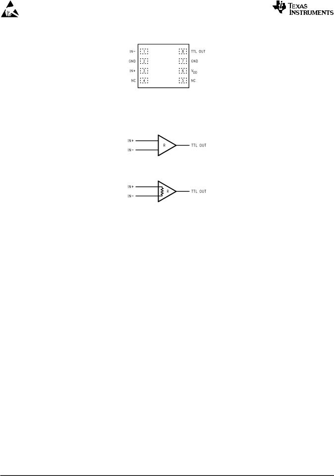
Connection Diagram
DESCRIPTION
The DS90LV012A and DS90LT012A are single CMOS differential line receivers designed for applications requiring ultra low power dissipation, low noise, and high data rates. The devices are designed to support data rates in excess of 400 Mbps (200 MHz) utilizing Low Voltage Differential Swing (LVDS) technology
The DS90LV012A and DS90LT012A accept low voltage (350 mV typical) differential input signals and translates them to 3V CMOS output levels. The receivers also support open, shorted, and terminated (100Ω) input fail-safe. The receiver output will be HIGH for all fail-safe conditions. The DS90LV012A has a pinout designed for easy PCB layout. The DS90LT012A includes an input line termination resistor for point-to-point applications.
The DS90LV012A and DS90LT012A, and companion LVDS line driver provide a new alternative to high power PECL/ECL devices for high speed interface applications.
Figure 1. Top View
See Package Number DBV (R-PDSO-G5)
Please be aware that an important notice concerning availability, standard warranty, and use in critical applications of
Texas Instruments semiconductor products and disclaimers thereto appears at the end of this data sheet.
All trademarks are the property of their respective owners.
PRODUCTION DATA information is current as of publication date. |
Copyright © 2002–2013, Texas Instruments Incorporated |
Products conform to specifications per the terms of the Texas |
|
Instruments standard warranty. Production processing does not |
|
necessarily include testing of all parameters. |
|
DS90LT012A, DS90LV012A
SNLS141D –AUGUST 2002–REVISED APRIL 2013 |
www.ti.com |
Figure 2. Top View
See Package Number NGK0008A
Functional Diagram
Figure 3. DS90LV012A
Figure 4. DS90LT012A
Truth Table
INPUTS |
OUTPUT |
|
|
[IN+] − [IN−] |
TTL OUT |
VID ≥ 0V |
H |
VID ≤ −0.1V |
L |
Full Fail-safe OPEN/SHORT or Terminated |
H |
|
|
These devices have limited built-in ESD protection. The leads should be shorted together or the device placed in conductive foam during storage or handling to prevent electrostatic damage to the MOS gates.
2 |
Submit Documentation Feedback |
Copyright © 2002–2013, Texas Instruments Incorporated |
Product Folder Links: DS90LT012A DS90LV012A

|
DS90LT012A, DS90LV012A |
www.ti.com |
SNLS141D –AUGUST 2002–REVISED APRIL 2013 |
Absolute Maximum Ratings (1) |
|
Supply Voltage (VDD) |
−0.3V to +4V |
Input Voltage (IN+, IN−) |
−0.3V to +3.9V |
Output Voltage (TTL OUT) |
−0.3V to (VDD + 0.3V) |
Output Short Circuit Current |
−100mA |
Maximum Package Power Dissipation @ +25°C |
|
|
|
NGK Package |
2.26 W |
|
|
Derate NGK Package |
18.1 mW/°C above +25°C |
|
|
Thermal resistance (θJA) |
55.3°C/W |
DBV Package |
902mW |
|
|
Derate DBV Package |
7.22 mW/°C above +25°C |
|
|
Thermal resistance (θJA) |
138.5°C/W |
Storage Temperature Range |
−65°C to +150°C |
Lead Temperature Range Soldering (4 sec.) |
+260°C |
|
|
Maximum Junction Temperature |
+150°C |
|
|
ESD Ratings (2) |
|
(1)“Absolute Maximum Ratings” are those values beyond which the safety of the device cannot be ensured. They are not meant to imply that the devices should be operated at these limits. Electrical Characteristics specifies conditions of device operation.
(2)ESD Ratings:
(a)DS90LV012A:
(a)HBM (1.5 kΩ, 100 pF) ≥ 2kV
(b)EIAJ (0Ω, 200 pF) ≥ 900V
(c)CDM ≥ 2000V
(d)IEC direct (330Ω, 150 pF) ≥ 5kV
(b)DS90LT012A:
(a)HBM (1.5 kΩ, 100 pF) ≥ 2kV
(b)EIAJ (0Ω, 200 pF) ≥ 700V
(c)CDM ≥ 2000V
(d)IEC direct (330Ω, 150 pF) ≥ 7kV
Recommended Operating Conditions
|
Min |
Typ |
Max |
Units |
|
|
|
|
|
Supply Voltage (VDD) |
+2.7 |
+3.3 |
+3.6 |
V |
Operating Free Air Temperature (TA) |
−40 |
25 |
+85 |
°C |
Electrical Characteristics
Over Supply Voltage and Operating Temperature ranges, unless otherwise specified. (1) (2)
(1)Current into device pins is defined as positive. Current out of device pins is defined as negative. All voltages are referenced to ground unless otherwise specified (such as VID).
(2)All typicals are given for: VDD = +3.3V and TA = +25°C.
Copyright © 2002–2013, Texas Instruments Incorporated |
Submit Documentation Feedback |
3 |
Product Folder Links: DS90LT012A DS90LV012A

DS90LT012A, DS90LV012A
SNLS141D –AUGUST 2002–REVISED APRIL 2013 www.ti.com
Electrical Characteristics (continued)
Over Supply Voltage and Operating Temperature ranges, unless otherwise specified. (1) (2)
Symbol |
Parameter |
Conditions |
Pin |
Min |
Typ |
Max |
Units |
|
|
|
|
|
|
|
|
|
|
VTH |
Differential Input High Threshold |
|
(3) |
IN+, IN− |
|
−30 |
0 |
mV |
VCM dependant on VDD |
|
|||||||
VTL |
Differential Input Low Threshold |
|
|
|
−100 |
−30 |
|
mV |
VCM |
Common-Mode Voltage |
VDD = 2.7V, VID = 100mV |
|
0.05 |
|
2.35 |
V |
|
|
|
VDD = 3.0V to 3.6V, VID = 100mV |
|
0.05 |
|
VDD - 0.3V |
V |
|
IIN |
Input Current (DS90LV012A) |
VIN = +2.8V |
VDD = 3.6V or 0V |
|
−10 |
±1 |
+10 |
μA |
|
|
VIN = 0V |
|
|
−10 |
±1 |
+10 |
μA |
|
|
VIN = +3.6V |
VDD = 0V |
|
−20 |
|
+20 |
μA |
IIN |
Change in Magnitude of IIN |
VIN = +2.8V |
VDD = 3.6V or 0V |
|
|
4 |
|
μA |
|
|
VIN = 0V |
|
|
|
4 |
|
μA |
|
|
VIN = +3.6V |
VDD = 0V |
|
|
4 |
|
μA |
IIND |
Differential Input Current |
VIN+ = +0.4V, VIN− = +0V |
|
3 |
3.9 |
4.4 |
mA |
|
|
(DS90LT012A) |
VIN+ = +2.4V, VIN− = +2.0V |
|
|||||
|
|
|
|
|
|
|||
RT |
Integrated Termination Resistor |
|
|
|
|
102 |
|
Ω |
|
(DS90LT012A) |
|
|
|
|
|
||
|
|
|
|
|
|
|
|
|
|
|
|
|
|
|
|
|
|
CIN |
Input Capacitance |
IN+ = IN− = GND |
|
|
3 |
|
pF |
|
VOH |
Output High Voltage |
IOH = −0.4 mA, VID = +200 mV |
TTL OUT |
2.4 |
3.1 |
|
V |
|
|
|
IOH = −0.4 mA, Inputs terminated |
|
2.4 |
3.1 |
|
V |
|
|
|
IOH = −0.4 mA, Inputs shorted |
|
2.4 |
3.1 |
|
V |
|
VOL |
Output Low Voltage |
IOL = 2 mA, VID = −200 mV |
|
|
0.3 |
0.5 |
V |
|
IOS |
Output Short Circuit Current |
VOUT = 0V (4) |
|
|
−15 |
−50 |
−100 |
mA |
VCL |
Input Clamp Voltage |
ICL = −18 mA |
|
|
−1.5 |
−0.7 |
|
V |
IDD |
No Load Supply Current |
Inputs Open |
|
VDD |
|
5.4 |
9 |
mA |
(3)VDD is always higher than IN+ and IN− voltage. IN+ and IN− are allowed to have voltage range −0.05V to +2.35V when VDD = 2.7V and |VID| / 2 to VDD − 0.3V when VDD = 3.0V to 3.6V. VID is not allowed to be greater than 100 mV when VCM = 0.05V to 2.35V when VDD = 2.7V or when VCM = |VID| / 2 to VDD − 0.3V when VDD = 3.0V to 3.6V.
(4)Output short circuit current (IOS) is specified as magnitude only, minus sign indicates direction only. Only one output should be shorted at a time, do not exceed maximum junction temperature specification.
4 |
Submit Documentation Feedback |
Copyright © 2002–2013, Texas Instruments Incorporated |
Product Folder Links: DS90LT012A DS90LV012A

DS90LT012A, DS90LV012A
www.ti.com SNLS141D –AUGUST 2002–REVISED APRIL 2013
Switching Characteristics
Over Supply Voltage and Operating Temperature ranges, unless otherwise specified. (1) (2)
Symbol |
Parameter |
Conditions |
Min |
Typ |
Max |
Units |
|
|
|
|
|
|
|
tPHLD |
Differential Propagation Delay High to Low |
CL = 15 pF |
1.0 |
1.8 |
3.5 |
ns |
tPLHD |
Differential Propagation Delay Low to High |
VID = 200 mV |
1.0 |
1.7 |
3.5 |
ns |
tSKD1 |
Differential Pulse Skew |tPHLD − tPLHD| (3) |
(Figure 5 and Figure 6) |
0 |
100 |
400 |
ps |
t |
Differential Part to Part Skew (4) |
|
0 |
0.3 |
1.0 |
ns |
SKD3 |
|
|
|
|
|
|
t |
Differential Part to Part Skew (5) |
|
0 |
0.4 |
1.5 |
ns |
SKD4 |
|
|
|
|
|
|
tTLH |
Rise Time |
|
|
350 |
800 |
ps |
tTHL |
Fall Time |
|
|
175 |
800 |
ps |
f |
Maximum Operating Frequency (6) |
|
200 |
250 |
|
MHz |
MAX |
|
|
|
|
|
|
(1)CL includes probe and jig capacitance.
(2)Generator waveform for all tests unless otherwise specified: f = 1 MHz, ZO = 50Ω, tr and tf (0% to 100%) ≤ 3 ns for IN±.
(3)tSKD1 is the magnitude difference in differential propagation delay time between the positive-going-edge and the negative-going-edge of the same channel.
(4)tSKD3, part to part skew, is the differential channel-to-channel skew of any event between devices. This specification applies to devices at the same VDD and within 5°C of each other within the operating temperature range.
(5)tSKD4, part to part skew, is the differential channel-to-channel skew of any event between devices. This specification applies to devices over the recommended operating temperature and voltage ranges, and across process distribution. tSKD4 is defined as |Max − Min| differential propagation delay.
(6)fMAX generator input conditions: tr = tf < 1 ns (0% to 100%), 50% duty cycle, differential (1.05V to 1.35 peak to peak). Output criteria: 60%/40% duty cycle, VOL (max 0.4V), VOH (min 2.4V), load = 15 pF (stray plus probes). The parameter is ensured by design. The limit is based on the statistical analysis of the device over the PVT range by the transition times (tTLH and tTHL).
Copyright © 2002–2013, Texas Instruments Incorporated |
Submit Documentation Feedback |
5 |
Product Folder Links: DS90LT012A DS90LV012A

DS90LT012A, DS90LV012A
SNLS141D –AUGUST 2002–REVISED APRIL 2013 |
www.ti.com |
PARAMETER MEASUREMENT INFORMATION
Figure 5. Receiver Propagation Delay and Transition Time Test Circuit
Figure 6. Receiver Propagation Delay and Transition Time Waveforms
TYPICAL APPLICATIONS
Balanced System
Figure 7. Point-to-Point Application (DS90LV012A)
Balanced System
Figure 8. Point-to-Point Application (DS90LT012A)
6 |
Submit Documentation Feedback |
Copyright © 2002–2013, Texas Instruments Incorporated |
Product Folder Links: DS90LT012A DS90LV012A
Loading...