


 Loading...
DAC8552
 DAC8552
SLAS430A – JULY 2006 – REVISED OCTOBER 2006
16-BIT, DUAL CHANNEL, ULTRA-LOW GLITCH, VOLTAGE OUTPUT
DIGITAL-TO-ANALOG CONVERTER
FEATURES
∙Relative Accuracy: 4LSB
∙Glitch Energy: 0.15nV-s
∙MicroPower Operation: 155μA per Channel at 2.7V
∙Power-On Reset to Zero-Scale
∙Power Supply: 2.7V to 5.5V
∙16-Bit Monotonic Over Temperature
∙Settling Time: 10μs to ±0.003% FSR
∙Ultra-Low AC Crosstalk: –100dB Typ
∙Low-Power Serial Interface with Schmitt-Triggered Inputs
∙On-Chip Output Buffer Amplifier with Rail-to-Rail Operation
∙Double-Buffered Input Architecture
∙Simultaneous or Sequential Output Update and Power-down
∙Available in a Tiny MSOP-8 Package
APPLICATIONS
∙Portable Instrumentation
∙Closed-Loop Servo Control
∙Process Control
∙Data Acquisition Systems
∙Programmable Attenuation
∙PC Peripherals
DESCRIPTION
The DAC8552 is a 16-bit, dual channel, voltage output digital-to-analog converter (DAC) offering low power operation and a flexible serial host interface. Each on-chip precision output amplifier allows rail-to-rail output swing to be achieved over the supply range of 2.7V to 5.5V. The device supports a standard 3-wire serial interface capable of operating with input data clock frequencies up to 30MHz for VDD = 5V.
The DAC8552 requires an external reference voltage to set the output range of each DAC channel. Also incorporated into the device is a power-on reset circuit which ensures that the DAC outputs power up at zero-scale and remain there until a valid write takes place. The DAC8552 provides a flexible power-down feature, accessed over the serial interface, that reduces the current consumption of the device to 700nA at 5V.
The low-power consumption of this device in normal operation makes it ideally suited for portable, battery-operated equipment and other low-power applications. The power consumption is 0.5mW per channel at 2.7V, reducing to 1μW in power-down mode.
The DAC8552 is available in a MSOP-8 package with a specified operating temperature range of –40°C to +105°C.
|
VDD |
|
|
VREF |
|
|
|
|
|
Data |
DAC |
DAC A |
VOUTA |
|
|
|
Buffer A |
Register A |
||
|
|
|
Data |
DAC |
DAC B |
VOUTB |
|
|
|
Buffer B |
Register B |
||
|
|
|
|
|
||
|
16 |
|
|
|
|
|
SYNC |
24-Bit, |
|
Channel |
Load |
|
|
Serial-to- |
|
|
Power-Down |
|||
|
|
Select |
Control |
|
||
SCLK |
Parallel |
|
|
Control Logic |
||
|
|
|
|
|||
Shift |
8 |
Control Logic |
|
2 |
||
|
|
|||||
DIN |
Register |
|
|
|
|
Resistor |
|
|
|
|
Network |
||
|
GND |
|
|
|
|
|
Please be aware that an important notice concerning availability, standard warranty, and use in critical applications of Texas Instruments semiconductor products and disclaimers thereto appears at the end of this data sheet.
SPI, QSP are trademarks of Motorola, Inc. Microwire is a trademark of National Semiconductor.
All other trademarks are the property of their respective owners.
PRODUCTION DATA information is current as of publication date. |
Copyright © 2006, Texas Instruments Incorporated |
Products conform to specifications per the terms of the Texas |
|
Instruments standard warranty. Production processing does not |
|
necessarily include testing of all parameters. |
|
DAC8552
www.ti.com
SLAS430A – JULY 2006 – REVISED OCTOBER 2006
This integrated circuit can be damaged by ESD. Texas Instruments recommends that all integrated circuits be handled with appropriate precautions. Failure to observe proper handling and installation procedures can cause damage.
ESD damage can range from subtle performance degradation to complete device failure. Precision integrated circuits may be more susceptible to damage because very small parametric changes could cause the device not to meet its published specifications.
PACKAGING/ORDERING INFORMATION(1)
|
MAXIMUM |
MAXIMUM |
|
|
|
|
|
|
|
|
RELATIVE |
DIFFERENTIAL |
|
|
SPECIFICATION |
|
|
TRANSPORT |
|
|
ACCURACY |
NONLINEARITY |
PACKAGE |
PACKAGE |
TEMPERATURE |
PACKAGE |
ORDERING |
MEDIA, |
|
PRODUCT |
(LSB) |
(LSB) |
LEAD |
DESIGNATOR |
RANGE |
MARKING |
NUMBER |
QUANTITY |
|
DAC8552 |
±12 |
±1 |
MSOP-8 |
DGK |
–40°C to +105°C |
D82 |
DAC8552IDGKT |
Tape and Reel, 250 |
|
DAC8552IDGKR |
Tape and Reel, 2500 |
||||||||
|
|
|
|
|
|
|
(1)For the most current package and ordering information, see the Package Option Addendum at the of this document, or see the TI website at www.ti.com.
ABSOLUTE MAXIMUM RATINGS
over operating free-air temperature range (unless otherwise noted).(1)
|
|
UNIT |
|
VDD to GND |
|
–0.3V to 6V |
|
Digital input voltage to GND |
–0.3V to VDD + 0.3V |
||
VOUTA or VOUTB to GND |
|
–0.3V to VDD + 0.3V |
|
Operating temperature range |
–40°C to +105°C |
||
Storage temperature range |
–65°C to +150°C |
||
Junction temperature (TJ max) |
+150°C |
||
Power dissipation |
|
(TJ max – TA)/θJA |
|
Thermal impedance |
θJA |
206°C/W |
|
θJC |
44°C/W |
||
|
|||
(1)Stresses above those listed under Absolute Maximum Ratings may cause permanent damage to the device. Exposure to absolute maximum conditions for extended periods may affect device reliability.
ELECTRICAL CHARACTERISTICS
VDD = 2.7V to 5.5V, all specifications –40°C to +105°C (unless otherwise noted).
PARAMETER |
TEST CONDITIONS |
MIN |
TYP |
MAX |
UNIT |
STATIC PERFORMANCE(1) |
|
|
|
|
|
Resolution |
|
16 |
|
|
Bits |
Relative accuracy |
Measured by line passing through codes 513 and |
|
±4 |
±12 |
LSB |
|
64741 |
|
|
|
|
Differential nonlinearity |
16-bit monotonic |
|
±0.35 |
±1 |
LSB |
Zero code error |
Measured by line passing through codes 485 and |
|
±2.5 |
±12 |
mV |
|
64741 |
|
|
|
|
Zero code error drift |
|
|
±5 |
|
μV/°C |
Full-scale error |
Measured by line passing through codes 485 and |
|
±0.1 |
±0.5 |
% of FSR |
|
64741 |
|
|
|
|
Gain error |
Measured by line passing through codes 485 and |
|
±0.08 |
±0.2 |
% of FSR |
|
64741 |
|
|
|
|
Gain temperature coefficient |
|
|
±1 |
|
ppm of FSR/°C |
PSRR |
Output unloaded |
|
0.75 |
|
mV/V |
(1)Linearity calculated using a reduced code range of 513 to 64741. Output unloaded.
2 |
Submit Documentation Feedback |
DAC8552
www.ti.com
SLAS430A – JULY 2006 – REVISED OCTOBER 2006
ELECTRICAL CHARACTERISTICS (continued)
VDD = 2.7V to 5.5V, all specifications –40°C to +105°C (unless otherwise noted).
PARAMETER
 OUTPUT CHARACTERISTICS(2)
Output voltage range
Output voltage settling time
 Slew rate
 Capacitive load stability
Code change glitch impulse  Digital feedthrough
DC crosstalk
 AC crosstalk
DC output impedance
 Short circuit current
 Power-up time
AC PERFORMANCE
 SNR
SNR
THD
 SFDR
SFDR
SINAD
 REFERENCE INPUT
 Reference current
Reference input range
 Reference input impedance
LOGIC INPUTS(2)
 Input current
 VINL, Input LOW voltage
 VINH, Input HIGH voltage
Pin capacitance
 POWER REQUIREMENTS
VDD
IDD (normal mode)
VDD = 3.6V to 5.5V
VDD = 2.7V to 3.6V
 IDD (all power-down modes) VDD = 3.6V to 5.5V
VDD = 2.7V to 3.6V
POWER EFFICIENCY
IOUT/IDD
 TEMPERATURE RANGE
Specified performance
TEST CONDITIONS |
MIN |
TYP |
MAX |
UNIT |
|
0 |
|
VREF |
V |
To ±0.003% FSR 0200h to FD00h, RL = 2kΩ; |
|
8 |
10 |
|
0pF < CL < 200pF |
|
μ |
||
|
|
|
||
|
|
|
|
s |
RL = 2kΩ; CL = 500pF |
|
12 |
|
|
|
|
1.8 |
|
V/μs |
RL = ∞ |
|
470 |
|
pF |
RL = 2kΩ |
|
1000 |
|
|
|
|
|
||
1LSB change around major carry |
|
0.15 |
|
nV-s |
50kΩ series resistance on digital lines |
|
0.15 |
|
nV-s |
Full-scale swing on adjacent channel. |
|
0.25 |
|
LSB |
VDD = 5V, VREF = 4.096V |
|
|
||
|
|
|
|
|
1kHz sine wave |
|
–100 |
|
dB |
At mid-point input |
|
1 |
|
Ω |
VDD = 5V |
|
50 |
|
mA |
VDD = 3V |
|
20 |
|
|
|
|
|
||
Coming out of power-down mode, VDD = 5V |
|
2.5 |
|
μs |
Coming out of power-down mode, VDD = 3V |
|
5 |
|
μs |
|
|
95 |
|
|
BW = 20kHz, VDD = 5V, fOUT = 1kHz, |
|
–85 |
|
dB |
|
|
|
||
1st 19 harmonics removed for SNR calculation |
|
87 |
|
|
|
|
|
||
|
|
|
|
|
|
|
84 |
|
|
VREF = VDD = 5.5V |
|
90 |
120 |
μA |
VREF = VDD = 3.6V |
|
60 |
100 |
|
|
|
|||
|
0 |
|
VDD |
V |
|
|
62 |
|
kΩ |
|
|
|
±1 |
μA |
VDD = 5V |
|
|
0.8 |
V |
VDD = 3V |
|
|
0.6 |
|
|
|
|
||
VDD = 5V |
2.4 |
|
|
V |
VDD = 3V |
2.1 |
|
|
|
|
|
|
||
|
|
|
3 |
pF |
|
2.7 |
|
5.5 |
V |
Input code = 32768, no load, does not include |
|
|
|
|
reference current |
|
|
|
|
VIH = VDD and VIL = GND |
|
340 |
500 |
μA |
|
310 |
480 |
||
|
|
|
||
VIH = VDD and VIL = GND |
|
0.7 |
2 |
μA |
|
0.4 |
2 |
||
|
|
|
||
ILOAD = 2mA, VDD = 5V |
|
89 |
|
% |
|
–40 |
|
+105 |
°C |
(2)Specified by design and characterization; not production tested.
Submit Documentation Feedback |
3 |
DAC8552
www.ti.com
SLAS430A – JULY 2006 – REVISED OCTOBER 2006
PIN CONFIGURATION
DGK PACKAGE
MSOP-8
(Top View)
VDD |
|
|
|
|
GND |
1 |
|
8 |
|
||
VREF |
|
|
|
|
DIN |
2 |
|
7 |
|
||
VOUTB |
|
DAC8552 |
|
|
SCLK |
|
|
|
|||
3 |
|
6 |
|
||
|
|
|
|
|
|
VOUTA |
4 |
|
5 |
|
SYNC |
|
|
|
|
|
|
|
|
PIN DESCRIPTIONS |
PIN |
NAME |
FUNCTION |
1 |
VDD |
Power supply input, 2.7V to 5.5V |
2 |
VREF |
Reference voltage input |
3 |
VOUTB |
Analog output voltage from DAC B |
4 |
VOUTA |
Analog output voltage from DAC A |
|
|
Level triggered SYNC input (active LOW). This is the frame synchronization signal for the input data. When SYNC goes |
|
|
LOW, it enables the input shift register and data is transferred on the falling edges of SCLK. The action specified by the |
5 |
SYNC |
8-bit control byte and 16-bit data word is executed following the 24th falling SCLK clock edge (unless SYNC is taken |
|
|
HIGH before this edge, in which case the rising edge of SYNC acts as an interrupt and the write sequence is ignored |
|
|
by the DAC8552). Schmitt-Trigger logic input. |
6 |
SCLK |
Serial Clock Input. Data can be transferred at rates up to 30MHz at 5V. Schmitt-Trigger logic input. |
7 |
DIN |
Serial Data Input. Data is clocked into the 24-bit input shift register on the falling edge of the serial clock input. |
Schmitt-Trigger logic input. |
||
8 |
GND |
Ground reference point for all circuitry on the part. |
4 |
Submit Documentation Feedback |
DAC8552
www.ti.com
SLAS430A – JULY 2006 – REVISED OCTOBER 2006
SERIAL WRITE OPERATION
|
t1 |
|
t9 |
SCLK |
1 |
24 |
|
|
t8 |
t2 |
|
|
t3 |
|
|
|
t7 |
|
|
|
t4 |
|
|
SYNC |
|
|
|
|
t6 |
|
|
|
t5 |
|
|
DIN |
DB23 |
DB0 |
DB23 |
TIMING CHARACTERISTICS(1) (2)
VDD = 2.7V to 5.5V, all specifications –40°C to +105°C (unless otherwise noted).
|
PARAMETER |
TEST CONDITIONS |
MIN TYP MAX |
UNIT |
|
t (3) |
SCLK cycle time |
VDD = 2.7V to 3.6V |
50 |
ns |
|
|
|
||||
1 |
|
VDD = 3.6V to 5.5V |
33 |
|
|
|
|
|
|||
t2 |
SCLK HIGH time |
VDD = 2.7V to 3.6V |
13 |
ns |
|
VDD = 3.6V to 5.5V |
13 |
||||
|
|
|
|||
t3 |
SCLK LOW time |
VDD = 2.7V to 3.6V |
22.5 |
ns |
|
VDD = 3.6V to 5.5V |
13 |
||||
|
|
|
|||
t4 |
SYNC to SCLK rising edge setup time |
VDD = 2.7V to 3.6V |
0 |
ns |
|
VDD = 3.6V to 5.5V |
0 |
||||
|
|
|
|||
t5 |
Data setup time |
VDD = 2.7V to 3.6V |
5 |
ns |
|
VDD = 3.6V to 5.5V |
5 |
||||
|
|
|
|||
t6 |
Data hold time |
VDD = 2.7V to 3.6V |
4.5 |
ns |
|
VDD = 3.6V to 5.5V |
4.5 |
||||
|
|
|
|||
t7 |
24th SCLK falling edge to SYNC rising edge |
VDD = 2.7V to 3.6V |
0 |
ns |
|
VDD = 3.6V to 5.5V |
0 |
||||
|
|
|
|||
t8 |
Minimum SYNC HIGH time |
VDD = 2.7V to 3.6V |
50 |
ns |
|
VDD = 3.6V to 5.5V |
33 |
||||
|
|
|
|||
t9 |
24th SCLK falling edge to SYNC falling edge |
VDD = 2.7V to 5.5V |
100 |
ns |
(1)All input signals are specified with tR = tF = 5ns (10% to 90% of VDD) and timed from a voltage level of (VIL + VIH)/2.
(2)See Serial Write Operation Timing Diagram.
(3)Maximum SCLK frequency is 30MHz at VDD = 3.6V to 5.5V and 20MHz at VDD = 2.7V to 3.6V.
Submit Documentation Feedback |
5 |
DAC8552
www.ti.com
SLAS430A – JULY 2006 – REVISED OCTOBER 2006
TYPICAL CHARACTERISTICS: VDD = 5V
At TA = +25°C, unless otherwise noted.
|
|
|
|
LINEARITY ERROR AND |
|||||
|
|
DIFFERENTIAL LINEARITY ERROR vs CODE |
|||||||
|
8 |
|
|
|
|
|
|
|
|
|
VDD = 5V, VREF = 4.9V, T |
A = +25° |
C |
|
|
|
|||
|
6 |
|
|
|
|||||
LE(LSB) |
4 |
Channel A Output |
|
|
|
|
|
||
2 |
|
|
|
|
|
|
|
|
|
|
|
|
|
|
|
|
|
|
|
|
0 |
|
|
|
|
|
|
|
|
|
|
|
|
|
|
|
|
|
|
|
−2 |
|
|
|
|
|
|
|
|
|
|
|
|
|
|
|
|
|
|
|
−4 |
|
|
|
|
|
|
|
|
|
|
|
|
|
|
|
|
|
|
|
−6 |
|
|
|
|
|
|
|
|
|
|
|
|
|
|
|
|
|
|
|
−8 |
|
|
|
|
|
|
|
|
DLE(LSB) |
1.0 |
|
|
|
|
|
|
|
|
|
|
|
|
|
|
|
|
||
0.5 |
|
|
|
|
|
|
|
|
|
|
|
|
|
|
|
|
|
||
−0.5 |
|
|
|
|
|
|
|
|
|
|
0 |
|
|
|
|
|
|
|
|
|
−1.0 |
|
|
|
|
|
|
|
|
|
|
|
|
|
|
|
|
|
|
08192 16384 24576 32768 40960 49152 57344 65536
Digital Input Code
Figure 1.
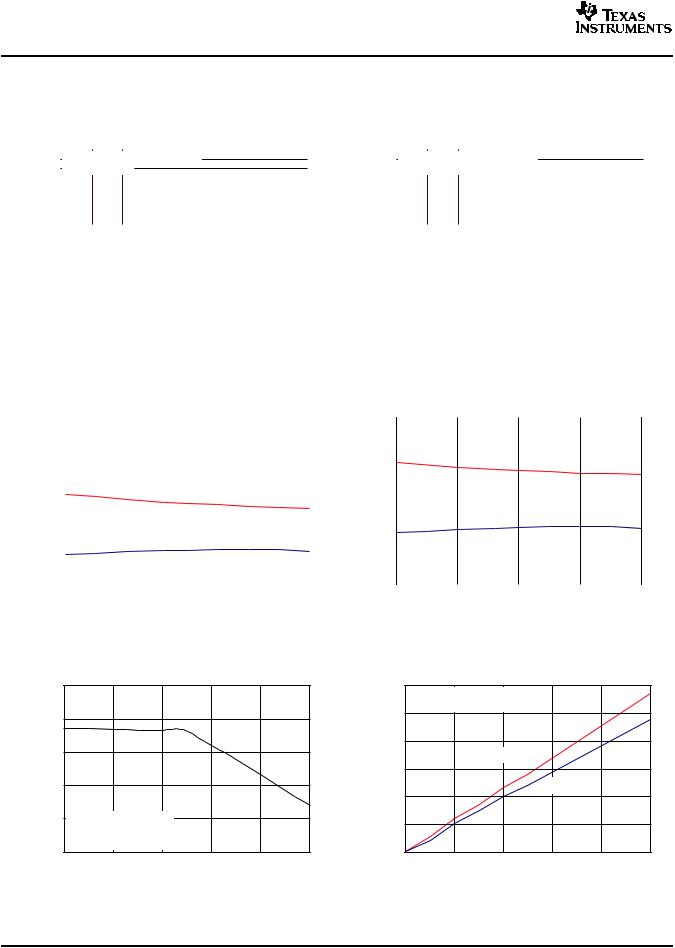
ZERO-SCALE ERROR vs TEMPERATURE
|
7.5 |
|
|
|
|
|
|
|
|
|
|
|
VDD = 5V |
|
|
|
|
|
|
|
|
|
5.0 |
VREF = 4.99V |
|
|
|
|
|
|
|
|
(mV) |
|
|
|
|
|
|
|
|
|
|
2.5 |
|
|
|
|
|
|
|
|
|
|
|
|
|
|
|
|
|
|
|
||
ScaleError |
|
|
|
|
CH B |
|
|
|
|
|
|
|
|
|
|
|
|
|
|
|
|
- |
0 |
|
|
|
|
|
|
|
|
|
|
|
|
|
|
|
|
|
|
||
−2.5 |
|
|
|
|
|
|
|
|
|
|
Zero |
|
|
|
CH A |
|
|
|
|
|
|
|
|
|
|
|
|
|
|
|
||
|
−5.0 |
|
|
|
|
|
|
|
|
|
|
|
|
|
|
|
|
|
|
|
|
|
−7.5 |
|
|
|
|
|
|
|
|
|
|
|
|
|
|
|
|
|
|
|
|
|
−40 |
0 |
40 |
80 |
120 |
|||||
|
|
|
|
|
Temperature (°C) |
|
|
|
|
|
Figure 3.
|
|
|
|
LINEARITY ERROR AND |
|||||
|
|
DIFFERENTIAL LINEARITY ERROR vs CODE |
|||||||
|
8 |
|
|
|
|
|
|
|
|
|
VDD = 5V, VREF = 4.9V, T |
A = +25° |
C |
|
|
|
|||
|
6 |
|
|
|
|||||
|
4 |
|
|
|
|
|
|
|
|
LE(LSB) |
Channel B Output |
|
|
|
|
|
|||
2 |
|
|
|
|
|
|
|
|
|
|
|
|
|
|
|
|
|
|
|
|
0 |
|
|
|
|
|
|
|
|
|
|
|
|
|
|
|
|
|
|
|
−2 |
|
|
|
|
|
|
|
|
|
|
|
|
|
|
|
|
|
|
|
−4 |
|
|
|
|
|
|
|
|
|
|
|
|
|
|
|
|
|
|
|
−6 |
|
|
|
|
|
|
|
|
|
|
|
|
|
|
|
|
|
|
|
−8 |
|
|
|
|
|
|
|
|
DLE(LSB) |
1.0 |
|
|
|
|
|
|
|
|
|
|
|
|
|
|
|
|
||
0.5 |
|
|
|
|
|
|
|
|
|
|
|
|
|
|
|
|
|
||
−0.5 |
|
|
|
|
|
|
|
|
|
|
0 |
|
|
|
|
|
|
|
|
|
−1.0 |
|
|
|
|
|
|
|
|
|
|
|
|
|
|
|
|
|
|
08192 16384 24576 32768 40960 49152 57344 65536
Digital Input Code
Figure 2.
|
|
FULL-SCALE ERROR |
|
|
vs TEMPERATURE |
|
5 |
|
|
VDD = 5V |
|
|
|
|
|
|
VREF = 4.99V |
(mV)ScaleError |
|
CH B |
0 |
CH A |
|
|
|
|
- |
−5 |
|
Full |
|
|
−10 |
|
|
|
|
|
|
|
|
|
|
|
|
|
−40 |
0 |
40 |
80 |
120 |
||
|
|
|
Temperature (°C) |
|
|
|
Figure 4.
SOURCE CURRENT CAPABILITY
AT POSITIVE RAIL
|
6.0 |
|
|
5.6 |
|
(V) |
5.2 |
|
|
|
|
OUT |
|
|
V |
4.8 |
|
|
|
|
|
4.4 |
VDD = 5.5V |
|
|
VREF = VDD − 10mV |
DAC Loaded with FFFFh
4.0
0 |
2 |
4 |
6 |
8 |
10 |
ISOURCE (mA)
Figure 5.
SINK CURRENT CAPABILTY
AT NEGATIVE RAIL
|
0.150 |
VREF = VDD − 10mV |
|
|
|
|
|
|
|
|
|
|
|
|
0.125 |
DAC Loaded with 0000h |
|
|
|
|
|
|
|
|
|
|
|
|
0.100 |
|
|
|
|
|
(V) |
|
|
VDD = 2.7V |
|
|
|
OUT |
0.075 |
|
|
|
|
|
|
|
|
|
|
|
|
V |
|
|
|
VDD |
= 5.5V |
|
|
0.050 |
|
|
|
||
|
|
|
|
|
|
|
|
0.025 |
|
|
|
|
|
|
0 |
|
|
|
|
|
|
0 |
2 |
4 |
6 |
8 |
10 |
ISINK (mA)
Figure 6.
6 |
Submit Documentation Feedback |

DAC8552
www.ti.com
SLAS430A – JULY 2006 – REVISED OCTOBER 2006
TYPICAL CHARACTERISTICS: VDD = 5V (continued)
At TA = +25°C, unless otherwise noted.
SUPPLY CURRENT |
SUPPLY CURRENT |
vs DIGITAL INPUT CODE |
vs SUPPLY VOLTAGE |
600 

 Reference Current Included
|
500 |
|
|
|
|
|
|
|
|
|
VDD = VREF = 5.5V |
|
|
|
|
||
|
400 |
|
|
|
|
|
|
|
A) |
|
|
|
|
VDD = VREF = 3.6V |
|||
( |
300 |
|
|
|
|
|
|
|
DD |
|
|
|
|
|
|
|
|
|
|
|
|
|
|
|
|
|
I |
|
|
|
|
|
|
|
|
|
200 |
|
|
|
|
|
|
|
|
100 |
|
|
|
|
|
|
|
|
0 |
|
|
|
|
|
|
|
|
0 |
8192 |
16384 |
24576 32768 |
40960 |
49152 |
57344 |
65536 |
|
|
|
|
Digital Input Code |
|
|
|
|
|
600 |
|
|
|
|
|
|
|
|
550 |
VREF = VDD, All DACs Powered |
|
|
|
|||
|
Reference Current Included, No Load |
|
|
|||||
|
500 |
|
|
|
|
|
|
|
( A) |
450 |
|
|
|
|
|
|
|
400 |
|
|
|
|
|
|
|
|
DD |
|
|
|
|
|
|
|
|
|
|
|
|
|
|
|
|
|
I |
|
|
|
|
|
|
|
|
|
350 |
|
|
|
|
|
|
|
|
300 |
|
|
|
|
|
|
|
|
250 |
|
|
|
|
|
|
|
|
200 |
|
|
|
|
|
|
|
|
|
2.7 |
3.1 |
3.5 |
4.3 |
4.7 |
5.1 |
5.5 |
VDD (V)
Figure 7. |
Figure 8. |
SUPPLY CURRENT vs TEMPERATURE
|
600 |
|
|
|
|
|
Reference Current Included |
|
|
||
|
500 |
|
|
|
|
|
|
VDD = VREF = 5.5V |
|
|
|
|
400 |
|
|
|
|
(µV) |
|
|
|
VDD = VREF = 3.6V |
|
300 |
|
|
|
|
|
DD |
|
|
|
|
|
|
|
|
|
|
|
I |
|
|
|
|
|
|
200 |
|
|
|
|
|
100 |
|
|
|
|
|
0 |
|
|
|
|
|
−40 |
0 |
40 |
80 |
120 |
|
|
|
Temperature (°C) |
|
|
Figure 9.
POWER SPECTRAL DENSITY
|
−10 |
|
|
VDD = 5V |
|
|
|
|
|
VREF = 4.096V |
|
|
−30 |
|
|
fOUT = 1kHz |
|
|
|
|
|
f |
= 1MSPS |
|
|
|
|
CLK |
|
Gain(dB) |
−50 |
|
|
|
|
−70 |
|
|
|
|
|
|
|
|
|
|
|
|
−90 |
|
|
|
|
|
−110 |
|
|
|
|
|
−130 |
|
|
|
|
|
0 |
5 |
10 |
15 |
20 |
Frequency (kHz)
Figure 11.
SUPPLY CURRENT
vs LOGIC INPUT VOLTAGE
|
2400 |
TA = 25°C, SYNC Input (all other inputs = GND) |
|
|
|||
|
|
|
|
||||
|
2000 |
CH A Powered Up; All Other Channels in Power-Down |
|
||||
|
|
|
|
|
|
|
|
|
1600 |
|
|
|
|
|
|
A) |
|
VDD = VREF = 5.5V |
|
|
|
|
|
( |
1200 |
|
|
|
|
|
|
DD |
|
|
|
|
|
|
|
|
|
|
|
|
|
|
|
I |
|
|
|
|
|
|
|
|
800 |
|
|
|
|
|
|
|
400 |
|
|
|
|
|
|
|
0 |
|
|
|
|
|
|
|
0 |
1 |
2 |
3 |
4 |
5 |
5.5 |
VLOGIC (V)
Figure 10.
TOTAL HARMONIC DISTORTION vs OUTPUT FREQUENCY
−40 VDD = 5V
−50 VREF = 4.9V -1dB FSR Digital Input
fS = 1MSPS
|
−60 |
Measurement Bandwidth = 20kHz |
|
|
||
(dB) |
−70 |
|
|
|
|
|
THD |
|
|
|
|
|
|
|
THD |
|
|
|
|
|
|
|
|
|
|
|
|
|
−80 |
|
|
|
|
|
|
−90 |
|
|
|
|
|
|
|
2nd Harmonic |
|
3rd Harmonic |
|
|
|
−100 |
|
|
|
|
|
|
0 |
1 |
2 |
3 |
4 |
5 |
fOUT (kHz)
Figure 12.
Submit Documentation Feedback |
7 |
Loading...