


Texas Instruments DV2003L1, DV2003S2, DV2003S1, BQ2003STR, BQ2003S-NTR Datasheet
...Features
Fast charge and conditioning of nickel cadmium or nickel-metal hydride batteries
Hysteretic PWM switch-mode current regulation or gated control of an external regulator
Easily integrated into systems or used as a stand-alone charger
Pre-charge qualification of temperature and voltage
Direct LED outputs display battery and charge status
Fast-charge termination by
∆ temperature/∆ time, -∆V, maximum voltage, maximum temperature, and maximum time
Optional top-off charge
bq2003
General Description
The bq2003 Fast Charge IC provides comprehensive fast charge control functions together with high-speed switching power control circuitry on a monolithic CMOS device.
Integration of closed-loop current control circuitry allows the bq2003 to be the basis of a cost-effective solution for stand-alone and systemintegrated chargers for batteries of one or more cells.
Switch-activated discharge-before- charge allows bq2003-based chargers to support battery conditioning and capacity determination.
High-efficiency power conversion is accomplished using the bq2003 as a hysteretic PWM controller for switch-mode regulation of the charging current. The bq2003 may alternatively be used to gate an externally regulated charging current.
Fast-Charge IC
Fast charge may begin on application of the charging supply, replacement of the battery, or switch depression. For safety, fast charge is inhibited unless/until the battery temperature and voltage are within configured limits.
Temperature, voltage, and time are monitored throughout fast charge. Fast charge is terminated by any of the following:
Rate of temperature rise (∆T/∆t)
Negative delta voltage (-∆V)
Maximum voltage
Maximum temperature
Maximum time
After fast charge, an optional top-off phase is available. Constant-cur- rent maintenence charge is provided by an external trickle resistor.
Pin Connections |
|
Pin Names |
|
|
|||||
|
|
|
|
|
|
CCMD |
Charge command/select |
SNS |
Sense resistor input |
|
|
|
|
|
|
||||
|
|
|
|
|
|
DCMD |
Discharge command |
TCO |
Temperature cutoff |
|
|
|
|
|
|
||||
CCMD |
|
1 |
16 |
|
VCC |
DVEN |
-∆V enable/disable |
MCV |
Maximum voltage |
|
|
|
|
|
|
||||
DCMD |
|
2 |
15 |
|
DIS |
TM1 |
Timer mode select 1 |
TEMP |
Temperature status |
DVEN |
|
3 |
14 |
|
MOD |
||||
|
|
TM2 |
Timer mode select 2 |
|
output |
||||
TM1 |
|
4 |
13 |
|
CHG |
CHG |
Charging status output |
||
|
|
|
|
||||||
|
|
|
|
|
|
TS |
Temperature sense |
||
TM2 |
|
5 |
12 |
|
TEMP |
MOD |
Charge current control |
||
TS |
|
6 |
11 |
|
MCV |
BAT |
Battery voltage |
||
|
|
DIS |
Discharge control |
||||||
BAT |
|
7 |
10 |
|
TCO |
VSS |
System ground |
||
|
|
|
|
||||||
|
|
|
|
|
|
VCC |
5.0V ±10% power |
||
VSS |
|
8 |
9 |
|
SNS |
|
|
||
|
|
|
|
|
|
|
|
|
|
|
16-Pin DIP or SOIC |
|
|
|
|
|
|||
|
|
|
PN200301.eps |
|
|
|
|
|
|
|
|
|
|
|
|
|
|
|
|
SLUS095A - OCTOBER 1999 I
1

bq2003
Pin Descriptions
CCMD, |
Charge initiation and discharge-before- |
DCMD |
charge control inputs |
|
These two inputs control the conditions that |
|
begin a new charge cycle and enable |
|
discharge-before-charge. See Table 1. |
DVEN |
-∆V enable input |
|
This input enales/disables -∆V charge termina- |
|
tion. If DVEN is high, the -∆V test is enabled. |
|
If DVEN is low, -∆V test is disabled. The state |
|
of DVEN may be changed at any time. |
TM1– |
Timer mode inputs |
TM2 |
TM1 and TM2 are three-state inputs that con- |
|
|
|
figure the fast charge safety timer, -∆V hold- |
|
off time, and that enhance/disable top-off. |
|
See Table 2. |
TS |
Temperature sense input |
|
Input, referenced to SNS, for an external |
|
thermistor monitoring battery temperature. |
BAT |
Single-cell voltage input |
|
The battery voltage sense input, referenced |
|
to SNS. This is created by a high-impedance |
|
resistor divider network connected between |
|
the positive and the negative terminals of |
|
the battery. |
Vss |
Ground |
SNS |
Charging current sense input |
|
SNS controls the switching of MOD based on |
|
the voltage across an external sense resistor |
|
in the current path of the battery. SNS is the |
|
reference potential for the TS and BAT pins. |
|
If SNS is connected to VSS, MOD switches |
|
high at the beginning of charge and low at |
|
the end of charge. |
TCO |
Temperature cutoff threshold input |
|
Input to set maximum allowable battery |
|
temperature. If the potential between TS |
|
and SNS is less than the voltage at the TCO |
|
input, then fast charge or top-off charge is |
|
terminated. |
MCV |
Maximum-Cell-Voltage threshold input |
|
Input to set maximum single-cell equivalent |
|
voltage. If the voltage between BAT and SNS |
|
is greater than or equal to the voltage at the |
|
MCV input, then fast charge or top-off charge |
|
is inhibited. |
|
Note: For valid device operation, the |
|
voltage level on MCV must not exceed |
|
0.6 VCC. |
TEMP |
Temperature status output |
|
Push-pull output indicating temperature |
|
status. TEMP is low if the voltage at the TS |
|
pin is not within the allowed range to start |
|
fast charge. |
CHG |
Charging status output |
|
Push-pull output indicating charging status. |
|
See Figure 1. |
MOD |
Current-switching control output |
|
MOD is a push/pull output that is used to |
|
control the charging current to the battery. |
|
MOD switches high to enable charging cur- |
|
rent flow and low to inhibit charging current |
|
flow. |
DIS |
Discharge FET control output |
|
Push-pull output used to control an external |
|
transistor to discharge the battery before |
|
charging. |
VCC |
VCC supply input |
|
5.0 V, ±10% power input. |
2
bq2003
Functional Description
Figure 3 shows a state diagram and Figure 4 shows a block diagram of the bq2003.
Battery Voltage and Temperature
Measurements
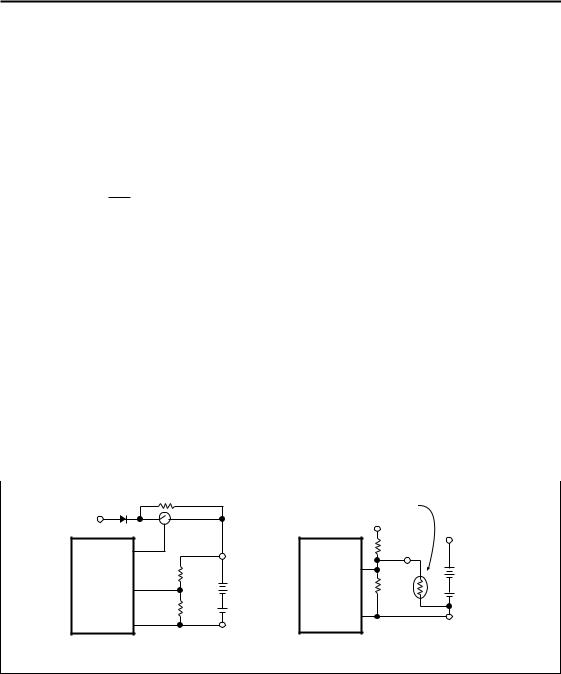
Battery voltage and temperature are monitored for maximum allowable values. The voltage presented on the battery sense input, BAT, should represent a single-cell potential for the battery under charge. A resistor-divider ratio of:
RB1 = N - 1
RB2
is recommended to maintain the battery voltage within the valid range, where N is the number of cells, RB1 is
the resistor connected to the positive battery terminal, and RB2 is the resistor connected to the negative battery terminal. See Figure 1.
Note: This resistor-divider network input impedance to end-to-end should be at least 200kΩ and less than 1MΩ.
A ground-referenced negative temperature coefficient thermistor placed in proximity to the battery may be used as a low-cost temperature-to-voltage transducer. The temperature sense voltage input at TS is developed using a re- sistor-thermistor network between VCC and battery’s negative terminal See Figure 1. Both the BAT and TS inputs are referenced to SNS, so the signals used inside the IC are:
VBAT - VSNS = VCELL
and
VTS - VSNS = VTEMP
Table 1. New Charge Cycle and Discharge Stimulus
|
CCMD |
DCMD |
New Charge Cycle |
|
Discharge-Before-Charge |
|
Pulled Up/Down to: |
Started by: |
|
Started by: |
|
|
|
|
VCC rising to valid level |
|
|
|
VSS |
VSS |
Battery replacement |
|
A rising edge on DCMD |
|
(VCELL falling through VMCV) |
|
|||
|
|
|
|
|
|
|
|
|
A rising edge on CCMD |
|
|
|
|
|
VCC rising to valid level |
|
|
|
VCC |
VCC |
Battery replacement |
|
A rising edge on DCMD |
|
(VCELL falling through VMCV) |
|
|||
|
|
|
|
|
|
|
|
|
A falling edge on CCMD or DCMD |
|
|
|
VCC |
VSS |
A rising edge on CCMD |
|
A rising edge on DCMD |
|
VSS |
VCC |
A falling edge on CCMD |
|
A rising edge on DCMD |
|
|
|
|
|
|
|
|
|
External Trickle Resistor |
Negative Temperature |
|
|
|
Coefficient Thermister |
|
||
VDC |
|
|
VCC |
|
|
Pass Element |
|
|
|
||
|
|
|
RT1 |
PACK + |
|
MOD |
|
PACK+ |
|
||
|
|
|
|||
|
|
|
|
||
bq2003 |
RB1 |
TS |
|
N |
|
bq2003 |
RT2 |
||||
BAT |
|
T |
|||
|
|
||||
|
|
|
C |
||
|
|
|
|
||
|
RB2 |
SNS |
|
|
|
SNS |
|
|
PACK - |
||
|
PACK- |
|
|||
|
|
|
|||
|
|
|
|
Fg2003a2.eps |
|
Figure 1. Voltage and Temperature Monitoring and Trickle Resistor
3

bq2003
Discharge-Before-Charge
The DCMD input is used to command discharge-before- charge via the DIS output. Once activated, DIS becomes active (high) until VCELL falls below VEDV, at which time DIS goes low and a new fast charge cycle begins. See Table 1 for the conditions that initiate discharge-before- charge. Discharge-before-charge is qualified by the same voltage and temperature conditions that qualify a new charge cycle start (see below). If a discharge is initiated but the pack voltage or temperature is out of range, the chip enters the charge pending mode and trickle charges the battery until the voltage and temperature qualification conditions are met, and then starts to discharge.
Starting A Charge Cycle
The stimulus required to start a new charge cycle is determined by the configuration of the CCMD and DCMD inputs. If CCMD and DCMD are both pulled up or pulled down, then a new charge cycle is started by (see Figure 2):
1.VCC rising above 4.5V
2.VCELL falling through the maximum cell voltage, VMCV. VMCV is the voltage presented at the MCV input pin, and is configured by the user with a re-
sistor divider between VCC and ground. The allowed range is 0.2 to 0.4 VCC.
3.A rising edge on CCMD if it is pulled down, or a falling edge on CCMD if it is pulled up.
Starting a new charge cycle may be limited to a pushbutton or logical pulse input only by pulling one member of the DCMD and CCMD pair up while pulling the other input down. In this configuration a new charge cycle will be started only by a falling edge on CCMD if it is pulled up, and by a falling edge on CCMD if it is pulled down. See Table 1.
If the battery is within the configured temperature and voltage limits, the IC begins fast charge. The valid battery voltage range is VEDV < VBAT < VMCV where:
VEDV = 0.2 VCC ± 30mV
The valid temperature range is VHTF < VTEMP < VLTF, where:
VLTF = 0.4 VCC ± 30mV
VHTF = [(1/8 VLTF) + (7/8 VTCO)] ± 30mV
VTCO is the voltage presented at the TCO input pin, and is configured by the user with a resistor divider between VCC
and ground. The allowed range is 0.2 to 0.4 VCC.
If the temperature of the battery is out of range, or the voltage is too low, the chip enters the charge pending state and waits for both conditions to fall within their allowed limits. There is no time limit on the charge pending state; the charger remains in this state as long as the voltage or temperature conditons are outside of
|
|
|
|
|
|
|
|
|
|
|
Charge |
|
Discharge |
Fast Charging |
Top-Off |
|
|
|
|
Pending |
|
(Optional) |
|
(Optional) |
|
|
|
|
|
|
DIS
MOD Switch-Mode Configuration
or
MOD External Regulation
(SNS Grounded)
CHG Status Output
TEMP Status Output
Battery discharged to 0.2  VCC.
VCC.

 Battery within temperature limits. Charge cycle start.
Battery outside temperature limits.
4 sec.
 34 sec.

TD200301a.eps
Figure 2. Charge Cycle Phases
4
|
|
|
|
|
bq2003 |
|
Table 2. Fast-Charge Safety Time/Hold-Off/Top-Off Table |
|
|
||||
|
|
|
|
|
|
|
|
|
|
Typical Fast Charge |
Typical -∆V/MCV |
|
|
Corresponding |
|
|
and Top-Off |
Hold-Off |
|
Top-Off |
Fast-Charge Rate |
TM1 |
TM2 |
Time Limits |
Time (seconds) |
|
Rate |
C/4 |
Low |
Low |
360 |
137 |
|
Disabled |
C/2 |
Float |
Low |
180 |
820 |
|
Disabled |
1C |
High |
Low |
90 |
410 |
|
Disabled |
2C |
Low |
Float |
45 |
200 |
|
Disabled |
4C |
Float |
Float |
23 |
100 |
|
Disabled |
C/2 |
High |
Float |
180 |
820 |
|
C/16 |
1C |
Low |
High |
90 |
410 |
|
C/8 |
2C |
Float |
High |
45 |
200 |
|
C/4 |
4C |
High |
High |
23 |
100 |
|
C/2 |
Note: Typical conditions = 25°C, VCC = 5.0V.
the allowed limits. If the voltage is too high, the chip goes to the battery absent state and waits until a new charge cycle is started.
Fast charge continues until termination by one or more of the five possible termination conditions:
Delta temperature/delta time (∆T/∆t)
Negative delta voltage (-∆V)
Maximum voltage
Maximum temperature
Maximum time
-∆V Termination
If the DVEN input is high, the bq2003 samples the voltage at the BAT pin once every 34s. If VCELL is lower than any previously measured value by 12mV ±4mV, fast charge is terminated. The -∆V test is valid in the range VMCV - (0.2 VCC) < VCELL < VMCV.
Voltage Sampling
Each sample is an average of 16 voltage measurements taken 57 s apart. The resulting sample period (18.18ms) filters out harmonics around 55Hz. This technique minimizes the effect of any AC line ripple that may feed through the power supply from either 50Hz or 60Hz AC sources. Tolerance on all timing is ±16%.
Voltage Termination Hold-off
A hold-off period occurs at the start of fast charging. During the hold-off period, -∆V termination is disabled. This avoids premature termination on the voltage spikes
sometimes produced by older batteries when fast-charge current is first applied. ∆T/∆t, maximum voltage and
maximum temperature terminations are not affected by the hold-off period.
∆T/∆t Termination
The bq2003 samples at the voltage at the TS pin every 34s, and compares it to the value measured two samples earlier. If VTEMP has fallen 16mV ±4mV or more, fast charge is terminated. The ∆T/∆t termination test is valid only when VTCO < VTEMP < VLTF.
Temperature Sampling
Each sample is an average of 16 voltage measurements taken 57 s apart. The resulting sample period (18.18ms) filters out harmonics around 55Hz. This technique minimizes the effect of any AC line ripple that
may feed through the power supply from either 50Hz or 60Hz AC sources. Tolerance on all timing is ±16%.
Maximum Voltage, Temperature, and Time
Anytime VCELL rises above VMCV, CHG goes high (the LED goes off) immediately. If the bq2003 is not in the voltage hold-off period, fast charging ceases if VCELL remains above
MCV for a minimum of tMCV. If VCELL then falls back below VMCV before 1.5tMCV ±50ms, the chip transitions to the
Charge Complete state (maximum voltage termination). If VCELL remains above VMCV beyond 1.5tMCV, the bq2003 transitions to the Battery Absent state (battery removal). See Figure 3.
If the bq2003 is in the voltage hold-off period when VCELL rises above VMCV, the LED goes out but fast charging continues until the expiration of the hold-off period. Temperature sampling continues during the hold-off period as well. If a new battery is inserted before the hold-off period expires, it continues in the fast charge cycle started by its predecessor. No precharge qualification is performed, and a temperature sample
5
 Loading...