


 Loading...
|
TPS51225, TPS51225B, TPS51225C |
www.ti.com |
SLUSAV0B –JANUARY 2012–REVISED SEPTEMBER 2012 |
|
Dual Synchronous, Step-Down Controller with 5-V and 3.3-V LDOs |
|
Check for Samples: TPS51225, TPS51225B, TPS51225C |
|
|
FEATURES |
APPLICATIONS |
•Input Voltage Range: 5.5 V to 24 V
•Output Voltages: 5 V and 3.3 V (Adjustable Range ± 10%)
•Built-in, 100-mA, 5-V and 3.3-V LDOs
•Clock Output for Charge-Pump
•± 1% Reference Accuracy
•Adaptive On-time D-CAP™ Mode Control Architecture with 300kHz/355kHz Frequency Setting
•Auto-skip Light Load Operation (TPS51225/C)
•OOA Light Load Operation (TPS51225B)
•Internal 0.8-ms Voltage Servo Soft-Start
•Low-Side RDS(on) Current Sensing Scheme with 4500 ppm/°C Temperature Coefficient
•Built-in Output Discharge Function
•Separate Enable Input for Switchers (TPS51225/B/C)
•Dedicated OC Setting Terminals
•Power Good Indicator
•OVP/UVP/OCP Protection
•Non-latch UVLO/OTP Protection
•20-Pin, 3 mm × 3 mm, QFN (RUK)
•Notebook Computers
•Netbook, Tablet Computers
DESCRIPTION
The TPS51225/B/C is a cost-effective, dualsynchronous buck controller targeted for notebook system-power supply solutions. It provides 5-V and 3.3-V LDOs and requires few external components. The 260-kHz VCLK output can be used to drive an external charge pump, generating gate drive voltage for the load switches without reducing the main converter efficiency. The TPS51225/B/C supports high efficiency, fast transient response and provides a combined power-good signal. Adaptive on-time, D- CAP™ control provides convenient and efficient operation. The device operates with supply input voltage ranging from 5.5 V to 24 V and supports output voltages of 5.0 V and 3.3 V. The TPS51225/B/C is available in a 20-pin, 3 mm × 3 mm, QFN package and is specified from –40°C to 85°C.
ORDERING INFORMATION(1)
ORDERABLE |
ENABLE |
SKIP MODE |
ALWAYS ON-LDO |
PACKAGE |
OUTPUT |
QUANTITY |
|
DEVICE NUMBER |
FUNCTION |
SUPPLY |
|||||
|
|
|
|
||||
|
|
|
|
|
|
|
|
TPS51225RUKR |
EN1/ EN2 |
Auto-skip |
VREG3 |
|
Tape and Reel |
3000 |
|
|
|
|
|
||||
TPS51225RUKT |
|
Mini reel |
250 |
||||
|
|
|
|
||||
|
|
|
|
PLASTIC Quad |
|
|
|
TPS51225BRUKR |
|
|
|
Tape and Reel |
3000 |
||
EN1/ EN2 |
OOA |
VREG3 |
Flat Pack |
||||
|
|
|
|||||
TPS51225BRUKT |
Mini reel |
250 |
|||||
|
|
|
(20 pin QFN) |
||||
|
|
|
|
|
|
||
TPS51225CRUKR |
EN1/ EN2 |
Auto-skip |
VREG3 & VREG5 |
|
Tape and Reel |
3000 |
|
|
|
|
|
||||
TPS51225CRUKT |
|
Mini reel |
250 |
||||
|
|
|
|
||||
|
|
|
|
|
|
|
(1)For the most current package and ordering information see the Package Option Addendum at the end of this document, or see the TI website at www.ti.com.
Please be aware that an important notice concerning availability, standard warranty, and use in critical applications of
Texas Instruments semiconductor products and disclaimers thereto appears at the end of this data sheet.
D-CAP, Out-of-Audio are trademarks of Texas Instruments.
PRODUCTION DATA information is current as of publication date. |
Copyright © 2012, Texas Instruments Incorporated |
Products conform to specifications per the terms of the Texas |
|
Instruments standard warranty. Production processing does not |
|
necessarily include testing of all parameters. |
|

TPS51225, TPS51225B, TPS51225C
SLUSAV0B –JANUARY 2012 –REVISED SEPTEMBER 2012 |
www.ti.com |
These devices have limited built-in ESD protection. The leads should be shorted together or the device placed in conductive foam during storage or handling to prevent electrostatic damage to the MOS gates.
TYPICAL APPLICATION DIAGRAM (TPS51225/TPS51225B) |
|
||||
VIN |
|
|
|
|
|
5.5 V to 24 V |
|
TPS51225 |
|
||
|
|
|
|||
|
|
TPS51225 B |
|
||
|
|
VIN |
|
|
|
|
|
VBST1 |
VBST2 |
|
|
VOUT |
|
DRVH1 |
DRVH 2 |
VOUT |
|
5 V |
|
|
|
3.3 V |
|
|
|
SW1 |
SW2 |
|
|
|
|
DRVL1 |
DRVL2 |
|
|
|
|
|
|
||
|
|
VO1 |
|
|
|
|
|
VFB1 |
VFB2 |
|
|
|
|
CS1 |
CS2 |
|
|
|
|
VCLK |
PGOOD |
PGOOD |
|
VOUT |
EN-5V |
EN1 |
EN2 |
EN 3.3 V |
|
15 V |
|||||
|
|
|
|
||
|
5 V |
VREG5 |
VREG 3 |
3.3-V Always ON |
|
|
|
1 mF |
|
1 mF |
|
|
|
|
|
||
|
|
|
|
UDG-11182 |
|
TYPICAL APPLICATION DIAGRAM (TPS51225C) |
|
|
|||
VIN |
|
|
|
|
|
5.5 V to 24 V |
|
TPS51225C |
|
||
|
|
|
|||
|
|
VIN |
|
|
|
|
|
VBST1 |
VBST2 |
|
|
VOUT |
|
DRVH1 |
DRVH 2 |
VOUT |
|
5 V |
|
|
|
3.3 V |
|
|
|
SW1 |
SW2 |
|
|
|
|
DRVL1 |
DRVL2 |
|
|
|
|
|
|
||
|
|
VO1 |
|
|
|
|
|
VFB1 |
VFB2 |
|
|
|
|
CS1 |
CS2 |
|
|
|
EN 5 V |
EN1 |
PGOOD |
PGOOD |
|
|
|
VCLK |
EN2 |
EN 3.3 V |
|
VOUT |
5 V |
VREG5 |
VREG 3 |
3.3-V Always ON |
|
15 V |
|||||
|
|
|
|||
Always ON |
|
|
|
||
|
1 mF |
|
|
||
|
|
|
1 mF |
||
|
|
|
|
||
|
|
|
|
UDG-12001 |
|
2 |
Submit Documentation Feedback |
Copyright © 2012, Texas Instruments Incorporated |
Product Folder Links :TPS51225 TPS51225B TPS51225C

|
|
TPS51225, TPS51225B, TPS51225C |
|||
www.ti.com |
|
SLUSAV0B –JANUARY 2012–REVISED SEPTEMBER 2012 |
|||
ABSOLUTE MAXIMUM RATINGS(1) |
|
|
|
|
|
over operating free-air temperature range (unless otherwise noted) |
|
|
|
|
|
|
|
|
|
|
|
|
|
|
VALUE |
|
UNIT |
|
|
|
|
|
|
|
|
|
MIN |
MAX |
|
|
|
|
|
||
|
|
|
|
|
|
|
VBST1, VBST2 |
|
–0.3 |
32 |
|
|
|
|
|
|
|
|
VBST1, VBST2(3) |
|
–0.3 |
6 |
|
|
SW1, SW2 |
|
–6.0 |
26 |
|
Input voltage(2) |
|
|
|
|
|
VIN |
|
–0.3 |
26 |
V |
|
|
EN1, EN2 |
|
–0.3 |
6 |
|
|
|
|
|
|
|
|
VFB1, VFB2 |
|
–0.3 |
3.6 |
|
|
|
|
|
|
|
|
VO1 |
|
–0.3 |
6 |
|
|
|
|
|
|
|
|
DRVH1, DRVH2 |
|
–6.0 |
32 |
|
|
|
|
|
|
|
|
DRVH1, DRVH2(3) |
|
–0.3 |
6 |
|
|
DRVH1, DRVH2(3) (pulse width < 20 ns) |
|
–2.5 |
6 |
|
Output voltage(2) |
DRVL1, DRVL2 |
|
–0.3 |
6 |
V |
|
DRVL1, DRVL2 (pulse width < 20 ns) |
|
–2.5 |
6 |
|
|
|
|
|
|
|
|
PGOOD, VCLK, VREG5 |
|
–0.3 |
6 |
|
|
|
|
|
|
|
|
VREG3, CS1, CS2 |
|
–0.3 |
3.6 |
|
|
|
|
|
|
|
Electrostatic |
HBM QSS 009-105 (JESD22-A114A) |
|
|
2 |
kV |
discharge |
CDM QSS 009-147 (JESD22-C101B.01) |
|
|
1 |
|
|
|
|
|||
|
|
|
|
|
|
Junction temperature, TJ |
|
150 |
|
°C |
|
Storage temperature, TST |
|
–55 |
150 |
°C |
|
(1)Stresses beyond those listed under "absolute maximum ratings" may cause permanent damage to the device. These are stress ratings only and functional operation of the device at these or any other conditions beyond those indicated under "recommended operating conditions" is not implied. Exposure to absolute-maximum-rated conditions for extended periods may affect device reliability.
(2)All voltage values are with respect to the network ground terminal unless otherwise noted
(3)Voltage values are with respect to SW terminals.
THERMAL INFORMATION
|
|
TPS51225 |
|
|
|
THERMAL METRIC(1) |
TPS51225B |
UNITS |
|
|
TPS51225C |
|||
|
|
|
||
|
|
|
|
|
|
|
20-PIN RUK |
|
|
|
|
|
|
|
θJA |
Junction-to-ambient thermal resistance |
94.1 |
|
|
θJCtop |
Junction-to-case (top) thermal resistance |
58.1 |
|
|
θJB |
Junction-to-board thermal resistance |
64.3 |
°C/W |
|
ψJT |
Junction-to-top characterization parameter |
31.8 |
||
|
||||
ψJB |
Junction-to-board characterization parameter |
58.0 |
|
|
θJCbot |
Junction-to-case (bottom) thermal resistance |
5.9 |
|
(1)For more information about traditional and new thermal metrics, see the IC Package Thermal Metrics application report, SPRA953.
Copyright © 2012, Texas Instruments Incorporated |
Submit Documentation Feedback |
3 |
Product Folder Links :TPS51225 TPS51225B TPS51225C

TPS51225, TPS51225B, TPS51225C
SLUSAV0B –JANUARY 2012 –REVISED SEPTEMBER 2012 www.ti.com
RECOMMENDED OPERATING CONDITIONS
over operating free-air temperature range (unless otherwise noted)
|
|
MIN |
TYP MAX |
UNIT |
|
|
|
|
|
Supply voltage |
VIN |
5.5 |
24 |
|
|
|
|
|
|
|
VBST1, VBST2 |
–0.1 |
30 |
|
|
|
|
|
|
|
VBST1, VBST2(2) |
–0.1 |
5.5 |
|
Input voltage(1) |
SW1, SW2 |
–5.5 |
24 |
V |
|
|
|
|
|
EN1, EN2 |
–0.1 |
5.5 |
|
|
|
|
|||
|
|
|
|
|
|
VFB1, VFB2 |
–0.1 |
3.5 |
|
|
|
|
|
|
|
VO1 |
–0.1 |
5.5 |
|
|
|
|
|
|
|
DRVH1, DRVH2 |
–5.5 |
30 |
|
|
|
|
|
|
|
DRVH1, DRVH2(2) |
–0.1 |
5.5 |
|
Output voltage(1) |
DRVL1, DRVL2 |
–0.1 |
5.5 |
V |
|
PGOOD, VCLK, VREG5 |
–0.1 |
5.5 |
|
|
|
|
|
|
|
VREG3, CS1, CS2 |
–0.1 |
3.5 |
|
|
|
|
|
|
Operating free-air temperature, TA |
–40 |
85 |
°C |
|
(1)All voltage values are with respect to the network ground terminal unless otherwise noted.
(2)Voltage values are with respect to the SW terminal.
4 |
Submit Documentation Feedback |
Copyright © 2012, Texas Instruments Incorporated |
Product Folder Links :TPS51225 TPS51225B TPS51225C

TPS51225, TPS51225B, TPS51225C
www.ti.com SLUSAV0B –JANUARY 2012–REVISED SEPTEMBER 2012
ELECTRICAL CHARACTERISTICS
over operating free-air temperature range, VVIN= 12 V, VVO1= 5 V, VVFB1= VVFB2= 2 V, VEN1= VEN2= 3.3 V (unless otherwise noted)
|
PARAMETER |
|
|
|
TEST CONDITION |
|
MIN |
TYP |
MAX |
UNIT |
|
|
|
|
|
|
|
|
|
|
|
|
|
SUPPLY CURRENT |
|
|
|
|
|
|
|
|
|
|
|
|
|
|
|
|
|
|
|
|
|||
IVIN1 |
VIN supply current-1 |
TA = 25°C, No load, VVO1=0 V |
|
|
860 |
|
μA |
||||
IVIN2 |
VIN supply current-2 |
TA = 25°C, No load |
|
|
30 |
|
μA |
||||
IVO1 |
VO1 supply current |
TA = 25°C, No load, VVFB1= VVFB2=2.05 V |
|
|
900 |
|
μA |
||||
IVIN(STBY) |
VIN stand-by current |
TA = 25°C, No load, VVO1= 0 V, |
|
TPS51225 |
|
95 |
|
μA |
|||
VEN1= VEN2= 0 V |
|
TPS51225B |
|
|
|||||||
|
|
|
|
|
|
|
|||||
IVIN(STBY) |
VIN stand-by current |
TA = 25°C, No load, VVO1=0 V, VEN1=VEN2=0V |
|
|
180 |
|
μA |
||||
(TPS51225C) |
|
|
|
||||||||
|
|
|
|
|
|
|
|||||
|
|
|
|
|
|
|
|
|
|
|
|
INTERNAL REFERENCE |
|
|
|
|
|
|
|
|
|
|
|
|
|
|
|
|
|
|
|
|
|
||
VFBx |
VFB regulation voltage |
TA = 25°C |
|
|
|
1.99 |
2.00 |
2.01 |
V |
||
|
|
|
|
|
|
1.98 |
2.00 |
2.02 |
V |
||
|
|
|
|
|
|
|
|
||||
|
|
|
|
|
|
|
|
|
|
|
|
VREG5 OUTPUT |
|
|
|
|
|
|
|
|
|
|
|
|
|
|
|
|
|
|
|
|
|||
|
|
No load, VVO1= 0 V, TA = 25°C |
|
4.9 |
5.0 |
5.1 |
|
||||
VVREG5 |
VREG5 output voltage |
VVIN> 7 V , VVO1= 0 V, IVREG5< 100 mA |
|
4.85 |
5.00 |
5.10 |
V |
||||
|
|
VVIN > 5.5 V , VVO1= 0 V, IVREG5< 35 mA |
|
4.85 |
5.00 |
5.10 |
|
||||
IVREG5 |
VREG5 current limit |
VVIN= 7 V, VVO1= 0 V, VVREG5= 4.5 V |
|
100 |
150 |
|
mA |
||||
RV5SW |
5-V switch resistance |
VVO1= 5 V, IVREG5= 50 mA, TA = 25°C |
|
|
1.8 |
|
Ω |
||||
VREG3 OUTPUT |
|
|
|
|
|
|
|
|
|
|
|
|
|
|
|
|
|
|
|
|
|||
|
|
No load, VVO1= 0 V, TA = 25°C |
|
3.267 |
3.300 |
3.333 |
|
||||
|
|
VVIN > 7 V , VVO1= 0 V, IVREG3< 100 mA |
|
3.217 |
3.300 |
3.383 |
|
||||
VVREG3 |
VREG3 output voltage |
5.5 V < VVIN , VVO1= 0 V, IVREG3< 35 mA |
|
3.234 |
3.300 |
3.366 |
V |
||||
|
|
VVIN > 5.5 V, VVO1 = 0 V, IVREG3< 35 mA, 0°C ≤ TA ≤ 85°C |
3.267 |
3.300 |
3.333 |
|
|||||
|
|
VVIN > 5.5 V, VVO1 = 5 V, IVREG3< 35 mA, 0°C ≤ TA ≤ 85°C |
3.267 |
3.300 |
3.333 |
|
|||||
IVREG3 |
VREG3 current limit |
VVO1= 0 V, VVREG3= 3.0 V, VVIN= 7 V |
|
100 |
150 |
|
mA |
||||
DUTY CYCLE and FREQUENCY CONTROL |
|
|
|
|
|
|
|
|
|
|
|
|
|
|
|
|
|
|
|
|
|
|
|
f |
CH1 frequency(1) |
T |
A |
= 25°C, V |
= 20 V |
|
240 |
300 |
360 |
kHz |
|
SW1 |
|
|
|
VIN |
|
|
|
|
|
||
f |
CH2 frequency(1) |
T |
A |
= 25°C, V |
= 20 V |
|
280 |
355 |
430 |
kHz |
|
SW2 |
|
|
|
VIN |
|
|
|
|
|
||
tOFF(MIN) |
Minimum off-time |
TA = 25°C |
|
|
|
200 |
300 |
500 |
ns |
||
MOSFET DRIVERS |
|
|
|
|
|
|
|
|
|
|
|
|
|
|
|
|
|
|
|
||||
RDRVH |
DRVH resistance |
Source, (VVBST – VDRVH) = 0.25 V, (VVBST – VSW) = 5 V |
|
3.0 |
|
Ω |
|||||
Sink, (VDRVH – VSW) = 0.25 V, (VVBST – VSW) = 5 V |
|
1.9 |
|
||||||||
RDRVL |
DRVL resistance |
Source, (VVREG5 – VDRVL) = 0.25 V, VVREG5 = 5 V |
|
3.0 |
|
Ω |
|||||
Sink, VDRVL = 0.25 V, VVREG5= 5 V |
|
|
0.9 |
|
|||||||
|
|
|
|
|
|
||||||
tD |
Dead time |
DRVH-off to DRVL-on |
|
|
12 |
|
ns |
||||
|
|
|
|
|
|
|
|
|
|||
DRVL-off to DRVH-on |
|
|
20 |
|
|||||||
|
|
|
|
|
|
||||||
|
|
|
|
|
|
|
|
|
|
|
|
INTERNAL BOOT STRAP SWITCH |
|
|
|
|
|
|
|
|
|
|
|
|
|
|
|
|
|
|
|
|
|||
RVBST (ON) |
Boost switch on-resistance |
TA = 25°C, IVBST = 10 mA |
|
|
13 |
|
Ω |
||||
IVBSTLK |
VBST leakage current |
TA = 25°C |
|
|
|
|
|
1 |
µA |
||
CLOCK OUTPUT |
|
|
|
|
|
|
|
|
|
|
|
|
|
|
|
|
|
|
|
|
|
||
RVCLK (PU) |
VCLK on-resistance (pull-up) |
TA = 25°C |
|
|
|
|
10 |
|
Ω |
||
RVCLK (PD) |
VCLK on-resistance (pull-down) |
TA = 25°C |
|
|
|
|
10 |
|
|||
|
|
|
|
|
|
||||||
fCLK |
Clock frequency |
TA = 25°C |
|
|
|
|
260 |
|
kHz |
||
(1)Ensured by design. Not production tested.
Copyright © 2012, Texas Instruments Incorporated |
Submit Documentation Feedback |
5 |
Product Folder Links :TPS51225 TPS51225B TPS51225C

TPS51225, TPS51225B, TPS51225C
SLUSAV0B –JANUARY 2012 –REVISED SEPTEMBER 2012 www.ti.com
ELECTRICAL CHARACTERISTICS
over operating free-air temperature range, VVIN= 12 V, VVO1= 5 V, VVFB1= VVFB2= 2 V, VEN1= VEN2= 3.3 V (unless otherwise noted)
|
PARAMETER |
TEST CONDITION |
MIN |
TYP |
MAX |
UNIT |
|
|
|
|
|
|
|
OUTPUT DISCHARGE |
|
|
|
|
|
|
|
|
|
|
|
|
|
RDIS1 |
CH1 discharge resistance |
TA = 25°C, VVO1 = 0.5 V |
|
35 |
|
Ω |
VEN1 = VEN2 = 0 V |
|
|
||||
|
|
|
|
|
|
|
RDIS2 |
CH2 discharge resistance |
TA = 25°C, VSW2 = 0.5 V |
|
75 |
|
Ω |
VEN1 = VEN2 = 0 V |
|
|
||||
|
|
|
|
|
|
|
RDIS2 |
CH2 discharge resistance |
TA = 25°C, VSW2 = 0.5 V, VEN1 = VEN2 = 0 V (TPS51225C) |
|
70 |
|
Ω |
SOFT START OPERATION |
|
|
|
|
|
|
|
|
|
|
|
|
|
tSS |
Soft-start time |
From ENx="Hi" and VVREG5 > VUVLO5 to VOUT = 95% |
|
0.91 |
|
ms |
tSSRAMP |
Soft-start time (ramp-up) |
VOUT= 0% to VOUT = 95%, VVREG5 = 5 V |
|
0.78 |
|
ms |
POWER GOOD |
|
|
|
|
|
|
|
|
|
|
|
|
|
|
|
Lower (rising edge of PG-in) |
92.5% |
95.0% |
97.5% |
|
|
|
|
|
|
|
|
VPGTH |
PG threshold |
Hysteresis |
|
5% |
|
|
|
|
|
|
|
||
Upper (rising edge of PG-out) |
107.5% |
110.0% |
112.5% |
|
||
|
|
|
||||
|
|
|
|
|
|
|
|
|
Hysteresis |
|
5% |
|
|
|
|
|
|
|
|
|
IPGMAX |
PG sink current |
VPGOOD = 0.5 V |
|
6.5 |
|
mA |
IPGLK |
PG leak current |
VPGOOD = 5.5 V |
|
|
1 |
µA |
tPGDEL |
PG delay |
From PG lower threshold (95%=typ) to PG flag high |
|
0.7 |
|
ms |
CURRENT SENSING |
|
|
|
|
|
|
|
|
|
|
|
|
|
ICS |
CS source current |
TA = 25°C, VCS= 0.4 V |
9 |
10 |
11 |
μA |
TC |
CS current temperature coefficient(1) |
On the basis of 25°C |
|
4500 |
|
ppm/°C |
CS |
|
|
|
|
|
|
VCS |
CS Current limit setting range |
|
0.2 |
|
2 |
V |
VZC |
Zero cross detection offset |
TA = 25°C |
–1 |
1 |
3 |
mV |
LOGIC THRESHOLD |
|
|
|
|
|
|
|
|
|
|
|
|
|
VENX(ON) |
EN threshold high-level |
SMPS on level |
|
|
1.6 |
V |
VENX(OFF) |
EN threshold low-level |
SMPS off level |
0.3 |
|
|
V |
IEN |
EN input current |
VENx= 3.3 V |
–1 |
|
1 |
µA |
OUTPUT OVERVOLTAGE PROTECTION |
|
|
|
|
|
|
|
|
|
|
|
|
|
VOVP |
OVP trip threshold |
|
112.5% |
115.0% |
117.5% |
|
tOVPDLY |
OVP propagation delay |
TA = 25°C |
|
0.5 |
|
µs |
OUTPUT UNDERVOLTAGE PROTECTION |
|
|
|
|
|
|
|
|
|
|
|
|
|
VUVP |
UVP trip Threshold |
|
55% |
60% |
65% |
|
tUVPDLY |
UVP prop delay |
|
|
250 |
|
µs |
tUVPENDLY |
UVP enable delay |
From ENx ="Hi", VVREG5 = 5 V |
|
1.35 |
|
ms |
UVLO |
|
|
|
|
|
|
|
|
|
|
|
|
|
VUVL0VIN |
VIN UVLO Threshold |
Wake up |
|
4.58 |
|
V |
|
|
|
|
|
||
Hysteresis |
|
0.5 |
|
V |
||
|
|
|
|
|||
|
|
|
|
|
|
|
VUVLO5 |
VREG5 UVLO Threshold |
Wake up |
|
4.38 |
|
V |
|
|
|
|
|
||
Hysteresis |
|
0.4 |
|
V |
||
|
|
|
|
|||
|
|
|
|
|
|
|
VUVLO3 |
VREG3 UVLO Threshold |
Wake up |
|
3.15 |
|
V |
|
|
|
|
|
||
Hysteresis |
|
0.15 |
|
V |
||
|
|
|
|
|||
|
|
|
|
|
|
|
OVER TEMPERATURE PROTECTION |
|
|
|
|
|
|
|
|
|
|
|
|
|
T |
OTP threshold(1) |
Shutdown temperature |
|
155 |
|
°C |
|
|
|
|
|||
|
|
|
|
|||
OTP |
|
Hysteresis |
|
10 |
|
|
|
|
|
|
|
||
|
|
|
|
|
|
|
(1)Ensured by design. Not production tested.
6 |
Submit Documentation Feedback |
Copyright © 2012, Texas Instruments Incorporated |
|
Product Folder Links :TPS51225 TPS51225B TPS51225C |
|
TPS51225, TPS51225B, TPS51225C
www.ti.com |
SLUSAV0B –JANUARY 2012–REVISED SEPTEMBER 2012 |
DEVICE INFORMATION
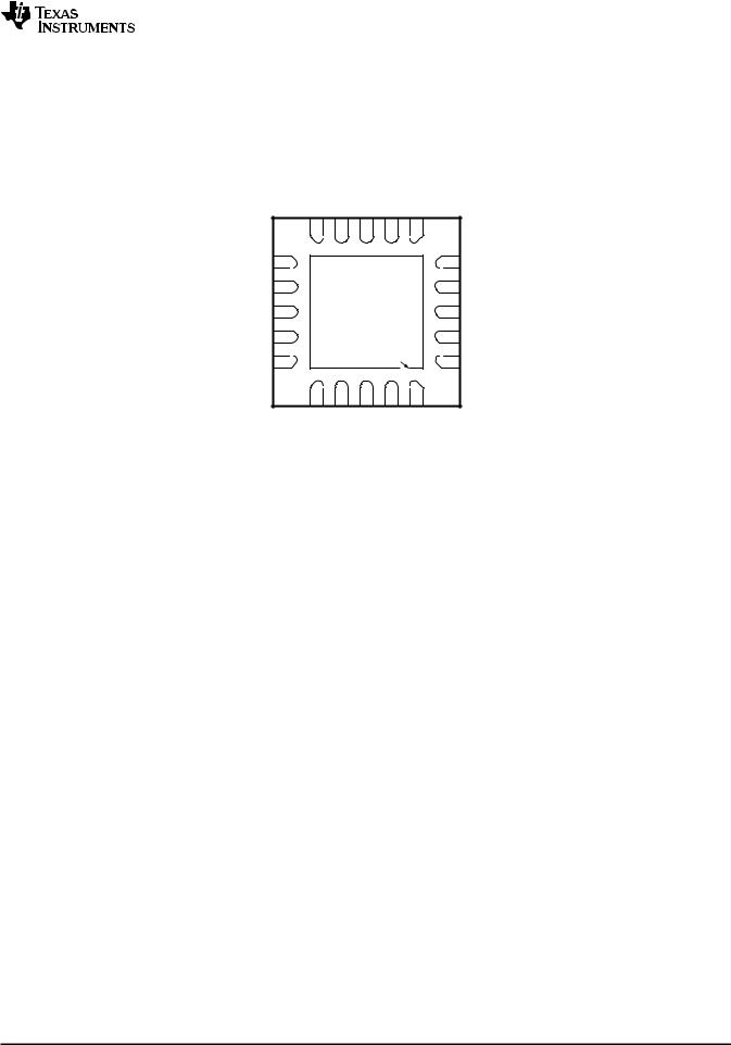
RUK PACKAGE
20 PINS
(TOP VIEW)
|
EN1 |
VCLK |
SW1 |
VBST1 |
DRVH1 |
|
|
|
20 |
19 |
18 |
17 |
16 |
|
|
CS1 |
1 |
|
|
|
15 |
DRVL1 |
|
VFB1 |
2 |
|
|
|
14 |
VO1 |
|
VREG3 |
3 |
TPS51225 |
13 |
VREG5 |
|||
TPS51225B |
|||||||
|
|
|
|
||||
|
|
TPS51225C |
|
|
|||
VFB2 |
4 |
|
|
|
12 |
VIN |
|
CS2 |
5 |
Thermal Pad |
11 |
DRVL2 |
|||
|
6 |
7 |
8 |
9 |
10 |
|
|
|
EN2 |
PGOOD |
SW2 |
VBST2 |
DRVH2 |
|
|
|
|
|
PIN FUNCTIONS |
|
|
PIN NO. |
|
|
|
|
|
|
|
|
NAME |
TPS51225 |
I/O |
DESCRIPTION |
|
TPS51225B |
||||
|
|
|
||
|
TPS51225C |
|
|
|
|
|
|
|
|
CS1 |
1 |
O |
Sets the channel 1 OCL trip level. |
|
|
|
|
|
|
CS2 |
5 |
O |
Sets the channel 2OCL trip level. |
|
|
|
|
|
|
DRVH1 |
16 |
O |
High-side driver output |
|
|
|
|
|
|
DRVH2 |
10 |
O |
High-side driver output |
|
|
|
|
|
|
DRVL1 |
15 |
O |
Low-side driver output |
|
|
|
|
|
|
DRVL2 |
11 |
O |
Low-side driver output |
|
|
|
|
|
|
EN1 |
20 |
I |
Channel 1 enable. |
|
|
|
|
|
|
EN2 |
6 |
I |
Channel 2 enable. |
|
|
|
|
|
|
PGOOD |
7 |
O |
Power good output flag. Open drain output. Pull up to external rail via a resistor |
|
|
|
|
|
|
SW1 |
18 |
O |
Switch-node connection. |
|
|
|
|
|
|
SW2 |
8 |
O |
Switch-node connection. |
|
|
|
|
|
|
VBST1 |
17 |
I |
Supply input for high-side MOSFET (bootstrap terminal). Connect capacitor from this pin to SW |
|
VBST2 |
9 |
I |
terminal. |
|
|
|
|
|
|
VCLK |
19 |
O |
Clock output for charge pump. |
|
|
|
|
|
|
VFB1 |
2 |
I |
Voltage feedback Input |
|
|
|
|
||
VFB2 |
4 |
I |
||
|
||||
|
|
|
|
|
VIN |
12 |
I |
Power conversion voltage input. Apply the same voltage as drain voltage of high-side MOSFETs of |
|
channel 1 and channel 2. |
||||
|
|
|
||
VO1 |
14 |
I |
Output voltage input, 5-V input for switch-over. |
|
|
|
|
|
|
VREG3 |
3 |
O |
3.3-V LDO output. |
|
|
|
|
|
|
VREG5 |
13 |
O |
5-V LDO output. |
|
|
|
|
|
|
Thermal |
— |
— |
GND terminal, solder to the ground plane |
|
pad |
||||
|
|
|
||
|
|
|
|
Copyright © 2012, Texas Instruments Incorporated |
Submit Documentation Feedback |
7 |
Product Folder Links :TPS51225 TPS51225B TPS51225C
TPS51225, TPS51225B, TPS51225C
SLUSAV0B –JANUARY 2012 –REVISED SEPTEMBER 2012 |
www.ti.com |
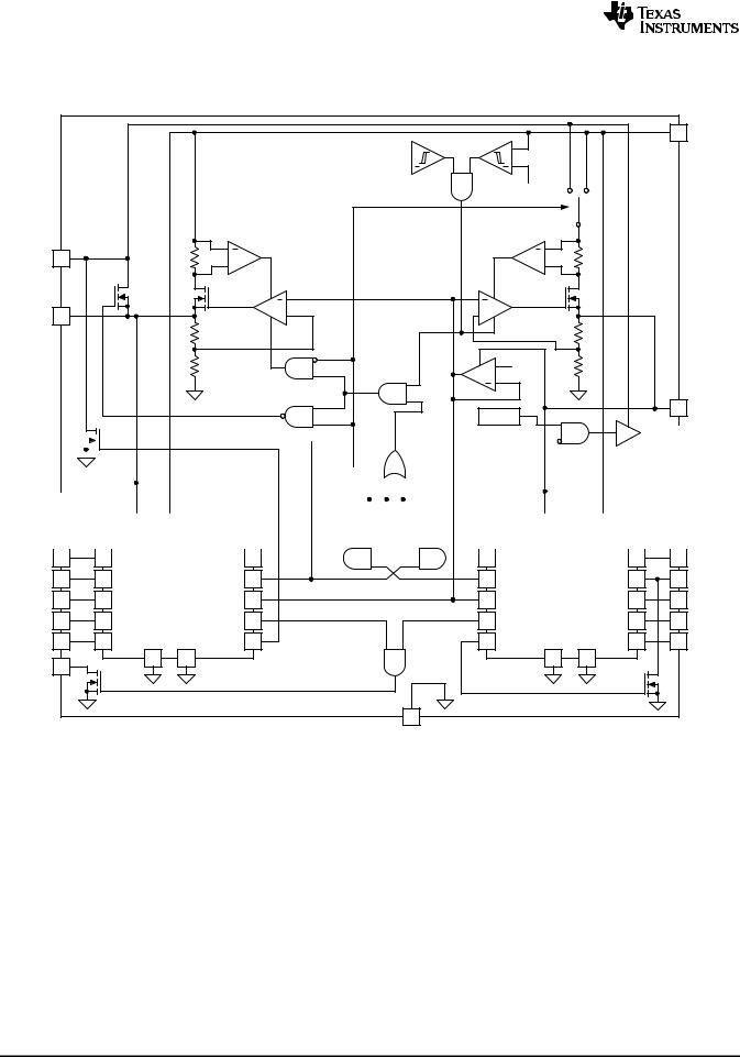
FUNCTIONAL BLOCK DIAGRAM (TPS51225/B/C)
VO 1
VREG 5
EN1
VBST1 DRVH 1
SW 1
DRVL 1 VFB1 CS1
PGOOD
TPS51225
TPS51225B
TPS51225C |
+ |
+ |
155°C/145°C
4.5 V/4.0 V
+ |
|
+ |
+ |
+ |
|
|
+ |
2 V |
|
Osc |
|
|
|
|
|
|
|
|
|
|
|
|
|
|
|
|
|
|
|
|
|
|
|
|
|
|
|
|
|
|
|
|
|
|
|
|
|
|
|
|
|
|
|
|
|
|
|
|
|
|
|
|
|
|
|
|
|
|
|
|
|
|
|
|
|
|
|
|
|
|
|
|
|
|
|
|
|
|
|
|
|
|
|
|
|
|
|
|
|
|
|
|
|
|
|
|
|
|
|
|
|
|
|
|
|
|
|
|
|
|
|
|
|
|
|
|
|
|
|
|
|
|
|
|
|
|
|
|
|
|
|
|
|
|
|
|
|
|
|
|
|
|
|
|
|
|
|
|
|
|
|
|
|
|
|
|
|
|
|
|
|
|
|
|
|
|
|
|
|
|
|
|
|
|
|
|
|
|
|
|
|
|
|
|
|
|
|
|
|
|
|
|
|
|
|
|
|
|
|
|
|
|
|
|
|
|
|
|
|
|
|
|
|
|
|
|
|
|
|
|
|
|
|
|
|
|
|
|
|
|
|
|
|
|
|
|
|
|
|
|
|
|
|
|
|
|
|
|
|
|
|
|
|
|
|
|
|
|
|
|
|
|
|
|
|
|
|
|
|
|
|
|
|
|
|
|
|
|
|
|
|
|
|
|
|
|
|
|
|
|
|
|
|
|
|
|
|
|
|
|
|
|
|
|
|
|
|
|
|
|
|
|
|
|
|
|
|
|
|
|
|
|
|
|
|
|
|
|
|
|
|
|
|
|
|
|
|
|
|
|
|
|
|
|
|
|
|
|
|
|
|
|
|
|
|
|
|
|
|
|
|
|
|
|
|
|
|
|
|
|
|
|
|
|
|
|
|
|
|
|
|
|
|
|
|
|
|
|
|
|
|
|
|
|
|
|
|
|
|
|
|
|
|
|
|
|
|
|
|
|
|
|
|
|
|
|
|
|
|
|
|
|
|
|
|
|
|
|
|
|
|
|
|
|
|
|
|
|
|
|
|
|
|
|
|
|
|
|
|
|
|
|
|
|
|
|
|
|
|
|
|
|
|
|
|
|
|
|
|
|
|
|
|
|
|
|
|
|
VDRV VIN VDD VO_OK |
|
|
|
|
|
|
|
|
|
|
|
|
|
|
VDD VDRV VIN |
|
|
|
|
|
|||||||||||||||||||
|
|
|
|
|
|
|
|
|
|
|
|
|
|
|
|
|
|
|
|
|
|
|
|
|
|
|
|
|||||||||||||||||||
|
|
|
|
|
|
|
|
|
|
|
|
|
|
|
|
|
|
|
|
|
|
|
|
|
|
|
|
|
|
|
|
|
|
|
|
|
|
|
|
|
|
|
|
|
|
|
|
|
|
|
|
|
|
|
|
|
|
|
|
|
|
EN |
|
|
|
|
|
|
|
|
|
|
|
EN |
|
|
|||||||||||||||||
|
|
|
|
|
|
|
|
|
|
|
|
|
|
|
|
|
|
|
|
|
|
|
|
|
|
|||||||||||||||||||||
Switcher |
FAULT |
FAULT |
Switcher |
||
|
|
|
|
||
Controller |
|
|
Controller |
||
(CH1) |
REF |
REF |
(CH2) |
|
|
|
|
PGOOD |
PGOOD |
|
|
PGND |
GND |
DCHG |
DCHG |
GND |
PGND |
|
|
|
GND |
|
|
|
|
|
(Thermal Pad ) |
|
|
VIN
VREG 3
VCLK
EN2
VBST 2 DRVH 2
SW 2
DRVL 2 VFB2 CS2
UDG-12002
8 |
Submit Documentation Feedback |
Copyright © 2012, Texas Instruments Incorporated |
Product Folder Links :TPS51225 TPS51225B TPS51225C
TPS51225, TPS51225B, TPS51225C
www.ti.com |
SLUSAV0B –JANUARY 2012–REVISED SEPTEMBER 2012 |
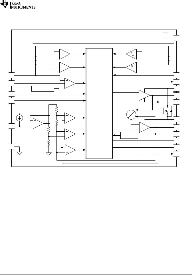
SWITCHER CONTROLLER BLOCK DIAGRAM
|
TPS51225 |
|
|
|
|
VDD |
|
TPS51225B |
|
|
|
|
|
|
|
|
|
|
|
|
|
TPS51225C |
|
|
|
|
|
|
VREF –40% |
+ |
|
|
+ |
VREF +5%/10% |
|
|
UV |
|
|
|
|
|
|
+ |
|
Control Logic |
+ |
|
|
|
OV |
|
|
|
|
|
VREF +15% |
|
|
|
|
VREF –5%/10% |
VFB |
|
|
|
|
|
EN |
REF |
|
|
+ |
PWM |
|
VO_OK |
|
|
|
|
|||
|
|
|
|
|
||
|
SS Ramp Comp |
|
+ |
|
|
VBST |
|
|
|
|
|
||
SKIP |
|
|
|
|
HS |
DRVH |
|
|
|
|
|
||
VIN |
|
|
|
|
|
SW |
|
|
|
|
|
|
|
|
|
|
|
|
XCON |
|
|
|
|
OC |
|
|
VDRV |
|
|
|
+ |
|
|
|
|
10 µA |
|
|
|
|
|
|
|
|
|
|
|
|
CS |
+ |
|
|
|
LS |
DRVL |
|
|
|
|
|
||
|
|
|
NOC |
|
One-Shot |
PGND |
|
|
|
+ |
|
|
|
|
|
|
|
|
|
|
|
|
|
|
Discharge |
|
DCHG |
GND |
|
|
+ |
PGOOD |
|
PGOOD |
|
|
|
ZC |
|
|
|
|
|
|
|
|
|
FAULT |
|
|
|
|
|
|
UDG-12007 |
Copyright © 2012, Texas Instruments Incorporated |
Submit Documentation Feedback |
9 |
Product Folder Links :TPS51225 TPS51225B TPS51225C

TPS51225, TPS51225B, TPS51225C
SLUSAV0B –JANUARY 2012 –REVISED SEPTEMBER 2012 |
www.ti.com |
DETAILED DESCRIPTION
PWM Operations
The main control loop of the switch mode power supply (SMPS) is designed as an adaptive on-time pulse width modulation (PWM) controller. It supports a proprietary D-CAP™ mode. D-CAP™ mode does not require external conpensation circuit and is suitable for low external component count configuration when used with appropriate amount of ESR at the output capacitor(s).
At the beginning of each cycle, the synchronous high-side MOSFET is turned on, or enters the ON state. This MOSFET is turned off, or enters the ‘OFF state, after the internal, one-shot timer expires. The MOSFET is turned on again when the feedback point voltage, VVFB, decreased to match the internal 2-V reference. The inductor current information is also monitored and should be below the overcurrent threshold to initiate this new cycle. By repeating the operation in this manner, the controller regulates the output voltage. The synchronous low-side (rectifying) MOSFET is turned on at the beginning of each OFF state to maintain a minimum of conduction loss. The low-side MOSFET is turned off before the high-side MOSFET turns on at next switching cycle or when inductor current information detects zero level. This enables seamless transition to the reduced frequency operation during light-load conditions so that high efficiency is maintained over a broad range of load current.
Adaptive On-Time/ PWM Frequency Control
Bacause the TPS51225/B/C does not have a dedicated oscillator for control loop on board, switching cycle is controlled by the adaptive on-time circuit. The on-time is controlled to meet the target switching frequency by feed-forwarding the input and output voltage into the on-time one-shot timer. The target switching frequency is varied according to the input voltage to achieve higher duty operation for lower input voltage application. The switching frequency of CH1 (5-V output) is 300 kHz during continuous conduction mode (CCM) operation when VIN = 20 V. The CH2 (3.3-V output) is 355 kHz during CCM when VIN = 20 V.
Light Load Condition in Auto-Skip Operation (TPS51225/C)
The TPS51225/C automatically reduces switching frequency during light-load conditions to maintain high efficiency. This reduction of frequency is achieved smoothly and without an increase in output voltage ripple. A more detailed description of this operation is as follows. As the output current decreases from heavy-load condition, the inductor current is also reduced and eventually approaches valley zero current, which is the boundary between continuous conduction mode and discontinuous conduction mode. The rectifying MOSFET is turned off when this zero inductor current is detected. As the load current further decreases, the converter runs in discontinuous conduction mode and it takes longer and longer to discharge the output capacitor to the level that requires the next ON cycle. The ON time is maintained the same as that in the heavy-load condition. In reverse, when the output current increase from light load to heavy load, the switching frequency increases to the preset value as the inductor current reaches to the continuous conduction. The transition load point to the light load operation IOUT(LL) (i.e. the threshold between continuous and discontinuous conduction mode) can be calculated as shown in Equation 1.
IOUT(LL ) |
1 |
|
(VIN - VOUT )´ VOUT |
|
|
= |
|
´ |
|
|
|
2 ´ L ´ fSW |
VIN |
|
|||
|
|
|
|
||
where |
|
|
|
|
|
• fSW is the PWM switching frequency |
(1) |
||||
Switching frequency versus output current during light-load conditions is a function of inductance (L), input voltage (VIN) and output voltage (VOUT), but it decreases almost proportional to the output current from the
IOUT(LL).
10 |
Submit Documentation Feedback |
Copyright © 2012, Texas Instruments Incorporated |
Product Folder Links :TPS51225 TPS51225B TPS51225C
Loading...