


Texas Instruments DV2056VL, DV2056TL, DV2056L, BQ2056VSNTR, BQ2056VSN Datasheet
...
bq2056/T/V
Low-Dropout Li-Ion Charge-Control ICs with AutoComp™ Charge-Rate Compensation
Features
Significant reduction in charge time with AutoComp charge-rate compensation
Ideal for low-dropout linear regulator design
1-cell, 2-cell, and programmable multicell versions
Low-cost charger implementation with minimum number of external components
Programmable current limit to accommodate any battery size
Interface to external trickle charger for reviving deeply discharged batteries
High-accuracy charge control
Sleep mode for low power consumption
Direct battery voltage sense without resistive dividers (bq2056 and bq2056T)
Small 8-pin SOIC package
General Description
The bq2056 series ICs are low-cost precision linear charge-control devices for Li-Ion batteries. With a minimum number of external components, the bq2056 is a complete lowdropout linear charger. The dropout voltage is typically less than 0.5V when the bq2056 is used with an external PNP transistor or P-channel FET. Features include proprietary
automatic charge-rate compensation (AutoComp) and a trickle-charger interface output for reviving deeply discharged cells. The bq2056 supports a single-cell 4.1V pack and the 2056T supports a two-cell 8.2V pack. The bq2056V may be externally programmed for supporting other voltages. All versions feature a sleep mode for low-power applications.
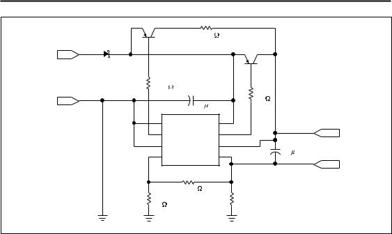
Functional Block Diagram
|
+ |
|
SNS |
TRKL |
|
2.0V |
||
|
BAT
KCOMP
COMP
+
VREG |
CC |
SNS  100mV +
VSS
INH
BDbq2056.eps
Pin Connections |
|
Pin Names |
|
|
||||
|
|
|
|
|
INH |
Charge-inhibit input |
SNS |
Current sense input |
|
|
|
|
|
||||
INH |
1 |
8 |
|
VCC |
TRKL |
Trickle-charge |
BAT |
Battery voltage input |
TRKL |
2 |
7 |
|
CC |
|
interface output |
CC |
Charge control |
|
|
|
||||||
VSS |
3 |
6 |
|
BAT |
VSS |
Ground |
|
output |
|
|
|
|
|
||||
COMP |
4 |
5 |
|
SNS |
COMP |
Charge-rate |
VCC |
Supply input |
|
|
compensation input |
|
|
||||
|
|
|
|
|
|
|
|
|
|
|
|
|
|
|
|
||
8-Pin DIP or Narrow SOIC |
|
|
|
|
||||
|
|
PN-205601.eps |
|
|
|
|
||
|
|
|
|
|
|
|
|
10/98 B |
|
|
|
|
|
|
|
|
|
1

bq2056/T/V
Pin Descriptions:
INH |
Charge-inhibit input |
|
When input to this pin is high, the bq2056 |
|
suspends the charge in progress and places |
|
the device in sleep mode. When input is low, |
|
the bq2056 resumes operation. |
TRKL |
Trickle-charge interface output |
|
This output is driven low if the battery volt- |
|
age is less than an internal threshold level |
|
and INH is low. This open-drain output can |
|
enable an external trickle charger to revive a |
|
deeply discharged battery. |
VSS |
Ground |
COMP |
Charge-rate compensation input |
|
This input is used to set the charge-rate |
|
compensation level. The voltage regulation |
|
output may be programmed to vary as a |
|
function of the charge current delivered to |
|
the battery. This feature, called AutoComp, |
|
provides compensation for internal cell im- |
|
pedance and voltage drops in protection |
|
circuitry and therefore may be used to |
|
safely reduce charging time. Connecting |
|
this pin to VSS disables the AutoComp fea- |
|
ture. |
SNS |
Current sense input |
Battery current is sensed via the voltage developed on this pin by an external senseresistor, connected in series with the negative terminal of the battery pack.
BAT |
Battery voltage input |
This is the battery voltage sense input. It is tied directly to the positive side of the battery pack on bq2056 and bq2056T versions. A simple resistive divider is required to generate this input for bq2056V.
CCCharge-control output
CC is an open-collector output that is used to control the charging current to the battery.
VCC |
VCC supply input |
2
bq2056/T/V
|
Q1 |
|
R3 |
|
|
|
|
|
|
|
|
|
2N3906 |
4.7K |
|
|
|
5 VDC |
|
|
2TX788B |
||
D1 |
|
|
|
||
DC+ |
|
|
|
|
Q2 |
1N5817 |
|
|
|
|
|
|
|
|
|
|
|
|
R5 |
|
|
|
|
|
2.7K |
C2 |
|
R5 |
|
|
|
|
|
||
DC- |
|
|
|
2K |
|
|
|
0.1 F |
|
||
|
|
|
|
||
|
|
|
|
|
|
|
1 |
INH |
VCC |
8 |
|
|
2 |
TRKL |
CC |
7 |
BAT+ |
|
3 |
VS |
BAT |
6 |
C1 |
|
4 |
COMP |
SNS |
5 |
10 F |
|
|
|
10V |
||
|
|
bq2056 |
|
BAT- |
|
|
|
|
|
||
|
|
R2 1K |
|
R6 |
|
|
R1 |
|
|
|
|
|
1K |
|
|
|
0.3 |
bq2056sc.eps
Figure 1. Low-Dropout Single-Cell Li-Ion Charger
Functional Description
The bq2056 supports a precision currentand voltagelimited charging system for Li-Ion batteries. The no-load voltage regulation references (VREG) for the bq2056 and bq2056T are maintained at 4.1V and 8.2V, respectively. The bq2056V provides variable regulation to accommodate a wide range of charge voltages and may be used to meet tighter tolerance requirements through external trimming. The functional block diagram for the bq2056 is on the first page of this data sheet, and Figure 1 illustrates a typical application.
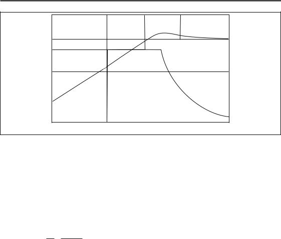
Charge Algorithm
The bq2056 completes the charge cycle in two phases. A constant current phase replenishes approximately 70% of battery capacity, while an accurate voltage regulation phase completes the charge.
Figure 2 shows a typical charge algorithm for bq2056, including charge qualification, current regulation, and voltage regulation phases.
Charge Qualification
During charge qualification the bq2056 detects a low battery and reports this status on pin TRKL. Detection
is accomplished by comparing pin BAT voltage to the internal threshold VMIN. While pin BAT voltage is less than VMIN and pin INH is low, the open-drain output TRKL is driven low and the voltage/current regulator is disabled (CC=high-Z). In the bq2056V, low-voltage detection occurs when the voltage on pin BAT is less than or equal to VMIND. As shown in Figure 1, TRKL enables an external trickle-charge circuit to bring the battery voltage up to VMIN or VMIND.
Current Regulation
The bq2056 provides current regulation while the pack voltage is below the voltage limit. Charge-current feedback, applied through pin SNS, maintains regulation around a threshold of VSNS. The following formula calculates the value of the sense-resistor connected in series with the negative terminal of the battery pack (Figure 3):
RSNS= 0.1/ IMAX
where IMAX is the maximum charging current. IMAX should not exceed 1A.
An external PNP or power P-FET may be used as the series pass element with control provided through output pin CC.
3
bq2056/T/V
Current
External |
AutoComp™ |
|
Trickle Charge |
||
Phase |
||
Enabled |
||
|
||
|
VREG |
|
|
Voltage |
|
IMAX |
Voltage Regulation |
|
|
||
|
VMIN |
|
|
Current |
|
|
Regulation |
Current
Voltage
2056chg.eps
Figure 2. bq2056 Charge Algorithm
Voltage Regulation
Voltage regulation feedback is through pin BAT. This pin is connected directly to the pack in the bq2056 and bq2056T. This voltage is compared with the voltage regulation reference, VREG. In the bq2056V, a resistive divider may be used to generate this input (Figure 4). In this case, the voltage presented on pin BAT is compared with the internal reference voltage VREF. The resistor values RB1 and RB2 (Figure 4) are calculated based on the following equation:
RB1 = N VCELL −
1
RB2 VREF
where
N |
= Number of cells in series |
VCELL = Manufacturer-specified charging voltage
Automatic Charge-Rate Compensation
(AutoComp) Feature
To reduce charging time, the bq2056 series uses the proprietary AutoComp technique to compensate safely for internal impedance of battery and any voltage drops in the protection circuitry. This maximizes battery’s capacity while reducing charging time. Compensation is through input pin COMP (Figure 5). A portion of the current-sense voltage, presented through this pin, is scaled by a factor of KCOMP and summed with the regulation reference, VREG. This process increases the output
voltage to compensate for the battery’s internal impedance and undesired voltage drops in the circuit.
For bq2056 and bq2056T, the voltage across the battery pack, VPAK, is
VPAK = VREG + (KCOMP voltage on pin COMP)
For bq2056V, the compensation voltage is added to the product of the internal voltage reference, VREF, and the gain, KDIV, of the external resistive divider between the battery pack and BAT input, (Figure 4).
VPAK = (VREF KDIV) + (KCOMP voltage on pin COMP)
Sleep Mode
The charge function may be disabled through pin INH. When INH is driven high, internal current consumption is reduced, and pins CC and TRKL assumes a highimpedance output state.
4
 Loading...