


bq2954
Lithium Ion Charge Management IC with Integrated Switching Controller
Features
Safe charge of Li-Ion battery packs
Pulse-width modulation control for current and voltage regulation
Programmable high-side/low-side current-sense
Fast charge terminated by selectable minimum current; safety backup termination at maximum time
Pre-charge qualification detects shorted or damaged cells and conditions battery
Charging continuously qualified by temperature and voltage limits
Direct LED control outputs to display charge status and fault conditions
General Description
The bq2954 Li-Ion Charge-Manage- ment IC uses a flexible pulse-width modulation regulator to control voltage and current during charging. The regulator frequency is set by an external capacitor for design flexibility. The switch-mode design minimizes power dissipation.
For safety, the bq2954 inhibits fast charging until the battery voltage and temperature are within configured limits. If the battery voltage is less than the low-voltage threshold, the bq2954 provides low-current conditioning of the battery.
For charge qualifiction, the bq2954 uses an external thermistor to measure battery temperature. Charging begins when power is applied or the battery is inserted
The bq2954 charges a battery in two phases. First a constant-current phase replenishes approximately 70% of battery capacity. Then a volt- age-regulation phase completes the battery charge.
The bq2954 provides status indications of all charger states and faults for accurate determination of the battery and charge-system conditions.
Pin Connections |
|
Pin Names |
|
|
||||
|
|
|
|
|
TM |
Time-out programming |
TPWM |
Regulator timebase input |
|
|
|
|
|
||||
|
|
|
|
|
|
input |
BTST |
Battery test output |
|
|
|
|
|
CHG |
Charge active output |
||
TM |
1 |
16 |
|
LED2/DSEL |
||||
|
LCOM |
Common LED output |
||||||
|
|
|
||||||
CHG |
2 |
15 |
|
LED1/CSEL |
BAT |
Battery voltage input |
VSS |
System ground |
|
|
|
||||||
|
|
|
|
|
|
|
||
BAT |
3 |
14 |
|
MOD |
VCOMP |
Voltage loop comp input |
VCC |
5.0V±10% power |
|
|
|
|
|
|
|
||
VCOMP |
4 |
13 |
|
VCC |
ICOMP |
Current loop comp input |
MOD |
Modulation control |
ICOMP |
5 |
12 |
|
VSS |
|
|
||
|
ITERM |
Minimum current |
|
output |
||||
ITERM |
6 |
11 |
|
LCOM |
|
termination select input |
LED1/ |
Charge status output 1/ |
|
|
|
||||||
SNS |
7 |
10 |
|
BTST |
SNS |
Sense resistor input |
CSEL |
Charge sense select |
|
|
|
|
|
|
|
|
input |
TS |
8 |
9 |
|
TPWM |
TS |
Temperature sense input |
LED2/ |
Charge status output 2/ |
|
|
|
|
|
|
|
||
|
16-Pin Narrow |
|
|
|
DSEL |
Display select input |
||
|
|
|
|
|
|
|||
|
DIP or SOIC |
|
|
|
|
|
||
|
|
|
PN295401.eps |
|
|
|
|
|
|
|
|
|
|
|
|||
SLUS064–OCTOBER 1998 B |
|
|
|
|
|
|||
1

bq2954
Pin Descriptions
TM |
Time-out programming input |
|
Sets the maximum charge time. The resistor |
|
and capacitor values are determined using |
|
Equation 5. Figure 10 shows the resistor/ca- |
|
pacitor connection. |
CHG |
Charge active output |
|
An open-drain output is driven low when the |
|
battery is removed, during a temperature |
|
pend, when a fault condition is present, or |
|
when charge is done. CHG can be used to |
|
disable a high-value load capacitor to detect |
|
quickly any battery removal. |
BAT |
Battery voltage input |
|
Sense input. This potential is generally de- |
|
veloped using a high-impedance resistor di- |
|
vider network connected between the posi- |
|
tive and the negative terminals of the bat- |
|
tery. See Figures 6 and 7 and Equation 1. |
VCOMP |
Voltage loop compensation input |
|
Connects to an external R-C network to sta- |
|
bilize the regulated voltage. |
ICOMP |
Current loop compensation input |
|
Connects to an external R-C network to sta- |
|
bilize the regulated current. |
ITERM |
Charge full and minimum current termi- |
|
nation select |
|
Three-state input is used to set IFULL and |
|
IMIN for fast charge termination. See Table 4. |
SNS |
Charging current sense input |
|
Battery current is sensed via the voltage devel- |
|
oped on this pin by an external sense-resistor. |
TS |
Temperature sense input |
|
Used to monitor battery temperature. An exter- |
|
nal resistor-divider network sets the lower and |
|
upper temperature thresholds. (See Figures 8 |
|
and 9 and Equations 3 and 4.) |
TPWM |
Regulation timebase input |
|
Uses an external timing capacitor to ground |
|
to set the pulse-width modulation (PWM) |
|
frequency. See Equation 7. |
BTST |
Battery test output |
|
Driven high in the absence of a battery in or- |
|
der to provide a potential at the battery ter- |
|
minal when no battery is present. |
LCOM |
Common LED output |
|
Common output for LED1-2. This output is |
|
in a high-impedance state during initiali- |
|
zation to read programming input on DSEL |
|
and CSEL. |
VSS |
Ground |
VCC |
VCC supply |
|
5.0V, ±10% |
MOD |
Current-switching control output |
|
Pulse-width modulated push/pull output used |
|
to control the charging current to the battery. |
|
MOD switches high to enable current flow and |
|
low to inhibit current flow. (The maximum |
|
duty cycle is 80%.) |
LED1– |
Charger display status 1–2 outputs |
LED2 |
Drivers for the direct drive of the LED dis- |
|
|
|
play. These outputs are tri-stated during |
|
initialization so that DSEL and CSEL can be |
|
read. |
DSEL |
Display select input (shared pin with |
|
LED2) |
|
Three-level input that controls the LED1–2 |
|
charge display modes. |
CSEL |
Charge sense-select input (shared pin |
|
with LED1) |
|
Input that controls whether current is |
|
sensed on low side of battery or high side of |
|
battery. A current mirror is required for |
|
high-side sense. |
2
bq2954
VCC |
TM |
ITERM |
TPWM |
|
Power-On |
MTO |
|
Oscillator |
|
Reset |
Timer |
|
|
|
|
|
|
||
VSS |
|
|
DSEL |
|
|
|
CSEL |
|
|
Voltage |
|
Charge |
Display |
LED1 |
|
Control |
LED2 |
||
Reference |
|
Control |
||
|
|
State |
|
BTST |
TS |
|
Machine |
|
CHG |
|
|
|
||
|
|
|
|
|
VCOMP |
|
|
|
LCOM |
|
|
|
|
|
BAT |
|
|
|
|
SNS |
|
PWM |
|
MOD |
|
|
Regulator |
|
|
|
|
|
|
|
ICOMP |
|
|
|
BD2954.eps |
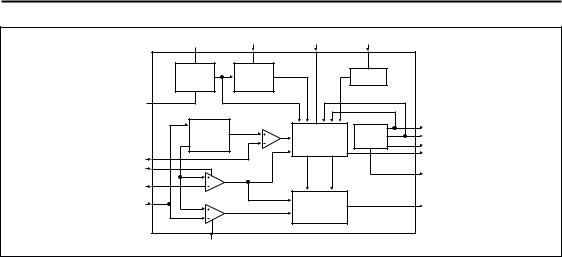
Figure 1. Functional Block Diagram
Functional Description
The bq2954 functional operation is described in terms of the following (Figure 1):
■Charge algorithm
■Charge qualification
■Charge status display
■Configuring the display and termination
■Voltage and current monitoring
■Battery insertion and removal
■Temperature monitoring
■Maximum time--out
■Charge regulation
■Recharge after fast charge
Charge Algorithm
The bq2954 uses a two-phase fast-charge algorithm. In phase 1, the bq2954 regulates constant current until the voltage on the BAT pin, VBAT, rises to the internal threshold, VREG. The bq2954 then transitions to phase 2 and regulates constant voltage (VBAT = VREG) until the charging current falls below the programmed IMIN threshold. Fast charge then terminates, and the bq2954 enters the Charge Complete state. (See Figure 2.)
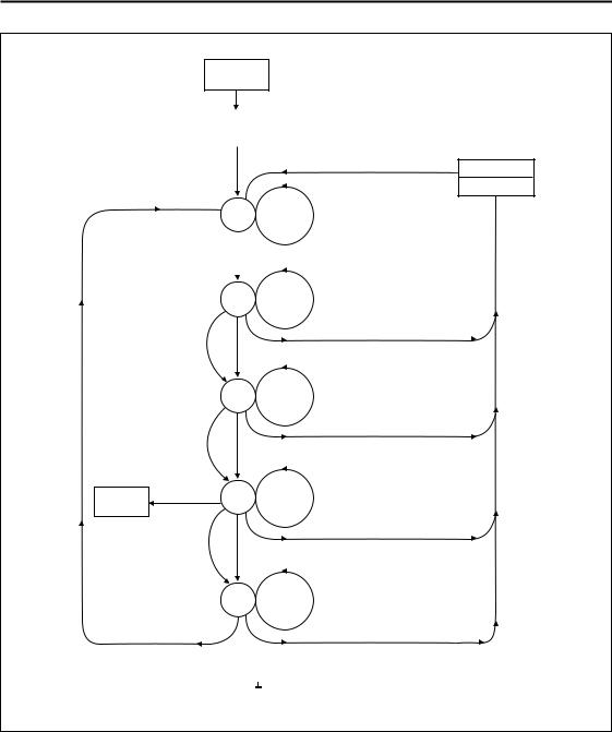
Charge Qualification
The bq2954 starts a charge cycle when power is applied while a battery is present or when a battery is inserted. Figure 2 shows the state diagram for the bq2954. The bq2954 first checks that the battery temperature is within the allowed, user-configurable range. If the temperature is out of range, the bq2954 remains in the QUALIFICATION state (S01) and waits until the battery temperature and voltage are within the allowed range.
If during any state of charge, a temperature excursion occurs HOT, the bq2954 proceeds to the DONE state (S04) and indicates this state on the LED outputs and provides no current. If this occurs, the bq2954 remains in the DONE state unless the following two conditions are met:
■Temperature falls within valid charge range
■VBAT falls below the internal threshold,VRCHG
If these two conditions are met, a new charge cycle begins. During any state of charge, if a temperature excursion occurs COLD, the bq2954 terminates charge and returns to the QUALIFICATION state (S01). Charge restarts if VBAT and temperature are in valid range.
When the temperature and voltage are valid, the bq2954 enters the CONDITIONING state (S02) and regulates current to ICOND (=IMAX/10). After an initial holdoff period tHO (which prevents the IC from reacting to transient voltage spikes that may occur when charge current is first applied), the IC begins monitoring VBAT. If VBAT does not rise to at least VMIN before the expiration of
3
bq2954
Volt Fault: When VBAT > VHCO
VCC "Up" Time Fault: When T = MTO/4 in State S02 or T = MTO in S03a
Hold Time: A VHCO Fault or State charge held off for 0.740s to 1.12s
Mod = 0 |
Power-On |
No Action |
|
Reset |
|||
|
|
||
|
|
|
|
|
Latch DSEL/CSEL Inputs |
||
Battery Removal
VBAT < 0.8V Reset Faults
Latch DSEL/CSEL Inputs
VBAT< VRCHG |
|
|
Temp Not Valid |
|
|
|
0.8V > VBAT > VHCO |
||
|
S01 |
Hold Time |
||
QUALIFICATION |
Hold-off Faults |
|||
|
|
|||
|
|
CHG = 0 |
||
|
|
|
||
|
|
|
Battst = 1 |
|
|
|
|
Temp Valid |
|
|
|
|
VHCO < VBAT >0.8V |
|
|
|
|
Reset MTO |
|
|
|
|
|
|
CONDITIONING
S02
Temp Not Valid
VBAT >VMIN
Reset MTO
CURRENT S03a
REGULATION
|
Temp Not Valid |
|
VBAT = VREG |
|
VOLTAGE |
Full Charge |
REGULATION S03b |
Indication |
ISNS = IMIN |
VBAT < VMIN: ISNS = IMAX/10 Hold Time
CHG = 1
Time Fault
T = MTO/25
ISNS = IMAX: VBAT<VREG
T< MTO
Hold Time
CHG = 1
Volt or Time Fault
VBAT > VHCO or T = MTO
VBAT = VREG: IMAX > ISNS > ITRMN T< MTO
CHG = 1
Volt Fault
Temp Not Valid
T = MTO
ISNS = ITRM
DONE S04
Temp Not Hot andVBAT<VRCHG
1s Hold Time after VBAT < VRCHG
VBAT Voltages:
VRCHG = 1.92V 0.5V
VMIN = 1.50V 0.5V
0.5V
VBAT > VHCO
Temp Hot
VBAT > VRCHG Hold-off MOD
VRCHG < VBAT < VHCO CHG = 1
Volt Fault
VBAT > VHCO
VREG = 2.05V
VHCO = 2.30V
Fault
CHG = 0
Volt or
Time Fault
FGbg295401.eps
Figure 2. bq2954 Charge Algorithm
4

|
|
|
|
|
|
|
|
|
|
|
bq2954 |
|
|
|
|
|
|
R2 |
|
|
|
|
|
8-24VDC ±10% |
D4 |
|
|
|
4.7K |
|
|
|
L2 |
|
|
|
VDC |
|
|
|
|
|
|
|
|
BAT+ |
|
|
|
|
Q1 |
|
|
|
|
Q5 |
47uH |
||
|
|
|
|
|
|
|
|
|
|||
|
B130DI |
|
FMMT3906 |
|
Q2 |
|
|
||||
|
|
|
|
FZT789A |
|
|
|||||
|
|
|
|
|
R1 |
FMMt3904 |
|
|
|
||
|
|
C10 |
|
|
|
|
D5 |
|
|||
|
|
|
R4 |
|
|
|
|
||||
|
|
47uF |
|
1K |
|
|
|
|
|
||
|
|
|
10K |
|
|
|
|
B130DI |
|
||
|
|
25V |
|
|
|
|
|
|
|
||
|
|
|
|
|
|
|
|
|
|
|
|
|
U2 |
|
|
|
|
|
|
|
|
C11 |
|
|
|
5V |
R5 |
|
|
|
L1 |
|
10uF |
||
|
ZMR500 |
|
|
D1 |
|
|
|
20V |
|||
|
|
|
10K |
|
|
10 uH |
R14 |
||||
|
IN |
G |
OUT |
|
|
|
PCS4106 |
||||
|
|
|
1N4148 |
|
|
||||||
|
|
N |
|
|
|
|
|
|
|
RB1 |
|
|
C3 |
D |
|
C2 |
|
|
|
|
|
|
|
|
|
|
|
|
|
|
|
|
|
||
|
1uF |
|
|
1uF |
Q3 |
|
|
|
|
|
|
|
25V |
|
|
|
|
|
|
|
|
|
|
|
|
|
|
FMMT451 |
|
|
5V |
|
|
|
|
|
|
|
|
|
|
|
|
|
|
||
|
|
|
|
|
|
|
|
|
|
|
|
|
|
|
|
|
|
|
|
|
|
R15 |
|
|
|
|
|
R6 |
|
R9 |
|
|
|
RB2 |
|
|
|
|
|
|
|
|
|
|
|
||
|
|
|
|
10K |
|
220 |
|
|
|
|
BAT- |
|
|
|
|
|
|
|
|
R10 |
|
R8 |
|
|
|
|
|
|
|
|
62K |
|
|
||
|
|
|
|
|
|
|
|
|
|
0.25 5% |
|
|
|
|
|
|
|
|
|
|
C8 |
0.5W |
|
|
|
|
|
|
|
|
|
|
|
|
|
|
D2 |
|
C6 |
|
C4 |
|
|
1000pF |
5V |
|
|
|
|
|
0.1 uF |
|
|
|
R7 |
|
|||
|
GRREN |
|
|
|
|
|
|
|
|||
|
|
|
|
|
|
|
|
|
|
1K |
|
|
|
|
0.1 uF |
16 |
U1 |
|
|
1 |
|
|
|
|
|
|
|
|
|
|
|
|
|||
|
|
|
|
LED2/DSEL |
|
TM |
|
|
|
||
R13 |
|
|
|
15 |
|
2 |
|
|
|
||
D3 |
|
|
LED1/CSEL |
|
CHG |
|
|
|
|||
1K |
|
|
14 |
|
3 |
|
|
|
|||
|
|
MOD |
|
BAT |
|
|
|
||||
RED |
|
|
13 |
|
4 |
|
|
R12 |
|||
|
|
|
VCC |
|
VCOMP |
|
R11 |
||||
|
|
|
|
12 |
|
5 |
|
||||
|
|
|
|
VSS |
|
ICOMP |
|
|
|
||
|
|
|
|
11 |
|
6 |
|
|
|
||
|
|
|
|
LCOM |
|
ITERM |
|
4.32K |
8.45K |
||
|
|
|
|
10 |
|
7 |
|
||||
|
|
|
|
BTST |
|
SNS |
|
1% |
1% |
||
|
|
|
|
9 |
|
8 |
|
||||
|
|
|
R3 |
TPWM |
|
TS |
|
||||
|
|
|
|
|
|
|
|
TEM+ |
|||
|
|
|
10K |
C9 |
bq2954 |
|
|
C7 |
|
|
|
|
|
|
|
|
|
|
|
|
|||
|
|
|
|
|
|
|
C5 |
0.01uF |
|
|
|
|
|
|
|
|
|
|
|
|
|
||
|
|
|
|
470pF |
|
|
0.1uF |
C1 |
|
||
|
Q4 |
|
|
|
|
|
|
|
|
||
|
|
|
|
|
|
|
|
|
0.1uF |
|
|
|
FMMT3904 |
|
|
|
|
|
|
|
|
|
|
|
|
|
|
|
|
|
|
|
|
|
|
|
1. IMAX = 1.0A, Vreg = 4.2V ± 1% PER CELL |
|
|
|
|
|
|
2954sch9/23/98 |
|||
|
|
|
|
|
|
|
|
||||
|
2. MTO = 3 HRS, IFULL = IMAX/5, ITERM = IMAX/10 |
|
|
|
|
|
|
|
|||
|
3. TEMP = 0-45˚C, |
|
|
|
|
|
|
|
|
|
|
|
4. Frequency = 200kHz |
|
|
|
|
|
|
|
|
|
|
Figure 3. High-Efficiency Li-Ion Charger for 1–4 Cells
5
bq2954
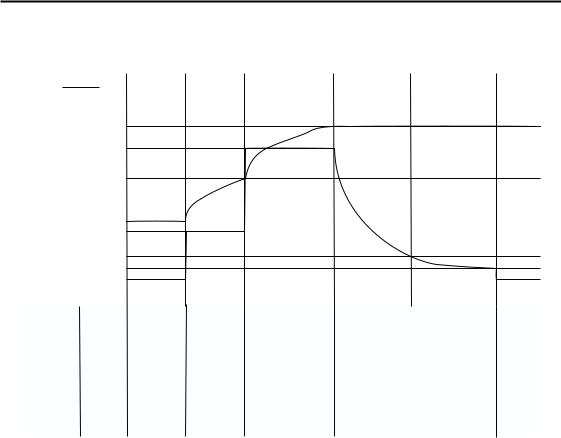
Table 1. Normal Fast Charge Cycle
VBAT |
|
|
Battery |
|
Fast Charge |
Voltage |
IFULL |
|
Charge |
|||
|
|
|
|
|
|
Qualification |
Current |
Regulate |
Detect |
|
||
IBAT |
|
|
|
|
|
|
Complete |
|||||
|
|
|
|
|
Absent |
Regulate |
Current |
|
|
|||
|
|
|
|
|
|
|
|
|||||
|
|
|
|
|
|
|
|
|||||
|
|
|
|
VREG |
|
|
|
Taper |
|
|
|
|
|
|
|
|
|
|
|
|
|
|
|
||
|
|
|
|
IMAX |
|
|
|
|
|
|
|
|
|
|
|
|
VMIN |
|
|
|
|
|
|
|
|
|
|
|
|
ICOND |
|
|
|
|
|
|
|
|
|
|
|
|
IFULL |
|
|
|
|
|
|
|
|
|
|
|
|
IMIN |
|
|
|
|
|
|
|
|
|
|
|
|
|
|
|
|
Time |
|
|
MTO |
|
|
|
|
|
|
|
|
|
|
|
|
|
|
Mode 1 |
LED1 |
Low |
High |
High |
High |
Low |
|
Low |
||||
(DSEL = 0) |
LED2 |
Low |
Low |
Low |
Low |
High |
|
High |
||||
Mode 2 |
LED1 |
Low |
High |
High |
High |
Low |
|
Low |
||||
(DSEL = 1) |
|
LED2 |
Low |
Low |
Low |
Low |
High |
|
High |
|||
Mode 3 |
LED1 |
Low |
High |
High |
High |
Low |
|
Low |
||||
(DSEL = F) |
|
LED2 |
Low |
Low |
Low |
High |
High |
|
High |
|||
Mode 1 |
CHG |
Low |
High |
High |
High |
High |
|
Low |
||||
and 2 |
|
BTST |
High |
Low |
Low |
Low |
Low |
|
Low |
|||
Mode 3 |
|
|
CHG |
Low |
High |
High |
High |
High |
|
Low |
||
|
BTST |
High |
High |
Low |
Low |
Low |
|
Low |
||||
|
|
|
|
|
||||||||
|
|
|
|
|
|
|
|
|
|
|
GR295401.eps |
|
time-out limit tQT (i.e., the battery has failed short), the bq2954 enters the Fault state. Then tQT is set to 25% of tMTO. If VMIN is achieved before expiration of the time limit, the bq2954 begins fast charging.
Once in the Fault state, the bq2954 waits until VCC is cycled or a new battery insertion is detected. It then starts a new charge cycle and begins the qualification process again.
Charge Status Display
Charge status is indicated by the LED driver outputs LED1–LED2. Three display modes (Tables 1– 3) are available in the bq2954 and are selected by configuring pin DSEL. Table 1 illustrates a normal fast charge cycle, Table 2 a recharge-after-fast-charge cycle, and Table 3 an abnormal condition.
Configuring the Display Mode, IFULL/IMIN,
and ISENSE
DSEL/LED2 and CSEL/LED1 are bi-directional pins with two functions: as LED driver pins (output) and as programming pins (input). The selection of pull-up, pull-down, or no-resistor programs the display mode on DSEL as shown in Tables 1 through 3. A pull-down or no-resistor programs the current-sense mode on CSEL.
The bq2954 latches the programming data sensed on the DSEL and CSEL input when VCC rises to a valid level. The LEDs go blank for approximately 400ms (typical) while new programming data are latched.
When fast charge reaches a condition where the charging current drops below IFULL, the LED1 and LED2 outputs indicate a full-battery condition. Fast charge terminates when the charging current drops below the
6
 Loading...