


INA200
IN A 2 0 0 INA201
INA202
SBOS374B − NOVEMBER 2006 − REVISED OCTOBER 2007
High-Side Measurement Current-Shunt Monitor
with Comparator and Reference
FEATURES
DCOMPLETE CURRENT SENSE SOLUTION
D0.6V INTERNAL VOLTAGE REFERENCE
DINTERNAL OPEN-DRAIN COMPARATOR
DLATCHING CAPABILITY ON COMPARATOR
DCOMMON-MODE RANGE: −16V to +80V
DHIGH ACCURACY: 3.5% MAX ERROR OVER TEMPERATURE
DBANDWIDTH: 500kHz (INA200)
DQUIESCENT CURRENT: 1800 A (max)
DPACKAGES: SO-8, MSOP-8
DESCRIPTION
The INA200, INA201, and INA202 are high-side current-shunt monitors with voltage output. The INA200−INA202 can sense drops across shunts at common-mode voltages from −16V to 80V. The INA200−INA202 are available with three output voltage scales: 20V/V, 50V/V, and 100V/V, with up to 500kHz bandwidth.
The INA200, INA201, and INA202 also incorporate an open-drain comparator and internal reference providing a 0.6V threshold. External dividers are used to set the current trip point. The comparator includes a latching capability, which can be made transparent by grounding (or leaving open) the RESET pin.
APPLICATIONS
DNOTEBOOK COMPUTERS
DCELL PHONES
DTELECOM EQUIPMENT
DAUTOMOTIVE
DPOWER MANAGEMENT
DBATTERY CHARGERS
DWELDING EQUIPMENT
The INA200, INA201, and INA202 operate from a single +2.7V to +18V supply, drawing a maximum of 1800 A of supply current. Package options include the very small MSOP-8 and the SO-8. All versions are specified over the extended operating temperature range of −40 °C to +125°C.
|
|
INA200 (G = 20) |
|
|
1 |
|
INA201 (G = 50) |
|
|
V+ |
INA202 (G = 100) |
|
|
|
|
|
|
||
|
|
|
|
|
|
|
|
VIN+ |
8 |
2 |
OUT |
G |
|
|
|
|
VIN− |
7 |
|
|
|
|
||
|
|
0.6V |
|
|
|
|
Reference |
|
|
3 |
CMPIN |
CMPOUT |
6 |
|
|
|
|||
|
|
Comparator |
|
|
4 |
GND |
|
|
|
|
|
|
RESET |
5 |
Please be aware that an important notice concerning availability, standard warranty, and use in critical applications of Texas Instruments semiconductor products and disclaimers thereto appears at the end of this data sheet.
All trademarks are the property of their respective owners.
PRODUCTION DATA information is current as of publication date. Products |
Copyright 2006−2007, T exas Instruments Incorporated |
conform to specifications per the terms of Texas Instruments standard warranty. |
|
Production processing does not necessarily include testing of all parameters. |
|
www.ti.com

INA200
INA201
INA202 |
www.ti.com |
SBOS374B − NOVEMBER 2006 − REVISED OCTOBER 2007 |
|
ABSOLUTE MAXIMUM RATINGS(1)
. . . . . . . . . . . . . . . .Supply Voltage, V+ |
. . . . . . . . . . . . . . . . . . . 18V |
Current-Shunt Monitor Analog Inputs, VIN+, VIN− |
|
Differential (VIN+) − (V IN− ) . . . . . . . . |
. . . . . . . . . . −18V to +18V |
Common Mode(2) . . . . . . . . . . . . . . |
. . . . . . . . . . −16V to +80V |
Comparator Analog Input and Reset Pins(2) . . . . . . . . . . . . . . . . . |
|
. . . . . . . . . . . . . . . . . . . . . . . . . . . . . . . . . |
GND − 0.3V to (V+) + 0.3V |
Analog Output, Out(2) . . . . . . . . . . . . . |
GND − 0.3V to (V+) + 0.3V |
Comparator Output, Out Pin(2) . . . . . . . |
. . . . . . GND − 0.3V to 18V |
Input Current Into Any Pin(2) . . . . . . . . |
. . . . . . . . . . . . . . . . . . 5mA |
Operating Temperature . . . . . . . . . . . . . |
. . . . . . . . −55 °C to +150°C |
Storage Temperature . . . . . . . . . . . . . . . |
. . . . . . . . −65 °C to +150°C |
Junction Temperature . . . . . . . . . . . . . . . |
. . . . . . . . . . . . . . . . +150°C |
ESD Ratings: |
|
Human Body Model (HBM) . . . . . . . |
. . . . . . . . . . . . . . . . 4000V |
Charged Device Model (CDM) . . . . |
. . . . . . . . . . . . . . . . 1000V |
|
|
(1)Stresses above these ratings may cause permanent damage. Exposure to absolute maximum conditions for extended periods may degrade device reliability. These are stress ratings only, and functional operation of the device at these or any other conditions beyond those specified is not supported.
(2)This voltage may exceed the ratings shown if the current at that pin is limited to 5mA.
This integrated circuit can be damaged by ESD. Texas Instruments recommends that all integrated circuits be handled with appropriate precautions. Failure to observe
proper handling and installation procedures can cause damage.
ESD damage can range from subtle performance degradation to complete device failure. Precision integrated circuits may be more susceptible to damage because very small parametric changes could cause the device not to meet its published specifications.
ORDERING INFORMATION(1)
PRODUCT |
GAIN |
PACKAGE-LEAD |
PACKAGE DESIGNATOR |
PACKAGE MARKING |
|
|
|
|
|
|
|
INA200 |
20V/V |
MSOP-8 |
DGK |
BQH |
|
|
|
|
|||
SO-8 |
D |
INA200A |
|||
|
|
||||
|
|
|
|
|
|
INA201 |
50V/V |
MSOP-8 |
DGK |
BQJ |
|
|
|
|
|||
SO-8 |
D |
INA201A |
|||
|
|
||||
|
|
|
|
|
|
INA202 |
100V/V |
MSOP-8 |
DGK |
BQL |
|
|
|
|
|||
SO-8 |
D |
INA202A |
|||
|
|
||||
|
|
|
|
|
(1)For the most current package and ordering information see the Package Option Addendum at the end of this document, or see the TI web site at www.ti.com.
PIN CONFIGURATIONS
TOP VIEW
|
|
INA200−INA202 |
|
|
V+ |
|
|
|
VIN+ |
|
|
|
||
1 |
|
8 |
||
OUT |
|
|
|
VIN− |
2 |
|
7 |
||
CMPIN |
|
|
|
CMPOUT |
3 |
|
6 |
||
|
|
|
|
RESET |
GND |
4 |
|
5 |
|
|
|
|
|
|
|
|
|
|
|
MSOP−8 (DGK)
SO−8 (D)
2

|
INA200 |
|
INA201 |
www.ti.com |
INA202 |
SBOS374B − NOVEMBER 2006 − REVISED OCTOBER 2007
ELECTRICAL CHARACTERISTICS: CURRENT-SHUNT MONITOR
Boldface limits apply over the specified temperature range: TA = −40 °C to +125°C.
At TA = +25°C, VS = +12V, VCM = +12V, VSENSE = 100mV, RL = 10kΩ to GND, RPULL-UP = 5.1kΩ connected from CMPOUT to VS, and CMPIN = GND, unless otherwise noted.
|
|
|
|
|
INA200, INA201, INA202 |
|
|
|
|||
|
|
|
|
|
|
|
|
|
|
||
CURRENT-SHUNT MONITOR |
|
|
|
|
|
|
|
|
|
||
PARAMETERS |
|
|
CONDITIONS |
MIN |
|
TYP |
MAX |
UNITS |
|||
INPUT |
|
|
|
|
|
|
|
|
|
|
|
Full-Scale Sense Input Voltage |
VSENSE |
VSENSE = VIN+ − V IN− |
|
|
0.15 |
(VS − 0.25)/Gain |
V |
||||
|
|
||||||||||
Common-Mode Input Range |
VCM |
|
|
−16 |
|
|
80 |
V |
|||
Common-Mode Rejection |
CMR |
VIN+ = −16V to +80V |
80 |
|
100 |
|
dB |
||||
Over Temperature |
|
VIN+ = +12V to +80V |
100 |
|
123 |
|
dB |
||||
Offset Voltage, RTI(1) |
VOS |
|
|
|
|
±0.5 |
±2.5 |
mV |
|||
+25°C to +125°C |
|
|
|
|
|
|
±3 |
mV |
|||
−40 °C to +25°C |
|
|
|
|
|
|
|
±3.5 |
mV |
||
|
|
|
|
|
|
|
|||||
vs Temperature |
|
dVOS/dT |
|
TMIN to TMAX |
|
|
5 |
|
µV/°C |
||
|
|
|
|
|
|||||||
vs Power Supply |
PSR |
VOUT = 2V, VIN+ = +18V, 2.7V |
|
|
2.5 |
100 |
µV/V |
||||
Input Bias Current, VIN− Pin |
IB |
|
|
|
|
±9 |
±16 |
µA |
|||
OUTPUT (VSENSE ≥ 20mV) |
|
|
|
|
|
|
|
|
|
|
|
Gain: |
|
G |
|
|
|
|
|
|
|
|
|
INA200 |
|
|
|
|
|
|
20 |
|
V/V |
||
INA201 |
|
|
|
|
|
|
50 |
|
V/V |
||
INA202 |
|
|
|
|
|
|
100 |
|
V/V |
||
Gain Error |
|
|
VSENSE = 20mV to 100mV |
|
|
±0.2 |
±1 |
% |
|
||
Over Temperature |
|
VSENSE = 20mV to 100mV |
|
|
|
±2 |
% |
|
|||
Total Output Error(2) |
|
VSENSE = 120mV, VS = +16V |
|
|
±0.75 |
±2.2 |
% |
|
|||
Over Temperature |
|
VSENSE = 120mV, VS = +16V |
|
|
±0.002 |
±3.5 |
% |
|
|||
Nonlinearity Error(3) |
|
VSENSE = 20mV to 100mV |
|
|
|
% |
|
||||
Output Impedance |
|
RO |
|
|
|
|
1.5 |
|
Ω |
||
Maximum Capacitive Load |
|
No Sustained Oscillation |
|
|
10 |
|
nF |
||||
|
|
|
|
|
|
|
|
|
|
|
|
OUTPUT (V |
< 20mV)(4) |
|
|
|
|
|
|
|
|
|
|
SENSE |
|
|
|
|
|
|
|
|
|
|
|
INA200, INA201, INA202 |
|
−16V ≤ VCM < 0V |
|
|
300 |
|
mV |
||||
INA200 |
|
|
0V ≤ VCM ≤ VS, VS = 5V |
|
|
|
0.4 |
V |
|||
INA201 |
|
|
0V ≤ VCM ≤ VS, VS = 5V |
|
|
|
1 |
V |
|||
INA202 |
|
|
0V ≤ VCM ≤ VS, VS = 5V |
|
|
|
2 |
V |
|||
INA200, INA201, INA202 |
|
VS < VCM ≤ 80V |
|
|
300 |
|
mV |
||||
VOLTAGE OUTPUT(5) |
|
|
|
|
|
|
|
|
|
|
|
Output Swing to the Positive Rail |
VIN− |
= 11V, VIN+ = 12V |
|
(V+) − 0.15 |
(V+) − 0.25 |
V |
|||||
|
|||||||||||
Output Swing to GND(6) |
|
V |
= 0V, V = −0.5V |
|
(V |
) + 0.004 |
(V ) + 0.05 |
V |
|||
|
|
|
IN− |
IN+ |
|
|
GND |
GND |
|
|
|
FREQUENCY RESPONSE |
|
|
|
|
|
|
|
|
|
|
|
Bandwidth: |
|
BW |
|
|
|
|
|
|
|
|
|
INA200 |
|
|
|
CLOAD = 5pF |
|
|
500 |
|
kHz |
||
INA201 |
|
|
|
CLOAD = 5pF |
|
|
300 |
|
kHz |
||
INA202 |
|
|
|
CLOAD = 5pF |
|
|
200 |
|
kHz |
||
Phase Margin |
|
|
|
CLOAD < 10nF |
|
|
40 |
|
Degrees |
||
Slew Rate |
|
SR |
|
|
|
|
1 |
|
V/µs |
||
Settling Time (1%) |
|
|
VSENSE = 10mVPP to 100mVPP, |
|
|
2 |
|
µs |
|||
|
|
|
CLOAD = 5pF |
|
|
|
|||||
|
|
|
|
|
|
|
|
|
|
|
|
NOISE, RTI |
|
|
|
|
|
|
|
|
|
|
|
|
|
|
|
|
|
|
|
|
|||
Voltage Noise Density |
|
|
|
|
|
40 |
|
nV/√ |
Hz |
|
|
(1)Offset is extrapolated from measurements of the output at 20mV and 100mV VSENSE.
(2)Total output error includes effects of gain error and VOS.
(3)Linearity is best fit to a straight line.
(4)For details on this region of operation, see the Accuracy Variations as a Result of VSENSE and Common-Mode Voltage section in the Applications Information.
(5)See Typical Characteristic curve Output Swing vs Output Current.
(6)Specified by design.
3
INA200
INA201
INA202 |
www.ti.com |
SBOS374B − NOVEMBER 2006 − REVISED OCTOBER 2007 |
|
ELECTRICAL CHARACTERISTICS: COMPARATOR
Boldface limits apply over the specified temperature range: TA = −40 °C to +125°C.
At TA = +25°C, VS = +12V, VCM = +12V, VSENSE = 100mV, RL = 10kΩ to GND, and RPULL-UP = 5.1kΩ connected from CMPOUT to VS, unless otherwise noted.
|
|
|
|
|
|
|
|
|
|
|
INA200, INA201, INA202 |
|
||
|
|
|
|
|
|
|
|
|
|
|
|
|
||
|
COMPARATOR PARAMETERS |
|
|
CONDITIONS |
MIN |
TYP |
MAX |
UNITS |
||||||
|
OFFSET VOLTAGE |
|
|
|
|
|
|
|
|
|
||||
|
Threshold |
|
|
TA = +25°C |
|
|
|
mV |
||||||
|
|
|
590 |
608 |
620 |
|||||||||
|
Over Temperature |
|
TA = −40 °C to +85°C |
586 |
|
625 |
mV |
|||||||
|
|
|||||||||||||
|
Hysteresis(1) |
|
|
−8 |
|
mV |
||||||||
|
|
|
||||||||||||
|
INPUT BIAS CURRENT(2) |
|
|
|
|
|
|
|
|
|
||||
|
CMPIN Pin |
|
|
|
|
|
|
0.005 |
10 |
nA |
||||
|
vs Temperature |
|
|
|
|
|
|
|
15 |
nA |
||||
|
|
|
|
|
|
|
|
|
|
|
|
|
|
|
|
INPUT VOLTAGE RANGE |
|
|
|
|
|
|
|
|
|
||||
|
CMPIN Pin |
|
|
|
|
|
|
0V to VS − 1.5V |
|
V |
||||
|
OUTPUT (OPEN-DRAIN) |
|
|
|
|
|
|
|
|
|
||||
|
Large-Signal Differential Voltage Gain |
|
CMP VOUT 1V to 4V, RL ≥ 15kΩ Connected to 5V |
|
200 |
|
V/mV |
|||||||
|
|
|
|
|||||||||||
|
High-Level Leakage Current(3)(4) |
ILKG |
VID = 0.4V, VOH = VS |
|
0.0001 |
1 |
µA |
|||||||
|
||||||||||||||
|
Low-Level Output Voltage(3) |
V |
V |
= −0.6V, I |
OL |
= 2.35mA |
|
220 |
300 |
mV |
||||
|
||||||||||||||
|
|
|
|
|
|
OL |
ID |
|
|
|
|
|
|
|
|
RESPONSE TIME |
|
|
|
|
|
|
|
|
|
||||
|
Response Time(5) |
|
RL to 5V, CL = 15pF, 100mV Input Step with 5mV Overdrive |
|
1.3 |
|
µs |
|||||||
|
|
|
|
|
|
|
|
|
|
|
|
|
|
|
|
RESET |
|
|
|
|
|
|
|
|
|
|
|
|
|
|
RESET |
Threshold(6) |
|
|
|
|
|
|
1.1 |
|
V |
|||
|
Logic Input Impedance |
|
|
|
|
|
|
2 |
|
MΩ |
||||
|
Minimum |
RESET |
Pulse Width |
|
|
|
|
|
|
1.5 |
|
µs |
||
|
RESET |
Propagation Delay |
|
|
|
|
|
|
3 |
|
µs |
|||
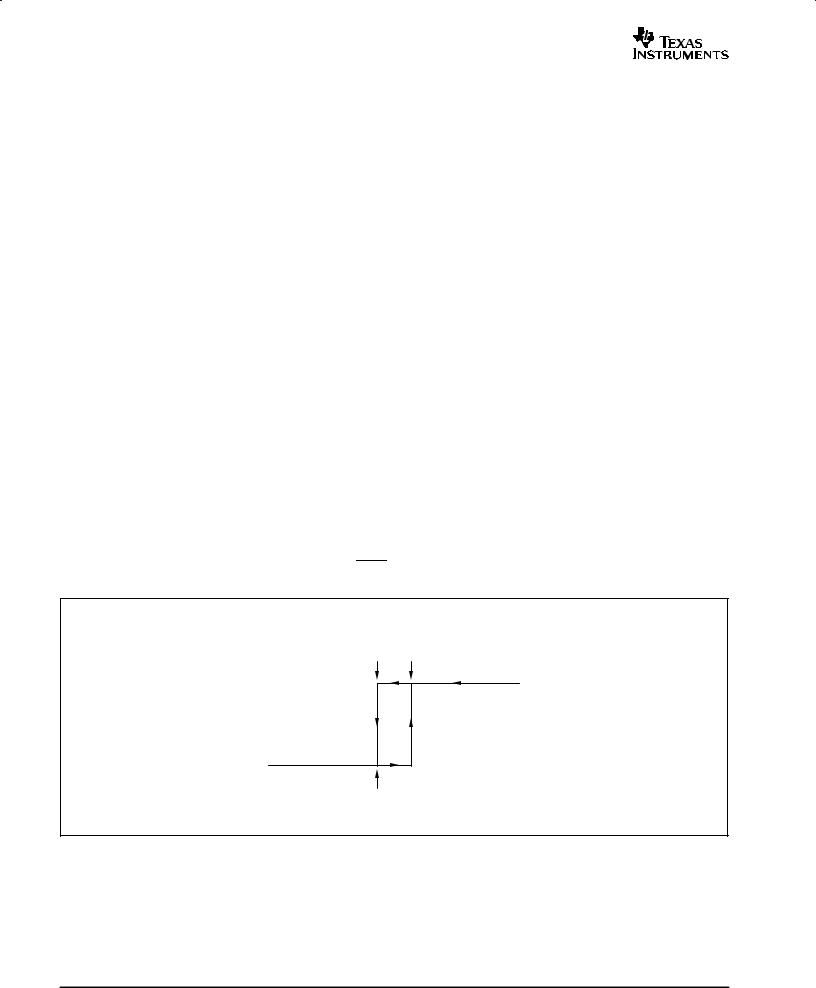
(1)Hysteresis refers to the threshold (the threshold specification applies to a rising edge of a noninverting input) of a falling edge on the noninverting input of the comparator; refer to Figure 1.
(2)Specified by design.
(3)VID refers to the differential voltage at the comparator inputs.
(4)Open-drain output can be pulled to the range of +2.7V to +18V, regardless of VS.
(5)The comparator response time specified is the interval between the input step function and the instant when the output crosses 1.4V.
(6)The RESET input has an internal 2MΩ (typical) pull-down. Leaving RESET open results in a LOW state, with transparent comparator operation.
VTHRESHOLD
0.592V 0.6V
Input Voltage 
Hysteresis = VTHRESHOLD − 8mV
Figure 1. Typical Comparator Hysteresis
4

|
INA200 |
|
INA201 |
www.ti.com |
INA202 |
SBOS374B − NOVEMBER 2006 − REVISED OCTOBER 2007
ELECTRICAL CHARACTERISTICS: GENERAL
Boldface limits apply over the specified temperature range: TA = −40 °C to +125°C.
At TA = +25°C, VS = +12V, VCM = +12V, VSENSE = 100mV, RL = 10kΩ to GND, RPULL-UP = 5.1kΩ connected from CMPOUT to VS, and CMPIN = 1V, unless otherwise noted.
|
|
|
INA200, INA201, INA202 |
|
||
|
|
|
|
|
|
|
GENERAL PARAMETERS |
|
CONDITIONS |
MIN |
TYP |
MAX |
UNITS |
POWER SUPPLY |
|
|
|
|
|
|
Operating Power Supply |
VS |
|
|
|
|
V |
|
+2.7 |
|
+18 |
|||
Quiescent Current |
IQ |
VOUT = 2V |
|
1350 |
1800 |
A |
|
||||||
Over Temperature |
|
VSENSE = 0mV |
|
|
1850 |
A |
Comparator Power-On Reset Threshold(1) |
|
|
|
1.5 |
|
V |
TEMPERATURE |
|
|
|
|
|
|
Specified Temperature Range |
|
|
−40 |
|
+125 |
°C |
Operating Temperature Range |
|
|
−55 |
|
+150 |
°C |
Storage Temperature Range |
|
|
−65 |
|
+150 |
°C |
Thermal Resistance |
qJA |
|
|
|
|
°C/W |
MSOP-8 Surface-Mount |
|
|
|
200 |
|
|
SO-8 |
|
|
|
150 |
|
°C/W |
(1)The INA200, INA201, and INA202 are designed to power-up with the comparator in a defined reset state as long as RESET is open or grounded. The comparator is in reset as long as the power supply is below the voltage shown here. The comparator assumes a state based on the comparator input above this supply voltage. If RESET is high at power-up, the comparator output comes up high and requires a reset to assume a low state, if appropriate.
5

INA200
INA201
INA202 |
www.ti.com |
SBOS374B − NOVEMBER 2006 − REVISED OCTOBER 2007 |
|
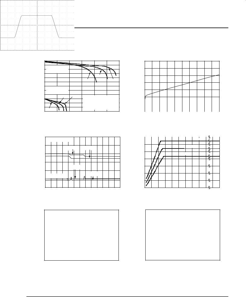
TYPICAL CHARACTERISTICS
At TA = +25°C, VS = +12V, VIN+ = 12V, and VSENSE = 100mV, unless otherwise noted.
GAIN vs FREQUENCY
|
45 |
|
|
CLOAD = 1000pF |
|
40 |
G = 100 |
|
|
|
|
|
|
|
|
35 |
G = 50 |
|
|
|
|
|
|
|
(dB) |
30 |
G = 20 |
|
|
|
|
|
||
25 |
|
|
|
|
Gain |
|
|
|
|
20 |
|
|
|
|
|
|
|
|
|
|
15 |
|
|
|
|
10 |
|
|
|
|
5 |
|
|
|
|
|
10k |
100k |
1M |
|
|
|
Frequency (Hz) |
|
GAIN PLOT
|
20 |
|
|
|
|
|
|
|
|
|
|
|
|
|
|
|
|
|
|
|
|
|
|
|
|
|
|
|
|
|
|
|
|
|
|
|
|
|
|
|
|
|
|
|
|
|
|
|
|
|
|
|
|
|
|
|
18 |
|
|
|
|
|
|
|
|
|
|
|
|
|
|
|
|
|
|
|
|
|
|
|
|
|
|
|
100V/V |
|
|
|
|
|
|
|
|
|
|
|
|
|
|
|
|
|
|
|
|
|
|
|
|||
|
16 |
|
|
|
|
|
|
|
|
|
|
|
|
|
|
|
|
|
|
|
|
|
|
|
|||
|
|
|
|
|
|
|
|
|
|
|
|
|
|
|
|
|
|
|
|
|
|
|
|
|
|
|
|
|
14 |
|
|
|
|
|
|
|
|
|
|
|
|
|
|
|
|
|
|
|
|
|
|
|
|
|
|
|
|
|
|
|
|
|
|
50V/V |
|
|
|
|
|
|
|
|
|
|
|
|
|
|
|
|
|||
|
12 |
|
|
|
|
|
|
|
|
|
|
|
|
|
|
|
|
|
|
|
|
|
|
|
|||
(V) |
|
|
|
|
|
|
|
|
|
|
|
|
|
|
|
|
|
|
|
|
|
|
|
|
|
|
|
|
|
|
|
|
|
|
|
|
|
|
|
|
|
|
|
|
|
|
|
|
|
|
|
|
|
||
10 |
|
|
|
|
|
|
|
|
|
|
|
|
|
|
|
|
|
|
|
|
|
|
|
|
|
|
|
OUT |
|
|
|
|
|
|
|
|
|
|
|
|
|
|
|
|
|
|
|
|
|
|
|
|
|
|
|
|
|
|
|
|
|
|
|
|
|
|
|
|
|
|
|
|
|
|
|
|
|
|
|
|
|
||
|
|
|
|
|
|
|
|
|
|
|
|
|
|
|
|
|
|
|
|
|
|
|
|
|
|
|
|
V |
8 |
|
|
|
|
|
|
|
|
|
|
|
|
|
|
|
|
|
|
|
|
|
|
|
|
|
|
|
|
|
|
|
|
|
|
|
|
|
|
|
20V/V |
|
|
|
|
|
|
|
|
|
|
||||
|
|
|
|
|
|
|
|
|
|
|
|
|
|
|
|
|
|
|
|
|
|
|
|
||||
|
6 |
|
|
|
|
|
|
|
|
|
|
|
|
|
|
|
|
|
|
|
|
|
|
|
|||
|
|
|
|
|
|
|
|
|
|
|
|
|
|
|
|
|
|
|
|
|
|
|
|
|
|
|
|
|
|
|
|
|
|
|
|
|
|
|
|
|
|
|
|
|
|
|
|
|
|
|
|
|
|
|
|
|
4 |
|
|
|
|
|
|
|
|
|
|
|
|
|
|
|
|
|
|
|
|
|
|
|
|
|
|
|
|
|
|
|
|
|
|
|
|
|
|
|
|
|
|
|
|
|
|
|
|
|
|
|
|
|
|
|
2 |
|
|
|
|
|
|
|
|
|
|
|
|
|
|
|
|
|
|
|
|
|
|
|
|
|
|
|
|
|
|
|
|
|
|
|
|
|
|
|
|
|
|
|
|
|
|
|
|
|
|
|
|
|
|
|
0 |
|
|
|
|
|
|
|
|
|
|
|
|
|
|
|
|
|
|
|
|
|
|
|
|
|
|
|
|
100 |
|
|
|
|
|
|
|
|
|
|
|
|
|
|
|
|
|
|
|
|
|
|
|
||
|
20 |
200 |
300 |
400 |
500 |
|
600 |
|
700 |
800 |
900 |
||||||||||||||||
|
|
|
|
|
|
|
|
|
VDIFFERENTIAL (mV) |
|
|
|
|
|
|
|
|
||||||||||
|
4.0 |
|
|
|
|
|
OUTPUT ERROR vs VSENSE |
|
|
|
|
|
|
|
|
||||||||||||
value) |
|
|
|
|
|
|
|
|
|
|
|
|
|
|
|
|
|
|
|
|
|
|
|
|
|
|
|
|
|
|
|
|
|
|
|
|
|
|
|
|
|
|
|
|
|
|
|
|
|
|
|
|
|
||
3.5 |
|
|
|
|
|
|
|
|
|
|
|
|
|
|
|
|
|
|
|
|
|
|
|
|
|
|
|
|
|
|
|
|
|
|
|
|
|
|
|
|
|
|
|
|
|
|
|
|
|
|
|
|
|
|
|
ErrorOutput outputidealtheof |
3.0 |
|
|
|
|
|
|
|
|
|
|
|
|
|
|
|
|
|
|
|
|
|
|
|
|
|
|
|
|
|
|
|
|
|
|
|
|
|
|
|
|
|
|
|
|
|
|
|
|
|
|
|
|
||
2.5 |
|
|
|
|
|
|
|
|
|
|
|
|
|
|
|
|
|
|
|
|
|
|
|
|
|
|
|
|
|
|
|
|
|
|
|
|
|
|
|
|
|
|
|
|
|
|
|
|
|
|
|
|
|
|
|
|
2.0 |
|
|
|
|
|
|
|
|
|
|
|
|
|
|
|
|
|
|
|
|
|
|
|
|
|
|
|
|
|
|
|
|
|
|
|
|
|
|
|
|
|
|
|
|
|
|
|
|
|
|
|
|
|
|
error |
1.5 |
|
|
|
|
|
|
|
|
|
|
|
|
|
|
|
|
|
|
|
|
|
|
|
|
|
|
|
|
|
|
|
|
|
|
|
|
|
|
|
|
|
|
|
|
|
|
|
|
|
|
|
|
||
1.0 |
|
|
|
|
|
|
|
|
|
|
|
|
|
|
|
|
|
|
|
|
|
|
|
|
|
|
|
(% |
|
|
|
|
|
|
|
|
|
|
|
|
|
|
|
|
|
|
|
|
|
|
|
|
|
|
|
0.5 |
|
|
|
|
|
|
|
|
|
|
|
|
|
|
|
|
|
|
|
|
|
|
|
|
|
|
|
|
|
|
|
|
|
|
|
|
|
|
|
|
|
|
|
|
|
|
|
|
|
|
|
|
|
|
|
|
0 |
|
|
|
|
|
|
|
|
|
|
|
|
|
|
|
|
|
|
|
|
|
|
|
|
|
|
|
|
50 |
100 |
|
|
|
|
|
|
|
|
|
|
350 |
400 |
450 |
500 |
||||||||||
|
0 |
150 |
200 |
|
250 |
300 |
|||||||||||||||||||||
VSENSE (mV)
GAIN vs FREQUENCY
|
45 |
|
|
|
40 |
G = 100 |
|
|
|
|
|
|
35 |
G = 50 |
|
|
|
|
|
(dB) |
30 |
G = 20 |
|
|
|
||
25 |
|
|
|
Gain |
|
|
|
20 |
|
|
|
|
|
|
|
|
15 |
|
|
|
10 |
|
|
|
5 |
|
|
|
10k |
100k |
1M |
|
|
Frequency (Hz) |
|
COMMON−MODE AND POWER−SUPPLY REJECTION vs FREQUENCY
|
|
140 |
|
|
|
|
|
|
130 |
|
|
|
|
|
(dB) |
120 |
|
CMR |
|
|
Common−Mode and |
110 |
|
|
|
||
Power−Supply Rejection |
|
|
|
|
||
100 |
|
|
|
|
||
90 |
|
PSR |
|
|
||
80 |
|
|
|
|||
|
|
|
|
|||
70 |
|
|
|
|
||
60 |
|
|
|
|
||
50 |
|
|
|
|
||
|
|
|
|
|
|
|
|
|
40 |
|
|
|
|
|
|
10 |
100 |
1k |
10k |
100k |
|
|
|
|
Frequency (Hz) |
|
|
OUTPUT ERROR vs COMMON−MODE VOLTAGE
|
0.1 |
|
|
|
|
|
|
|
|
|
|
|
0.09 |
|
|
|
|
|
|
|
|
|
|
|
0.08 |
|
|
|
|
|
|
|
|
|
|
) |
0.07 |
|
|
|
|
|
|
|
|
|
|
(% |
|
|
|
|
|
|
|
|
|
|
|
0.06 |
|
|
|
|
|
|
|
|
|
|
|
Error |
|
|
|
|
|
|
|
|
|
|
|
0.05 |
|
|
|
|
|
|
|
|
|
|
|
Output |
0.04 |
|
|
|
|
|
|
|
|
|
|
0.03 |
|
|
|
|
|
|
|
|
|
|
|
|
0.02 |
|
|
|
|
|
|
|
|
|
|
|
0.01 |
|
|
|
|
|
|
|
|
|
|
|
0 |
|
|
|
|
|
|
|
|
|
|
|
− 16 −12 |
− 8 |
−4 |
0 |
4 |
8 |
12 16 |
20 |
... |
76 |
80 |
|
|
|
|
Common−Mode Voltage (V) |
|
|
|
||||
6
|
INA200 |
|
INA201 |
www.ti.com |
INA202 |
SBOS374B − NOVEMBER 2006 − REVISED OCTOBER 2007
TYPICAL CHARACTERISTICS (continued)
At TA = +25°C, VS = +12V, VIN+ = 12V, and VSENSE = 100mV, unless otherwise noted.
Output Voltage (V)
Q
I (mA)
|
|
POSITIVE OUTPUT VOLTAGE SWING |
|
||||||||
|
|
|
vs OUTPUT CURRENT |
|
|
||||||
12 |
|
|
|
|
|
|
|
|
|
|
|
11 |
VS |
= 12V |
|
|
|
|
|
|
|
|
|
10 |
|
|
|
|
|
|
|
|
|||
Sourcing Current |
|
|
|
|
|
|
|
||||
9 |
|
|
|
|
|
|
|
||||
|
|
|
|
|
|
|
+25_C |
|
|
||
8 |
|
|
|
|
|
|
|
|
|
||
|
|
|
|
|
+125_C |
|
− 40_C |
||||
7 |
|
|
|
|
|
|
|||||
|
|
|
|
|
|
|
|
|
|
||
6 |
VS |
= 3V |
|
|
|
|
|
|
|
|
|
5 |
|
|
|
|
|
|
|
|
|||
Sourcing Current |
|
|
|
|
|
|
|
||||
4 |
|
|
|
|
|
|
|
||||
|
|
+25_C |
|
−40_C |
Output |
stage is designed |
|||||
3 |
|
|
|
||||||||
|
|
|
|
|
|
to source current. Current |
|||||
2 |
|
|
|
|
|
|
|||||
|
|
|
|
|
|
sinking |
capability |
is |
|||
1 |
+125 C |
|
|
|
|
approximately 400µA. |
|
||||
0 |
|
_ |
|
|
|
|
|
|
|
|
|
0 |
5 |
10 |
15 |
20 |
25 |
30 |
|||||
|
|||||||||||
|
|
|
Output Current (mA) |
|
|
|
|||||
|
|
|
QUIESCENT CURRENT |
|
|
||||||
|
|
|
vs COMMON−MODE VOLTAGE |
|
|
||||||
2.00 |
VSENSE = 100mV |
|
|
|
|
|
|
|
|||
|
|
|
|
|
|
|
|
||||
1.75 |
|
|
V |
|
= 12V |
|
VS = 2.7V |
|
|
||
|
|
|
|
|
|
|
|||||
|
|
|
S |
|
|
|
|
|
|
||
1.50 |
|
|
|
|
|
|
|
|
|
|
|
1.25 |
|
|
|
|
|
|
|
|
|
|
|
1.00 |
|
|
VS = 12V |
|
|
|
|
||||
|
|
|
|
|
|
VS = 2.7V |
|
|
|||
|
VSENSE = 0mV |
|
|
|
|
|
|||||
0.75 |
|
|
|
|
|
|
|
||||
|
|
|
|
|
|
|
|
|
|
||
0.50 |
|
|
|
|
|
|
|
|
|
|
|
−16 −12 −8 |
−4 0 |
|
4 |
8 |
12 16 |
20 24 |
28 |
32 36 |
|||
|
|
|
|
|
VCM (V) |
|
|
|
|||
|
|
|
|
STEP RESPONSE |
|
|
|
||||
|
|
|
|
|
|
|
|
|
G = 20 |
||
Output Voltage (50mV/div) |
|
|
|
|
|
|
|
|
|
|
|
|
VSENSE = 10mV to 20mV |
|
|
|
|
|
|||||
|
|
|
|
|
Time (2µs/div) |
|
|
|
|||
QUIESCENT CURRENT vs OUTPUT VOLTAGE
|
3.5 |
|
|
3.0 |
|
|
2.5 |
|
(mA) |
2.0 |
|
1.5 |
||
IQ |
||
|
1.0 |
0.5 |
|
|
|
|
|
|
|
|
|
|
|
|
|
|
|
|
|
|
|
|
|
|
|
|
|
0 |
|
|
|
|
|
|
|
|
|
|
|
|
|
|
|
|
|
|
|
|
8 |
9 |
10 |
||
0 |
1 |
2 |
3 |
4 |
5 |
6 |
7 |
|||||
|
|
|
|
|
Output Voltage (V) |
|
|
|
|
|
||
|
|
|
OUTPUT SHORT−CIRCUIT CURRENT |
|
|
|
||||||
|
|
|
|
|
vs SUPPLY VOLTAGE |
|
|
|
|
|||
34 |
|
|
|
|
|
|
|
|
|
|
|
|
|
|
|
|
|
|
|
|
|
|
|
|
|
|
|
|
|
|
|
|
− 40_C |
|
|
|
|
|
|
|
|
|
|
|
|
|
|
|
|
|
|
(mA) |
30 |
|
|
|
|
|
|
+25_C |
|
|
|
|
|
|
|
|
|
|
|
|
|
|
|
||
|
|
|
|
|
|
|
|
|
|
|
|
|
Current |
26 |
|
|
|
|
+125_C |
|
|
|
|
||
|
|
|
|
|
|
|
|
|
||||
22 |
|
|
|
|
|
|
|
|
|
|
|
|
Short−Circuit |
|
|
|
|
|
|
|
|
|
|
|
|
18 |
|
|
|
|
|
|
|
|
|
|
|
|
14 |
|
|
|
|
|
|
|
|
|
|
|
|
|
|
|
|
|
|
|
|
|
|
|
|
|
Output |
10 |
|
|
|
|
|
|
|
|
|
|
|
|
|
|
|
|
|
|
|
|
|
|
|
|
|
6 |
|
|
|
|
|
|
|
|
|
|
|
|
2.5 |
3.5 |
4.5 |
5.5 |
6.5 |
7.5 |
8.5 |
9.5 |
10.5 |
11.5 |
17 |
18 |
|
|
|
|
|
Supply Voltage (V) |
|
|
|
|
|||
STEP RESPONSE
G = 20
Output Voltage (500mV/div)
VSENSE = 10mV to 100mV
Time (2µs/div)
7
 Loading...