


INA270
INA270
INA271
FEATURES DESCRIPTION
APPLICATIONS
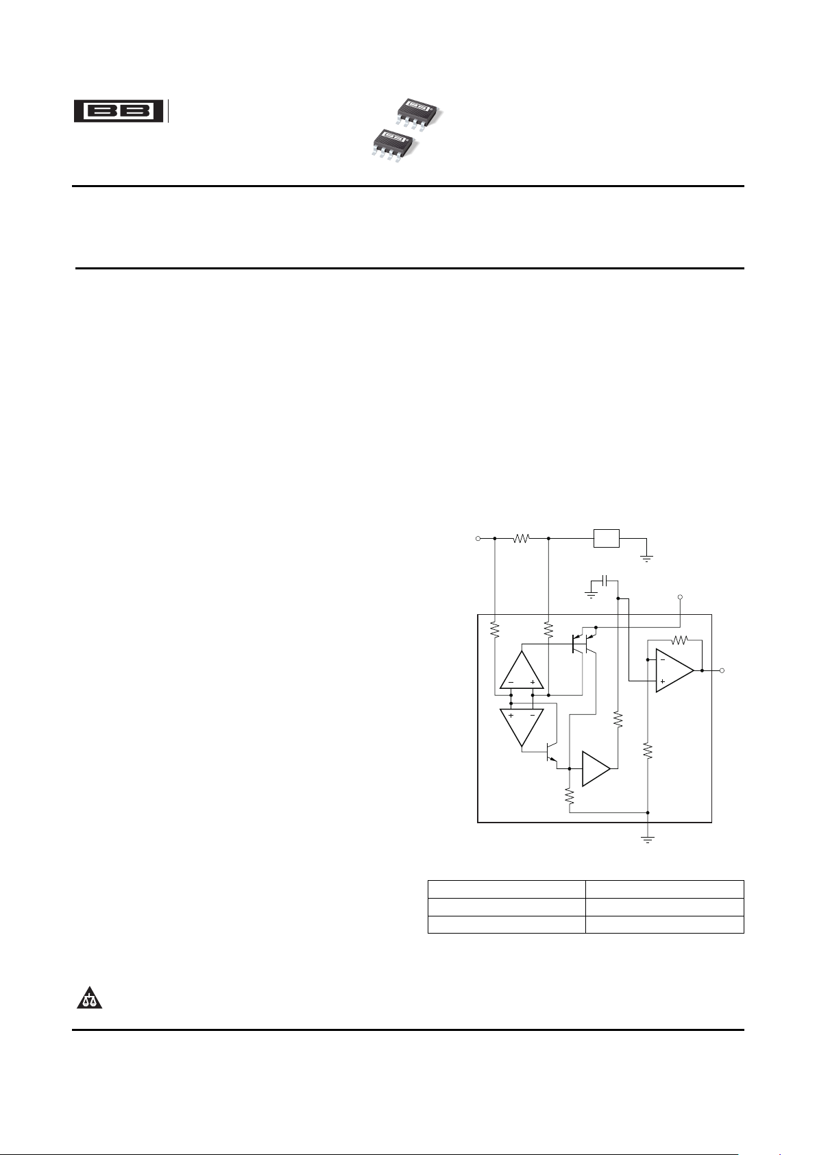
A1
A2
Single-PoleFilter
Capacitor
+2.7Vto+18V
5kW5kW
96kW
R
L
PREOUT BUFIN
GND
OUT
IN-IN+ V+
Load
-16Vto+80V
Supply
R
S
INA270
INA270
INA271
SBOS381A – FEBRUARY 2007 – REVISED APRIL 2007
Voltage Output, Unidirectional Measurement
Current-Shunt Monitor
• WIDE COMMON-MODE RANGE: –16V to +80V
The INA270 and INA271 family of current-shunt
monitors with voltage output can sense drops across
• CMRR: 120dB
current shunts at common-mode voltages from –16V
• ACCURACY:
to +80V, independent of the supply voltage. The
± 2.5mV offset (max)
INA270 and INA271 pinouts readily enable filtering.
± 1% gain error (max)
The INA270 and INA271 are available with two
20 µ V/ ° C offset drift (max)
output voltage scales: 14V/V and 20V/V. The 130kHz
55ppm/ ° C gain drift (max)
bandwidth simplifies use in current-control loops.
• BANDWIDTH: Up to 130kHz
The INA270 and INA271 operate from a single +2.7V
• TWO TRANSFER FUNCTIONS AVAILABLE:
to +18V supply, drawing a maximum of 900 µ A of
14V/V (INA270)
supply current. They are specified over the extended
20V/V (INA271)
operating temperature range of –40 ° C to +125 ° C and
• QUIESCENT CURRENT: 900 µ A (max)
are offered in an SO-8 package.
• POWER SUPPLY: +2.7V to +18V
• PROVISION FOR FILTERING
• POWER MANAGEMENT
• AUTOMOTIVE
• TELECOM EQUIPMENT
• NOTEBOOK COMPUTERS
• BATTERY CHARGERS
• CELL PHONES
• WELDING EQUIPMENT
DEVICE COMPARISON
DEVICE GAIN
INA270 14V/V
INA271 20V/V
Please be aware that an important notice concerning availability, standard warranty, and use in critical applications of Texas
Instruments semiconductor products and disclaimers thereto appears at the end of this data sheet.
All trademarks are the property of their respective owners.
PRODUCTION DATA information is current as of publication date.
Copyright © 2007, Texas Instruments Incorporated
Products conform to specifications per the terms of the Texas
Instruments standard warranty. Production processing does not
necessarily include testing of all parameters.
www.ti.com
ABSOLUTE MAXIMUM RATINGS
(1)
PIN CONFIGURATION
1
2
3
4
8
7
6
5
IN+
NC
(1)
V+
OUT
IN-
GND
PREOUT
BUFIN
INA27x
INA270
INA271
SBOS381A – FEBRUARY 2007 – REVISED APRIL 2007
This integrated circuit can be damaged by ESD. Texas Instruments recommends that all integrated circuits be handled with
appropriate precautions. Failure to observe proper handling and installation procedures can cause damage.
ESD damage can range from subtle performance degradation to complete device failure. Precision integrated circuits may be
more susceptible to damage because very small parametric changes could cause the device not to meet its published
specifications.
ORDERING INFORMATION
(1)
PACKAGE PACKAGE
PRODUCT PACKAGE-LEAD DESIGNATOR GAIN MARKING
INA270 SO-8 D 14 I270A
INA271 SO-8 D 20 I271A
(1) For the most current package and ordering information see the Package Option Addendum at the end of this document, or see the TI
web site at www.ti.com .
INA270, INA271 UNIT
Supply Voltage (V
S
) +18 V
Analog Inputs, V
IN+
, V
IN–
:
Differential, (V
IN+
) – (V
IN–
) –18 to +18 V
Common-Mode –16 to +80 V
Analog Output:
OUT and PRE OUT Pins GND – 0.3 to (V+) + 0.3 V
Input Current Into Any Pin 5 mA
Operating Temperature –55 to +150 ° C
Storage Temperature –65 to +150 ° C
Junction Temperature +150 ° C
ESD Ratings:
Human Body Model 3000 V
Charged-Device Model 750 V
(1) Stresses above these ratings may cause permanent damage. Exposure to absolute maximum conditions for extended periods may
degrade device reliability. These are stress ratings only, and functional operation of the device at these or any other conditions beyond
those specified is not supported.
SO-8
Top View
NOTE (1): NC denotes no internal connection.
2
Submit Documentation Feedback
www.ti.com
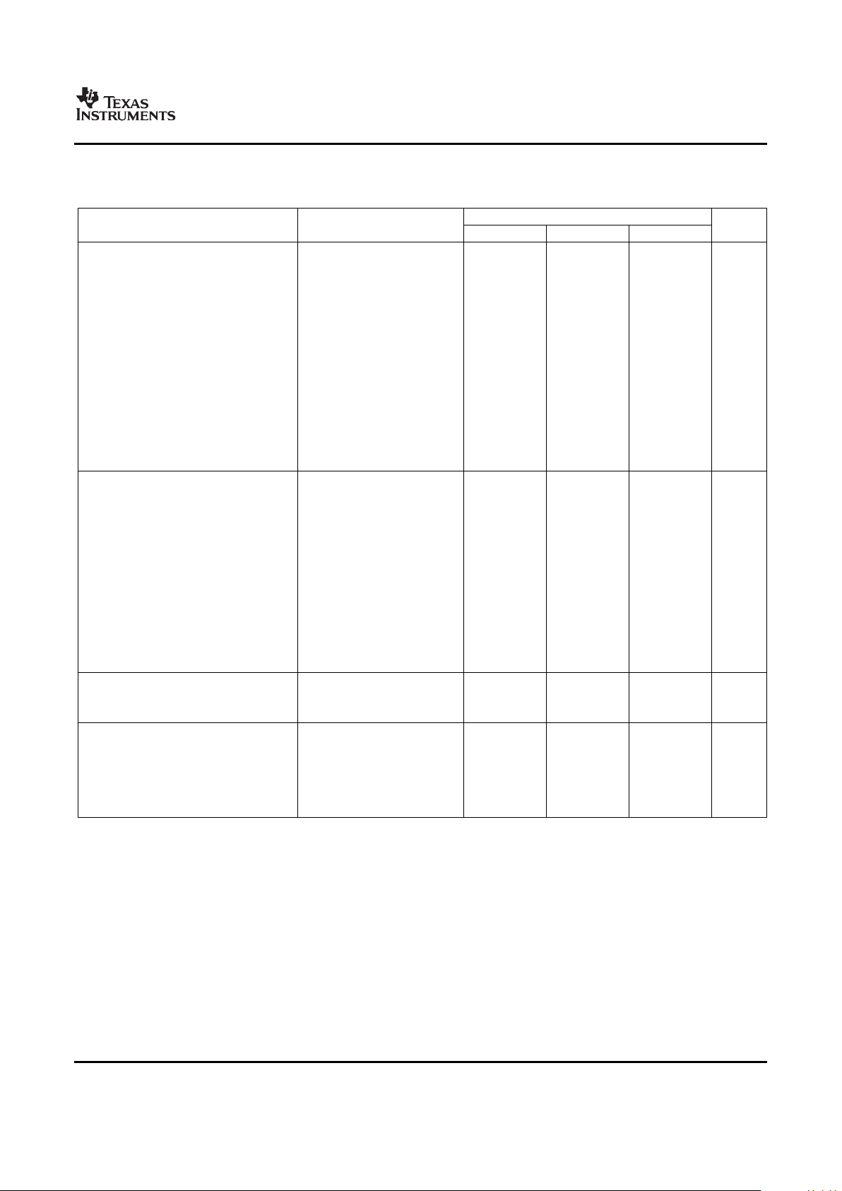
ELECTRICAL CHARACTERISTICS
INA270
INA271
SBOS381A – FEBRUARY 2007 – REVISED APRIL 2007
Boldface limits apply over the specified temperature range: T
A
= –40 ° C to +125 ° C.
At T
A
= +25 ° C, V
S
= +5V, V
CM
= +12V, V
SENSE
= 100mV, and PRE OUT connected to BUF IN, unless otherwise noted.
INA270, INA271
PARAMETER CONDITIONS MIN TYP MAX UNIT
INPUT
Full-Scale Input Voltage V
SENSE
V
SENSE
= (V
IN+
) + (V
IN–
) 0.15 (V
S
– 0.2)/Gain V
Common-Mode Input Range V
CM
–16 +80 V
Common-Mode Rejection Ratio CMRR V
IN+
= –16V to +80V 80 120 dB
Over Temperature V
IN+
= +12V to +80V 100 120 dB
Offset Voltage, RTI
(1)
V
OS
± 0.5 2.5 mV
Over Temperature ± 3 mV
vs Temperature dV
OS
/dT 2.5 20 µ V/ ° C
vs Power-Supply PSR V
S
= +2.7V to +18V, V
CM
= +18V 5 100 µ V/V
Input Bias Current, V
IN–
Pin I
B
± 8 ± 16 µ A
PRE OUT Output Impedance
(2)
96 k Ω
Buffer Input Bias Current –50 nA
Buffer Input Bias Current Temperature
± 0.03 nA/ ° C
Coefficient
OUTPUT (V
SENSE
≥ 20mV)
(3)
Gain: INA270 Total Gain G 14 V/V
Gain: INA271 Total Gain G 20 V/V
Output Buffer Gain G
BUF
2 V/V
Total Gain Error V
SENSE
= 20mV to 100mV ± 0.2 ± 1 %
Over Temperature ± 2 %
vs Temperature 50 ppm/ ° C
Total Output Error
(4)
V
SENSE
= 20mV to 100mV ± 0.75 ± 2.2 %
Total Output Error ± 1.0 ± 3.0 %
Nonlinearity Error V
SENSE
= 20mV to 100mV ± 0.002 %
Output Impedance, Pin 5 R
O
1.5 Ω
Maximum Capacitive Load No Sustained Oscillation 10 nF
VOLTAGE OUTPUT
(5)
R
L
= 10k Ω to GND
Swing to V+ Power-Supply Rail (V+) – 0.05 (V+) – 0.2 V
Swing to GND
(6)
V
GND
+ 0.003 V
GND
+ 0.05 V
FREQUENCY RESPONSE
Bandwidth BW C
LOAD
= 5pF 130 kHz
Phase Margin C
LOAD
< 10nF 40 degrees
Slew Rate SR 1 V/ µ s
Settling Time (1%) t
S
V
SENSE
= 10mV to 100mV
PP
, 2 µ s
C
LOAD
= 5pF
(1) RTI means Referred-to-Input.
(2) Initial resistor variation is ± 30% with an additional –2200ppm/ ° C temperature coefficient.
(3) For output behavior when V
SENSE
< 20mV, see the Application Information section Accuracy Variations as A Result of V
SENSE
and
Common-Mode Voltage.
(4) Total output error includes effects of gain error and V
OS
.
(5) See typical characteristic curve Output Swing vs Output Current and Application Information section Accuracy Variations as A Result of
V
SENSE
and Common-Mode Voltage.
(6) Ensured by design; not production tested.
3
Submit Documentation Feedback
www.ti.com
INA270
INA271
SBOS381A – FEBRUARY 2007 – REVISED APRIL 2007
ELECTRICAL CHARACTERISTICS (continued)
Boldface limits apply over the specified temperature range: T
A
= –40 ° C to +125 ° C.
At T
A
= +25 ° C, V
S
= +5V, V
CM
= +12V, V
SENSE
= 100mV, and PRE OUT connected to BUF IN, unless otherwise noted.
INA270, INA271
PARAMETER CONDITIONS MIN TYP MAX UNIT
NOISE, RTI
(7)
Voltage Noise Density e
n
40 nV/ √ Hz
POWER SUPPLY
Operating Range V
S
+2.7 +18 V
Quiescent Current I
Q
V
OUT
= 2V 700 900 µ A
Over Temperature V
SENSE
= 0mV 350 950 µ A
TEMPERATURE RANGE
Specified Temperature Range –40 +125 ° C
Operating Temperature Range –55 +150 ° C
Thermal Resistance θ
JA
SO-8 +150 ° C/W
(7) RTI means Referred-to-Input.
4
Submit Documentation Feedback
www.ti.com
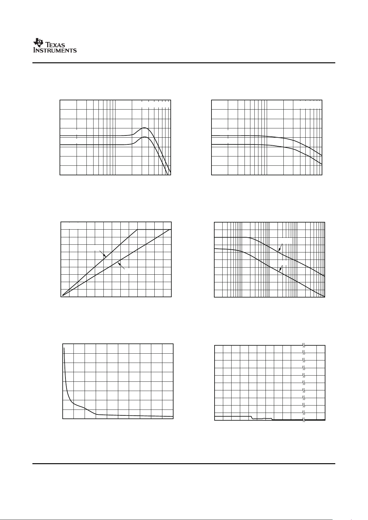
TYPICAL CHARACTERISTICS
45
40
35
30
25
20
15
10
5
10k
100k
Gain(dB)
Frequency(Hz)
1M
C =1000pF
LOAD
G=14
G=20
45
40
35
30
25
20
15
10
5
10k
100k
Gain(dB)
Frequency(Hz)
1M
G=20
G=14
C =0pF
LOAD
140
130
120
110
100
90
80
70
60
50
40
10
100 1k 10k
Common-Modeand
P
ower
-SupplyRejection(dB)
Frequency(Hz)
100k
CMRR
PSR
20
18
16
14
12
10
8
6
4
2
0
0
100
200
300
400
500
600
700
V (V)
OUT
V (mV)
SENSE
800
900
1000
1100
1200
1300
20V/V
14V/V
V =18V
S
4.0
3.5
3.0
2.5
2.0
1.5
1.0
0.5
0
0
50
100
150 200
250 300
350
TotalOutputError
(%erroroftheidealoutputvalue)
V (mV)
SENSE
400 450
500
0.10
0.09
0.08
0.07
0.06
0.05
0.04
0.03
0.02
0.01
0
-16
-12
-8
-4 0
4 128
2016
OutputError(%)
Common-ModeVoltage(V)
... 76
80
INA270
INA271
SBOS381A – FEBRUARY 2007 – REVISED APRIL 2007
At T
A
= +25 ° C, V
S
= +12V, V
CM
= 12V, and V
SENSE
= 100mV, unless otherwise noted.
GAIN vs FREQUENCY GAIN vs FREQUENCY
Figure 1. Figure 2.
COMMON-MODE AND POWER-SUPPLY REJECTION
GAIN PLOT vs FREQUENCY
Figure 3. Figure 4.
TOTAL OUTPUT ERROR vs V
SENSE
OUTPUT ERROR vs COMMON-MODE VOLTAGE
Figure 5. Figure 6.
5
Submit Documentation Feedback
 Loading...