Texas Instruments JM38510-00803BDA, JM38510-00803BCA, SN5407J, SN5417J, SN7407J Datasheet
...
SN5407, SN5417, SN7407, SN7417
HEX BUFFERS/DRIVERS
WITH OPEN-COLLECTOR HIGH-VOLTAGE OUTPUTS
SDLS032A ± DECEMBER 1983 ± REVISED NOVEMBER 1997
D Converts TTL Voltage Levels to MOS |
SN5407, SN5417 . . . J OR W PACKAGE |
|||||
Levels |
SN7407, SN7417 . . . N PACKAGE |
|||||
D High Sink-Current Capability |
|
(TOP VIEW) |
|
|||
|
|
|
|
|
|
|
D Input Clamping Diodes Simplify System |
1A |
|
1 |
14 |
|
VCC |
|
|
|||||
|
|
|||||
Design |
1Y |
|
2 |
13 |
|
6A |
D Open-Collector Driver for Indicator Lamps |
2A |
|
3 |
12 |
|
6Y |
|
|
|||||
|
|
|||||
and Relays |
2Y |
|
4 |
11 |
|
5A |
|
|
|||||
D Inputs Fully Compatible With Most TTL |
3A |
|
5 |
10 |
|
5Y |
3Y |
|
6 |
9 |
|
4A |
|
Circuits |
|
|
||||
|
|
|||||
D Package Options Include Ceramic Flat (W) |
GND |
|
7 |
8 |
|
4Y |
|
|
|
|
|
|
|
Package and Plastic (N) and Ceramic (J) |
|
|
|
|
|
|
DIPs |
|
|
|
|
|
|
description
These monolithic TTL hex buffers/drivers feature high-voltage open-collector outputs for interfacing with high-level circuits (such as MOS), or for driving high-current loads (such as lamps or relays), and also are characterized for use as buffers for driving TTL inputs. The SN5407 and SN7407 have minimum breakdown voltages of 30 V, and the SN5417 and SN7417 have minimum breakdown voltages of 15 V. The maximum sink current is 30 mA for the SN5407 and SN5417 and 40 mA for the SN7407 and SN7417.
These circuits are completely compatible with most TTL families. Inputs are diode clamped to minimize transmission-line effects, which simplifies design. Typical power dissipation is 145 mW and average propagation delay time is 14 ns.
The SN5407 and SN5417 are characterized for operation over the full military temperature range of ±55°C to 125°C. The SN7407 and SN7417 are characterized for operation from 0°C to 70°C.
logic symbol²
1 |
|
2 |
|
|
|
||||
1A |
|
|
|
1Y |
|
4 |
|||
3 |
|
2Y |
||
|
||||
2A |
|
|
|
|
|
|
6 |
||
|
||||
5 |
|
3Y |
||
|
||||
3A |
|
|
|
|
9 |
|
8 |
4Y |
|
|
||||
4A |
|
|
|
|
|
|
10 |
||
|
||||
11 |
|
5Y |
||
|
||||
5A |
|
|
|
|
|
|
12 |
||
|
||||
13 |
|
6Y |
||
|
||||
6A |
|
|
|
|
|
|
|
||
|
||||
² This symbol is in accordance with ANSI/IEEE Std 91-1984 and IEC Publication 617-12.
logic diagram, each buffer/driver (positive logic)
A Y
Y = A
Please be aware that an important notice concerning availability, standard warranty, and use in critical applications of
Texas Instruments semiconductor products and disclaimers thereto appears at the end of this data sheet.
PRODUCTION DATA information is current as of publication date. Products conform to specifications per the terms of Texas Instruments standard warranty. Production processing does not necessarily include testing of all parameters.
Copyright 1997, Texas Instruments Incorporated
POST OFFICE BOX 655303 •DALLAS, TEXAS 75265 |
1 |

SN5407, SN5417, SN7407, SN7417
HEX BUFFERS/DRIVERS
WITH OPEN-COLLECTOR HIGH-VOLTAGE OUTPUTS
SDLS032A ± DECEMBER 1983 ± REVISED NOVEMBER 1997
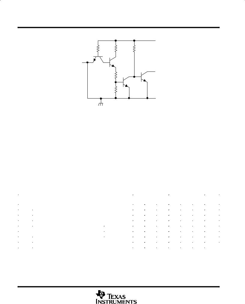
schematic
VCC
6 kΩ |
3.4 kΩ |
1.6 kΩ |
Input A
Output Y
100 Ω
1 kΩ
GND
Resistor values shown are nominal.
absolute maximum ratings over operating free-air temperature range (unless otherwise noted)²
Supply voltage, VCC . . . . . . . . . . . . . . . . . . . . . . . . . . . . . . . . . . . . . . . . . . . . . . . . . . . . . . . . . . . . . . |
. . . . . . . . . . 7 |
V |
Input voltage, VI (see Note 1) . . . . . . . . . . . . . . . . . . . . . . . . . . . . . . . . . . . . . . . . . . . . . . . . . . . . . . . |
. . . . . . . . 5.5 |
V |
Output voltage, VO (see Notes 1 and 2): SN5407, SN7407 . . . . . . . . . . . . . . . . . . . . . . . . . . . . . |
. . . . . . . . . 30 |
V |
SN5417, SN7417 . . . . . . . . . . . . . . . . . . . . . . . . . . . . . |
. . . . . . . . . 15 V |
|
Operating free-air temperature range, TA: SN5407, SN5417 . . . . . . . . . . . . . . . . . . . . . . . . . . |
±55°C to 125°C |
|
SN7407, SN7417 . . . . . . . . . . . . . . . . . . . . . . . . . . . |
. . 0°C to 70°C |
|
Storage temperature range, Tstg . . . . . . . . . . . . . . . . . . . . . . . . . . . . . . . . . . . . . . . . . . . . . . . . . . . |
±65°C to 150°C |
|
²Stresses beyond those listed under ªabsolute maximum ratingsº may cause permanent damage to the device. These are stress ratings only, and functional operation of the device at these or any other conditions beyond those indicated under ªrecommended operating conditionsº is not
implied. Exposure to absolute-maximum-rated conditions for extended periods may affect device reliability.
NOTES: 1. All voltage values are with respect to GND.
2. This is the maximum voltage that should be applied to any output when it is in the off state.
recommended operating conditions
|
|
|
|
SN5407 |
|
|
SN7407 |
|
|
|
|
|
|
SN5417 |
|
|
SN7417 |
|
UNIT |
|
|
|
|
|
|
|
|
|
|
|
|
|
MIN |
NOM |
MAX |
MIN |
NOM |
MAX |
|
|
|
|
|
|
|
|
|
|
|
VCC |
Supply voltage |
|
4.5 |
5 |
5.5 |
4.75 |
5 |
5.25 |
V |
VIH |
High-level input voltage |
|
2 |
|
|
2 |
|
|
V |
VIL |
Low-level input voltage |
|
|
|
0.8 |
|
|
0.8 |
V |
VOH |
High-level output voltage |
SN5407, SN7407 |
|
|
30 |
|
|
30 |
V |
|
|
|
|
|
|
|
|||
SN5417, SN7417 |
|
|
15 |
|
|
15 |
|||
|
|
|
|
|
|
|
|||
|
|
|
|
|
|
|
|
|
|
IOL |
Low-level output current |
|
|
|
30 |
|
|
40 |
mA |
TA |
Operating free-air temperature |
|
±55 |
|
125 |
0 |
|
70 |
°C |
2 |
POST OFFICE BOX 655303 •DALLAS, TEXAS 75265 |
 Loading...