


Texas Instruments TPS2045P, TPS2045DR, TPS2045D, TPS2055P, TPS2055DR Datasheet
...TPS2045, TPS2055 CURRENT-LIMITED POWER-DISTRIBUTION SWITCHES
SLVS182 ± APRIL 1999
features
D135-mΩ -Maximum (5-V Input) High-Side
MOSFET Switch
D250 mA Continuous Current
DShort-Circuit and Thermal Protection With Overcurrent Logic Output
DOperating Range . . . 2.7-V to 5.5-V
DLogic-Level Enable Input
D2.5-ms Typical Rise Time
DUndervoltage Lockout
D10 µA Maximum Standby Supply Current
DBidirectional Switch
DAvailable in 8-pin SOIC and PDIP Packages
DAmbient Temperature Range, ±40°C to 85°C
D2-kV Human-Body-Model, 200-V Machine-Model ESD Protection
typical applications
DNotebook, Desktop and Palmtop PCs
DMonitors, Keyboards, Scanners, and Printers
DDigital Cameras, Phones, and PBXs
DHot-Insertion Applications
|
|
|
|
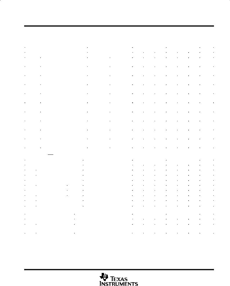
TPS2045 |
|
|
|
|
TPS2055 |
|
|
|
|||||
|
D OR P PACKAGE |
D OR P PACKAGE |
|||||||||||||||
|
|
|
|
(TOP VIEW) |
|
|
|
|
(TOP VIEW) |
|
|
|
|||||
GND |
|
|
|
|
|
OUT |
GND |
|
|
|
|
OUT |
|||||
|
1 |
8 |
|
|
|
1 |
8 |
|
|||||||||
|
|
|
|
|
|||||||||||||
|
IN |
|
2 |
7 |
|
|
OUT |
IN |
|
2 |
7 |
|
OUT |
||||
|
|
|
|
|
|
||||||||||||
|
IN |
|
3 |
6 |
|
|
OUT |
IN |
|
3 |
6 |
|
OUT |
||||
|
|
|
|
|
|
||||||||||||
|
|
|
|
|
|
|
|
|
|
EN |
|
|
|
|
|
|
|
|
EN |
|
|
4 |
5 |
|
|
OC |
|
|
4 |
5 |
|
|
OC |
|
|
|
|
|
|
|
|
|
|
|
|
|
|
|
|
|
|
|
|
|
|
|
|
|
|
|
|
|
|
|
|
|
|
|
|
|
|
description
The TPS2045 and TPS2055 power-distribution switches are intended for applications where heavy capacitive loads and short circuits are likely. Each of these 135-mΩ N-channel MOSFET high-side power switches is controlled by a logic enable compatible with 5-V and 3-V logic. Gate drive is provided by an internal charge pump that controls the power-switch rise times and fall times to minimize current surges during switching. The charge pump requires no external components and allows operation from supplies as low as 2.7 V.
When the output load exceeds the current-limit threshold or a short is present, the TPS2045 and TPS2055 limit the output current to a safe level by switching into a constant-current mode, pulling the overcurrent (OC) logic output low. When continuous heavy overloads and short circuits increase the power dissipation in the switch, causing the junction temperature to rise, a thermal protection circuit shuts off the switch in overcurrent to prevent damage. Recovery from a thermal shutdown is automatic once the device has cooled sufficiently. Internal circuitry ensures the switch remains off until valid input voltage is present.
The TPS2045 and TPS2055 are designed to limit at 0.44-A load. These power-distribution switches, available in 8-pin small-outline integrated circuit (SOIC) and 8-pin plastic dual-in-line packages (PDIP), operate over an ambient temperature range of ±40°C to 85°C.
AVAILABLE OPTIONS
|
|
RECOMMENDED |
TYPICAL SHORT-CIRCUIT |
PACKAGED DEVICES |
||
|
|
MAXIMUM CONTINUOUS |
|
|
||
TA |
ENABLE |
CURRENT LIMIT AT 25°C |
SOIC |
PDIP |
||
LOAD CURRENT |
||||||
|
|
(A) |
(A) |
(D)² |
(P) |
|
|
|
|
||||
±40°C to 85°C |
Active low |
0.25 |
0.44 |
TPS2045D |
TPS2045P |
|
|
|
|
|
|
|
|
±40°C to 85°C |
Active high |
0.25 |
0.44 |
TPS2055D |
TPS2055P |
|
² The D package is available taped and reeled. Add an R suffix to device type (e.g., TPS2045DR)
Please be aware that an important notice concerning availability, standard warranty, and use in critical applications of Texas Instruments semiconductor products and disclaimers thereto appears at the end of this data sheet.
This document contains information on products in more than one phase |
Copyright 1999, Texas Instruments Incorporated |
of development. The status of each device is indicated on the page(s) |
|
specifying its electrical characteristics. |
|
POST OFFICE BOX 655303 •DALLAS, TEXAS 75265 |
1 |

TPS2045, TPS2055
CURRENT-LIMITED POWER-DISTRIBUTION SWITCHES
SLVS182 ± APRIL 1999
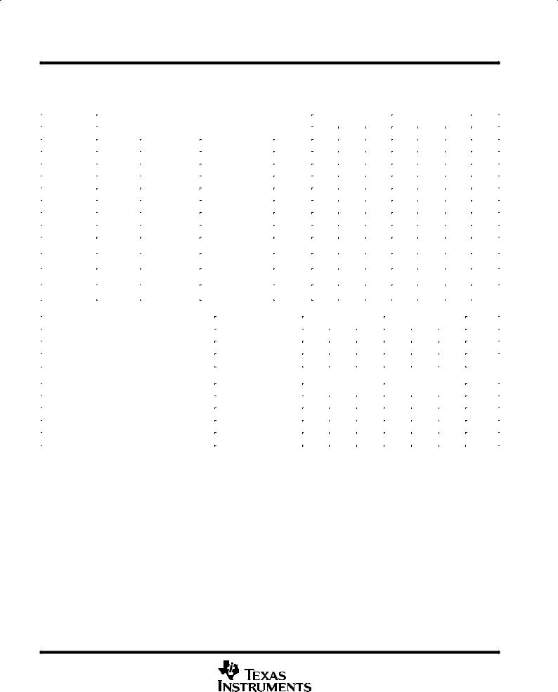
TPS2045 functional block diagram
|
Power Switch |
|
|
|
|
² |
|
IN |
|
CS |
OUT |
|
Charge |
|
|
|
Pump |
|
|
EN |
Driver |
Current |
|
Limit |
|
||
|
|
|
|
|
|
|
OC |
|
UVLO |
|
|
|
Thermal |
|
|
GND |
Sense |
|
|
² Current Sense
|
|
|
|
|
|
|
|
Terminal Functions |
|
|
|
|
|
|
|
|
|
|
|
|
|
TERMINAL |
|
|
|
|
|
|
|
|
|
|
|
|
|
|
|
|
|
NO. |
|
I/O |
DESCRIPTION |
|
|
NAME |
|
|
|
||||
|
D OR P |
|||||||
|
|
|
||||||
|
|
|
|
|
|
|
|
|
|
|
|
|
TPS2045 |
|
TPS2055 |
|
|
|
|
|
|
|
|
|
|
|
|
|
|
|
4 |
|
± |
I |
Enable input. Logic low turns on power switch. |
|
EN |
|
|
|
||||
|
|
|
|
|
|
|
|
|
|
EN |
± |
|
4 |
I |
Enable input. Logic high turns on power switch. |
||
|
|
|
|
|
|
|
|
|
|
GND |
1 |
|
1 |
I |
Ground |
||
|
|
|
|
|
|
|
|
|
|
IN |
2, 3 |
|
2, 3 |
I |
Input voltage |
||
|
|
|
|
|
|
|
||
|
|
|
|
5 |
|
5 |
O |
Over current. Logic output active low |
|
OC |
|
|
|||||
|
|
|
|
|
|
|
||
|
OUT |
6, 7, 8 |
|
6, 7, 8 |
O |
Power-switch output |
||
2 |
POST OFFICE BOX 655303 •DALLAS, TEXAS 75265 |

TPS2045, TPS2055
CURRENT-LIMITED POWER-DISTRIBUTION SWITCHES
SLVS182 ± APRIL 1999
detailed description
power switch
The power switch is an N-channel MOSFET with a maximum on-state resistance of 135 mΩ (VI(IN) = 5 V). Configured as a high-side switch, the power switch prevents current flow from OUT to IN and IN to OUT when
disabled. The power switch can supply a minimum of 250 mA per switch.
charge pump
An internal charge pump supplies power to the driver circuit and provides the necessary voltage to pull the gate of the MOSFET above the source. The charge pump operates from input voltages as low as 2.7 V and requires very little supply current.
driver
The driver controls the gate voltage of the power switch. To limit large current surges and reduce the associated electromagnetic interference (EMI) produced, the driver incorporates circuitry that controls the rise times and fall times of the output voltage. The rise and fall times are typically in the 2-ms to 4-ms range.
enable (EN or EN)
The logic enable disables the power switch and the bias for the charge pump, driver, and other circuitry to reduce the supply current to less than 10 µA when a logic high is present on EN (TPS2045) or a logic low is present on EN (TPS2055). A logic zero input on EN or a logic high on EN restores bias to the drive and control circuits and turns the power on. The enable input is compatible with both TTL and CMOS logic levels.
overcurrent (OC)
The OC open-drain output is asserted (active low) when an overcurrent or overtemperature condition is encountered. The output will remain asserted until the overcurrent or overtemperature condition is removed.
current sense
A sense FET monitors the current supplied to the load. The sense FET measures current more efficiently than conventional resistance methods. When an overload or short circuit is encountered, the current-sense circuitry sends a control signal to the driver. The driver in turn reduces the gate voltage and drives the power FET into its saturation region, which switches the output into a constant current mode and holds the current constant while varying the voltage on the load.
thermal sense
An internal thermal-sense circuit shuts off the power switch when the junction temperature rises to approximately 140°C. Hysteresis is built into the thermal sense circuit. After the device has cooled approximately 20°C, the switch turns back on. The switch continues to cycle off and on until the fault is removed.
undervoltage lockout
A voltage sense circuit monitors the input voltage. When the input voltage is below approximately 2 V, a control signal turns off the power switch.
POST OFFICE BOX 655303 •DALLAS, TEXAS 75265 |
3 |

TPS2045, TPS2055
CURRENT-LIMITED POWER-DISTRIBUTION SWITCHES
SLVS182 ± APRIL 1999
absolute maximum ratings over operating free-air temperature range (unless otherwise noted)²
Input voltage range, VI(IN) (see Note 1) . . . . . . . . . . . . . . . . . . . . . . . . . . . . . . . . . . . . . . . . . . . . . . . . ±0.3 V to 6 V Output voltage range, VO(OUT) (see Note 1) . . . . . . . . . . . . . . . . . . . . . . . . . . . . . . . . . . . ±0.3 V to VI(IN) + 0.3 V Input voltage range, VI(EN) or VI(EN) . . . . . . . . . . . . . . . . . . . . . . . . . . . . . . . . . . . . . . . . . . . . . . . . . . ±0.3 V to 6 V Continuous output current, IO(OUT) . . . . . . . . . . . . . . . . . . . . . . . . . . . . . . . . . . . . . . . . . . . . . . . . . internally limited Continuous total power dissipation . . . . . . . . . . . . . . . . . . . . . . . . . . . . . . . . . . . . . . See Dissipation Rating Table
Operating virtual junction temperature range, TJ . . . . . . . . . . . . . . . . . . . . . . . . . . . . . . . . . . . . . . ±40°C to 125°C Storage temperature range, Tstg . . . . . . . . . . . . . . . . . . . . . . . . . . . . . . . . . . . . . . . . . . . . . . . . . . . . ±65°C to 150°C Lead temperature soldering 1,6 mm (1/16 inch) from case for 10 seconds . . . . . . . . . . . . . . . . . . . . . . . 260°C
Electrostatic discharge (ESD) protection: Human body model MIL-STD-883C . . . . . . . . . . . . . . . . . . . . . 2 kV Machine model . . . . . . . . . . . . . . . . . . . . . . . . . . . . . . . . . . . . . 0.2 kV
²Stresses beyond those listed under ªabsolute maximum ratingsº may cause permanent damage to the device. These are stress ratings only, and functional operation of the device at these or any other conditions beyond those indicated under ªrecommended operating conditionsº is not
implied. Exposure to absolute-maximum-rated conditions for extended periods may affect device reliability. NOTE 1: All voltages are with respect to GND.
|
|
|
|
|
DISSIPATION RATING TABLE |
|
|
|
|
|
||
|
|
|
PACKAGE |
TA ≤ 25°C |
DERATING FACTOR |
TA = 70°C |
TA = 85°C |
|
|
|
||
|
|
|
POWER RATING |
ABOVE TA = 25°C |
POWER RATING POWER RATING |
|
|
|||||
|
|
|
|
|
|
|||||||
|
|
|
D |
725 mW |
5.8 mW/°C |
464 mW |
377 mW |
|
|
|
||
|
|
|
P |
1175 mW |
9.4 mW/°C |
752 mW |
611 mW |
|
|
|
||
recommended operating conditions |
|
|
|
|
|
|
|
|
||||
|
|
|
|
|
|
|
|
|
|
|
||
|
|
|
|
|
|
|
TPS2045 |
|
TPS2055 |
UNIT |
||
|
|
|
|
|
|
|
|
|
|
|
|
|
|
|
|
|
|
|
|
MIN |
MAX |
|
MIN |
MAX |
|
|
|
|
|
|
|
|
|
|
||||
|
|
|
|
|
|
|
|
|
|
|
|
|
Input voltage, VI(IN) |
|
|
|
2.7 |
5.5 |
|
2.7 |
5.5 |
V |
|||
|
|
|
or VI(EN) |
|
|
|
0 |
5.5 |
|
0 |
5.5 |
V |
Input voltage, VI(EN) |
|
|
|
|
||||||||
Continuous output current, IO(OUT) |
|
|
|
0 |
250 |
|
0 |
250 |
mA |
|||
Operating virtual junction temperature, TJ |
|
|
±40 |
125 |
|
±40 |
125 |
°C |
||||
4 |
POST OFFICE BOX 655303 •DALLAS, TEXAS 75265 |
TPS2045, TPS2055
CURRENT-LIMITED POWER-DISTRIBUTION SWITCHES
SLVS182 ± APRIL 1999
electrical characteristics over recommended operating junction temperature range, VI(IN)= 5.5 V, IO = rated current, VI(EN)= 0 V, VI(EN) = Hi (unless otherwise noted)
power switch
|
PARAMETER |
TEST CONDITIONS² |
TPS2045 |
|
TPS2055 |
|
UNIT |
|
|
|
|
|
|
||||
|
MIN TYP |
MAX |
MIN TYP |
MAX |
||||
|
|
|
|
|
||||
|
|
|
|
|
|
|
|
|
|
|
VI(IN) = 5 V, |
TJ = 25°C, |
80 |
95 |
80 |
95 |
|
|
|
IO = 0.25 A |
|
|
||||
|
|
|
|
|
|
|
|
|
|
Static drain-source on-state |
VI(IN) = 5 V, |
TJ = 85°C, |
90 |
120 |
90 |
120 |
|
|
resistance, 5-V operation |
IO = 0.25 A |
|
|
||||
|
|
|
|
|
|
|
||
|
|
VI(IN) = 5 V, |
TJ = 125°C, |
100 |
135 |
100 |
135 |
mΩ |
|
|
IO = 0.25 A |
|
|||||
rDS(on) |
|
|
|
|
|
|
|
|
|
VI(IN) = 3.3 V, |
TJ = 25°C, |
85 |
105 |
85 |
105 |
|
|
|
|
|
||||||
|
|
IO = 0.25 A |
|
|
||||
|
|
|
|
|
|
|
|
|
|
Static drain-source on-state |
VI(IN) = 3.3 V, |
TJ = 85°C, |
100 |
135 |
100 |
135 |
|
|
resistance, 3.3-V operation |
IO = 0.25 A |
|
|
||||
|
|
|
|
|
|
|
||
|
|
VI(IN) = 3.3 V, |
TJ = 125°C, |
115 |
150 |
115 |
150 |
|
|
|
IO = 0.25 A |
|
|
||||
|
|
|
|
|
|
|
|
|
|
|
VI(IN) = 5.5 V, |
TJ = 25°C, |
2.5 |
|
2.5 |
|
|
|
|
CL = 1 µF, |
RL = 20 Ω |
|
|
|
||
tr |
Rise time, output |
|
|
|
|
ms |
||
VI(IN) = 2.7 V, |
TJ = 25°C, |
3 |
|
3 |
|
|||
|
|
|
|
|
||||
|
|
CL = 1 µF, |
RL = 20 Ω |
|
|
|
||
|
|
|
|
|
|
|
||
|
|
VI(IN) = 5.5 V, |
TJ = 25°C, |
4.4 |
|
4.4 |
|
|
|
|
CL = 1 µF, |
RL = 20 Ω |
|
|
|
||
tf |
Fall time, output |
|
|
|
|
ms |
||
VI(IN) = 2.7 V, |
TJ = 25°C, |
2.5 |
|
2.5 |
|
|||
|
|
|
|
|
||||
|
|
CL = 1 µF, |
RL = 20 Ω |
|
|
|
||
|
|
|
|
|
|
|
||
² Pulse-testing techniques maintain junction temperature close to ambient temperature; thermal effects must be taken into account separately.
enable input EN or EN
|
PARAMETER |
|
|
TEST CONDITIONS |
TPS2045 |
|
|
TPS2055 |
UNIT |
||
|
|
|
|
|
|
|
|||||
|
MIN TYP |
MAX |
MIN |
TYP MAX |
|||||||
|
|
|
|
|
|
|
|
||||
|
|
|
|
|
|
|
|
|
|
|
|
VIH |
High-level input voltage |
2.7 V ≤ VI(IN) ≤ 5.5 V |
2 |
|
2 |
|
V |
||||
VIL |
Low-level input voltage |
4.5 V ≤ VI(IN) ≤ 5.5 V |
|
0.8 |
|
0.8 |
V |
||||
2.7 V ≤ VI(IN) ≤ 4.5 V |
|
0.4 |
|
0.4 |
|
||||||
|
|
|
|
|
|
||||||
II |
Input current |
TPS2045 |
VI(EN) |
= 0 V or VI(EN) = VI(IN) |
±0.5 |
0.5 |
|
|
µA |
||
|
|
|
|
|
|
|
|
|
|||
TPS2055 |
VI(EN) = VI(IN) or VI(EN) = 0 V |
|
|
±0.5 |
0.5 |
||||||
|
|
|
|
|
|||||||
ton |
Turnon time |
CL = 100 µF, |
RL = 20 Ω |
|
20 |
|
20 |
ms |
|||
toff |
Turnoff time |
CL = 100 µF, |
RL = 20 Ω |
|
40 |
|
40 |
|
|||
current limit
PARAMETER |
TEST CONDITIONS² |
|
TPS2045 |
|
|
TPS2055 |
|
UNIT |
|
|
|
|
|
|
|
||||
MIN |
TYP |
MAX |
MIN |
TYP |
MAX |
||||
|
|
|
|||||||
|
|
|
|
|
|
|
|
|
|
IOS Short-circuit output current |
VI(IN) = 5 V, OUT connected to GND, |
0.345 |
0.44 |
0.525 |
0.345 |
0.44 |
0.525 |
A |
|
Device enabled into short circuit |
|||||||||
|
|
|
|
|
|
|
|
² Pulse-testing techniques maintain junction temperature close to ambient temperature; thermal effects must be taken into account separately.
POST OFFICE BOX 655303 •DALLAS, TEXAS 75265 |
5 |
TPS2045, TPS2055
CURRENT-LIMITED POWER-DISTRIBUTION SWITCHES
SLVS182 ± APRIL 1999
electrical characteristics over recommended operating junction temperature range, VI(IN)= 5.5 V, IO = rated current, VI(EN) = 0 V, VI(EN) = Hi (unless otherwise noted) (continued)
supply current
PARAMETER |
|
|
|
|
TEST CONDITIONS |
|
|
|
|
TPS2045 |
|
TPS2055 |
|
UNIT |
|||
|
|
|
|
|
|
|
|
|
|
|
|
||||||
|
|
|
|
|
|
|
MIN |
TYP |
MAX |
MIN TYP |
MAX |
||||||
|
|
|
|
|
|
|
|
|
|
|
|
|
|||||
|
|
|
|
|
|
|
|
|
|
|
|
|
|
|
|
||
Supply |
|
|
|
|
|
TJ = 25°C |
|
|
TPS2045 |
|
0.015 |
1 |
|
|
|
||
|
VI(EN) |
= VI(IN) |
|
|
|
|
|
|
|
|
|
|
|
||||
No Load |
° |
≤ |
TJ |
≤ |
° |
|
|
10 |
|
|
|
||||||
current, |
|
|
|
|
|
|
|||||||||||
|
|
|
|
±40 C |
|
|
125 C |
|
|
|
|
|
A |
||||
low-level |
on OUT |
|
|
|
|
|
° |
|
|
|
|
|
|
|
0.015 |
1 |
|
|
|
|
|
|
|
|
|
|
|
|
|
|
|||||
output |
|
VI(EN) |
= 0 V |
TJ = 25 C |
|
|
TPS2055 |
|
|
|
|
||||||
|
±40°C |
≤ TJ |
≤ |
125°C |
|
|
|
|
10 |
|
|||||||
|
|
|
|
|
|
|
|
|
|
|
|
||||||
Supply |
|
|
|
|
|
TJ = 25°C |
|
|
TPS2045 |
|
80 |
100 |
|
|
|
||
|
VI(EN) |
|
= 0 V |
|
|
|
|
|
|
|
|
|
|
|
|||
No Load |
|
±40°C |
≤ TJ |
≤ |
125°C |
|
100 |
|
|
|
|
||||||
current, |
|
|
|
|
|
|
|
|
|
A |
|||||||
high-level |
on OUT |
|
|
|
|
|
° |
|
|
|
|
|
|
|
80 |
100 |
|
|
|
|
|
|
|
|
|
|
|
|
|
|
|||||
output |
|
VI(EN) |
= VI(IN) |
TJ = 25 C |
|
|
TPS2055 |
|
|
|
|
||||||
|
±40°C |
≤ TJ |
≤ |
125°C |
|
|
|
100 |
|
|
|||||||
|
|
|
|
|
|
|
|
|
|
|
|
||||||
|
OUT |
|
|
|
|
±40°C ≤ TJ |
≤ 125°C |
|
|
|
|
|
|
|
|||
Leakage |
VI(EN) |
= VI(IN) |
TPS2045 |
|
100 |
|
|
|
A |
||||||||
current |
connected |
|
|
|
|
|
|
|
|
|
|
|
|
|
|
|
|
VI(EN) = 0 V |
±40°C ≤ TJ |
≤ 125°C |
TPS2055 |
|
|
|
100 |
|
|||||||||
to ground |
|
|
|
|
|
||||||||||||
|
|
|
|
|
|
||||||||||||
Reverse |
|
|
|
|
|
|
|
|
|
|
|
|
|
|
|
|
|
IN = high |
VI(EN) |
= 0 V |
TJ = 25°C |
|
|
TPS2045 |
|
0.3 |
|
|
|
A |
|||||
leakage |
impedance |
|
|
|
|
|
|
|
|
|
|
|
|
||||
VI(EN) = Hi |
|
|
TPS2055 |
|
|
|
0.3 |
|
|||||||||
current |
|
|
|
|
|
|
|
|
|
|
|||||||
|
|
|
|
|
|
|
|
|
|
|
|||||||
undervoltage lockout
|
PARAMETER |
TEST CONDITIONS |
|
TPS2045 |
|
TPS2055 |
UNIT |
||||
|
|
|
|
|
|
|
|||||
MIN |
TYP |
MAX |
MIN |
TYP |
MAX |
||||||
|
|
|
|
|
|||||||
|
|
|
|
|
|
|
|
|
|
|
|
Low-level input voltage |
|
2 |
|
2.5 |
2 |
|
2.5 |
V |
|||
|
|
|
|
|
|
|
|
|
|
|
|
Hysteresis |
TJ = 25°C |
|
100 |
|
|
100 |
|
mV |
|||
|
|
|
|
|
|
|
|
|
|
|
|
overcurrent OC
PARAMETER |
TEST CONDITIONS |
TPS2045 |
|
TPS2055 |
UNIT |
||||
|
|
|
|||||||
MIN TYP |
MAX |
MIN TYP MAX |
|||||||
|
|
|
|
|
|
||||
|
|
|
|
|
|
|
|
|
|
Sink current² |
VO = 5 V |
|
|
|
|
10 |
10 |
mA |
|
Output low voltage |
IO = 5 V, |
|
|
|
|
|
|
|
|
VOL(OC) |
|
|
0.5 |
0.5 |
V |
||||
Off-state current² |
VO = 5 V, |
VO = 3.3 V |
|
1 |
1 |
A |
|||
² Specified by design, not production tested. |
|
|
|
|
|
|
|
|
|
6 |
POST OFFICE BOX 655303 •DALLAS, TEXAS 75265 |

TPS2045, TPS2055
CURRENT-LIMITED POWER-DISTRIBUTION SWITCHES
SLVS182 ± APRIL 1999
PARAMETER MEASUREMENT INFORMATION
|
OUT |
|
|
|
|
|
|
|
|
RL |
CL |
tr |
|
|
tf |
|
|
|
|
|
|
||
|
|
|
|
VO(OUT) |
|
90% |
90% |
|
|
|
|
|
10% |
10% |
|
|
TEST CIRCUIT |
|
|
|
|
|
|
VI(EN) |
50% |
50% |
|
VI(EN) |
50% |
50% |
|
|
ton |
|
toff |
ton |
|
|
toff |
VO(OUT) |
|
90% |
|
VO(OUT) |
|
90% |
|
|
|
|
10% |
|
|
|
10% |
VOLTAGE WAVEFORMS
Figure 1. Test Circuit and Voltage Waveforms
VI(EN)
(5 V/div)
VO(OUT)
(2 V/div)
VI(EN)
(5 V/div)
|
|
|
|
|
|
|
|
VI(IN) = 5 V |
|
|
V |
||
|
|
|
|
|
|
|
|
|
° |
|
|
|
|
|
|
|
|
|
|
|
|
TA = 25 C |
|
|
|
O(OUT) |
|
|
|
|
|
|
|
|
|
CL = 0.1 F |
|
|
(2 V/div) |
||
|
|
|
|
|
|
|
|
|
|
|
|
|
0 |
0 |
1 |
2 |
3 |
4 |
5 |
6 |
7 |
8 |
9 |
10 |
|||
|
|
|
|
|
t ± Time ± ms |
|
|
|
|
|
|
||
VI(IN) = 5 |
V |
|
|
|
|
TA = 25°C |
|
|
|
|
|
CL = 0.1 F |
|
|
|
|
|
|
|
|
|
|
|
1000 |
2000 |
3000 |
4000 |
5000 |
|
|
t ± Time ± ms |
|
|
|
|
Figure 2. Turnon Delay and Rise Time
with 0.1- F Load
Figure 3. Turnoff Delay and Fall Time
with 0.1- F Load
POST OFFICE BOX 655303 •DALLAS, TEXAS 75265 |
7 |
 Loading...