


TPS3836K33DBVT
Texas Instruments TPS3836K33DBVT, TPS3836K33DBVR, TPS3836J25DBVT, TPS3836J25DBVR, TPS3836H30DBVT Datasheet
...
TPS3836E18 / J25 / H30 / L30 / K33
TPS3837E18 / J25 / L30 / K33, TPS3838E18 / J25 / L30 / K33
NANOPOWER SUPERVISORY CIRCUITS
SLVS292A – JUNE 2000 – REVISED JANUARY 2002
D Supply Current of 220 nA (Typ)
D Precision Supply Voltage Supervision
Range: 1.8 V, 2.5 V, 3.0 V, 3.3 V
D Power-On Reset Generator With Selectable
Delay Time of 10 ms or 200 ms
D Push/Pull RESET Output (TPS3836),
RESET Output (TPS3837), or
Open-Drain RESET
Output (TPS3838)
D Manual Reset
D 5-Pin SOT-23 Package
D Temperature Range –40°C to 85°C
D Applications Include
– Applications Using Low-Power DSPs,
Microcontrollers, or Microprocessors
– Portable/Battery-Powered Equipment
– Intelligent Instruments
– Wireless Communication Systems
– Notebook Computers
– Automotive Systems
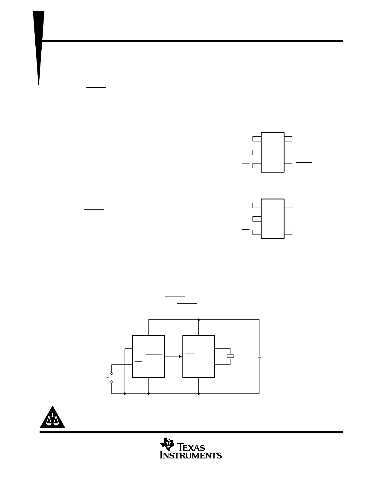
TPS3836, TPS3838
DBV PACKAGE
(TOP VIEW)
CT
1
description
GND
The TPS3836, TPS3837, TPS3838 families of
supervisory circuits provide circuit initialization
MR
and timing supervision, primarily for DSP and
processor-based systems.
During power on, RESET
supply voltage V
DD
Thereafter, the supervisory circuit monitors V
and keeps RESET output active as long as V
remains below the threshold voltage VIT. An
is asserted when the
becomes higher than 1.1 V.
DD
DD
CT
GND
internal timer delays the return of the output to the
inactive state (high) to ensure proper system
reset. The delay time starts after V
above the threshold voltage V
.
IT
has risen
DD
MR
When CT is connected to GND a fixed delay time of typical 10 ms is asserted. When connected to V
time is typically 200 ms.
2
3
TPS3837
DBV PACKAGE
(TOP VIEW)
1
2
3
5
V
DD
4
RESET
V
5
4
DD
RESET
the delay
DD
When the supply voltage drops below the threshold voltage V
All the devices of this family have a fixed-sense threshold voltage V
The TPS3836 has an active-low push-pull RESET
TPS3838 integrates an active-low open-drain RESET
TPS3836K33
V
DD
CT
RESET
MR
T
Please be aware that an important notice concerning availability, standard warranty, and use in critical applications of
Texas Instruments semiconductor products and disclaimers thereto appears at the end of this data sheet.
PRODUCTION DATA information is current as of publication date.
Products conform to specifications per the terms of Texas Instruments
standard warranty. Production processing does not necessarily include
testing of all parameters.
GND
TYPICAL OPERATING CIRCUIT
output. The TPS3837 has active-high push-pull RESET , and
output.
V
CC
RST
Xout
V
SS
MSP430
Xin
, the output becomes active (low) again.
IT
set by an internal voltage divider.
IT
Lithium
Battery
Quartz
32 kHz
3.6 V
Copyright 2002, Texas Instruments Incorporated
POST OFFICE BOX 655303 • DALLAS, TEXAS 75265
1
TPS3836E18 / J25 / H30 / L30 / K33
40 C to 85 C
TPS3837E18 / J25 / L30 / K33, TPS3838E18 / J25 / L30 / K33
NANOPOWER SUPERVISORY CIRCUITS
SLVS292A – JUNE 2000 – REVISED JANUARY 2002
description (continued)
The product spectrum is designed for supply voltages of 1.8 V , 2.5 V, 3 V , and 3.3 V. The circuits are available
in a 5-pin SOT-23 package. The TPS3836, TPS3837, TPS3838 families are characterized for operation over
a temperature range of –40°C to 85°C.
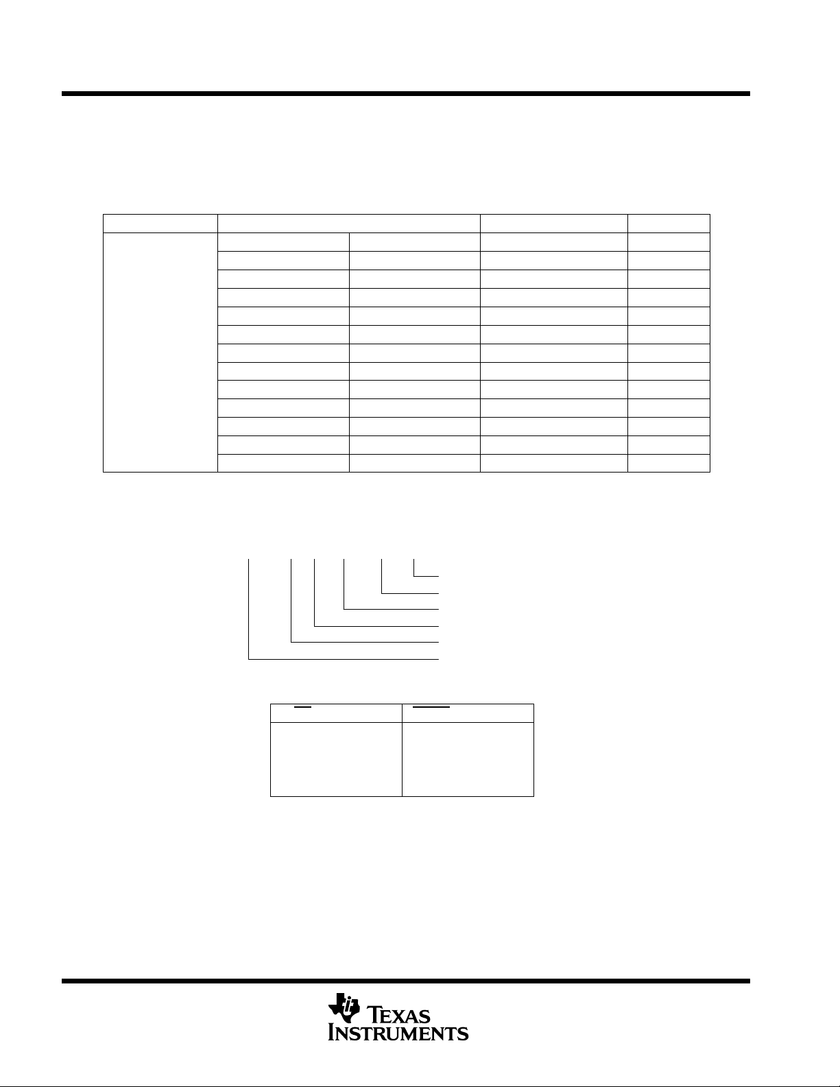
PACKAGE INFORMATION
T
A
TPS3836E18DBVR
TPS3836J25DBVR
TPS3836H30DBVR
TPS3836L30DBVR
TPS3836K33DBVR
TPS3837E18DBVR
–40°C to 85°C
†
The DBVR passive indicates tape and reel of 3000 parts.
‡
The DBVT passive indicates tape and reel of 250 parts.
TPS3837J25DBVR
TPS3837L30DBVR
TPS3837K33DBVR
TPS3838E18DBVR
TPS3838J25DBVR
TPS3838L30DBVR
TPS3838K33DBVR
DEVICE NAME THRESHOLD VOLTAGE SYMBOL
†
TPS3836E18DBVT
†
TPS3836J25DBVT
†
TPS3836H30DBVT
†
TPS3836L30DBVT
†
TPS3836K33DBVT
†
TPS3837E18DBVT
†
TPS3837J25DBVT
†
TPS3837L30DBVT
†
TPS3837K33DBVT
†
TPS3838E18DBVT
†
TPS3838J25DBVT
†
TPS3838L30DBVT
†
TPS3838K33DBVT
‡
‡
‡
‡
‡
‡
‡
‡
‡
‡
‡
‡
‡
1.71 V PDNI
2.25 V PDSI
2.79 V PHRI
2.64 V PCAI
2.93 V PDTI
1.71 V PDOI
2.25 V PDRI
2.64 V PCBI
2.93 V PDUI
1.71 V PDQI
2.25 V PDPI
2.64 V PCCI
2.93 V PDVI
ORDERING INFORMATION
TPS383 6 E 18 DBV R
FUNCTION TABLE TPS3836, TPS3837, TPS3838
MR
L 0 L H
L 1LH
H 0LH
H 1 H L
§
TPS3836 and TPS3838
¶
TPS3837
VDD > V
IT
Reel
Package
Nominal Supply Voltage
Typical Reset Threshold Voltage
Functionality
Family
RESET
§
RESET
¶
2
POST OFFICE BOX 655303 • DALLAS, TEXAS 75265
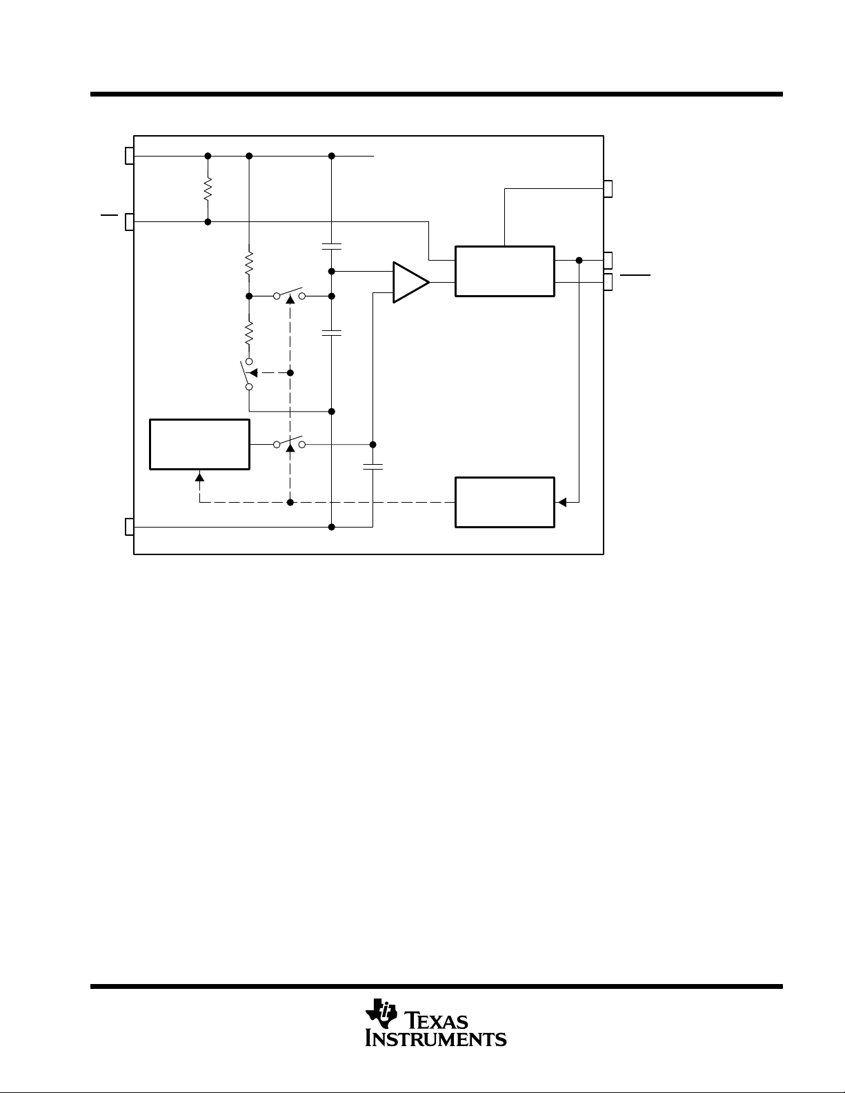
functional block diagram
V
DD
TPS3836E18 / J25 / H30 / L30 / K33
TPS3837E18 / J25 / L30 / K33, TPS3838E18 / J25 / L30 / K33
NANOPOWER SUPERVISORY CIRCUITS
SLVS292A – JUNE 2000 – REVISED JANUARY 2002
MR
GND
R3
Band-Gap
Reference
R1
R2
S2
S1
S3
C1
C2
C3
C
T
+
–
Reset Logic
and Timer
Refresh
Timer
Reset (TPS3837-Push-Pull)
Reset (TPS3836-Push-Pull
TPS3838-Open-Drain)
POST OFFICE BOX 655303 • DALLAS, TEXAS 75265
3
TPS3836E18 / J25 / H30 / L30 / K33
TPS3837E18 / J25 / L30 / K33, TPS3838E18 / J25 / L30 / K33
NANOPOWER SUPERVISORY CIRCUITS
SLVS292A – JUNE 2000 – REVISED JANUARY 2002
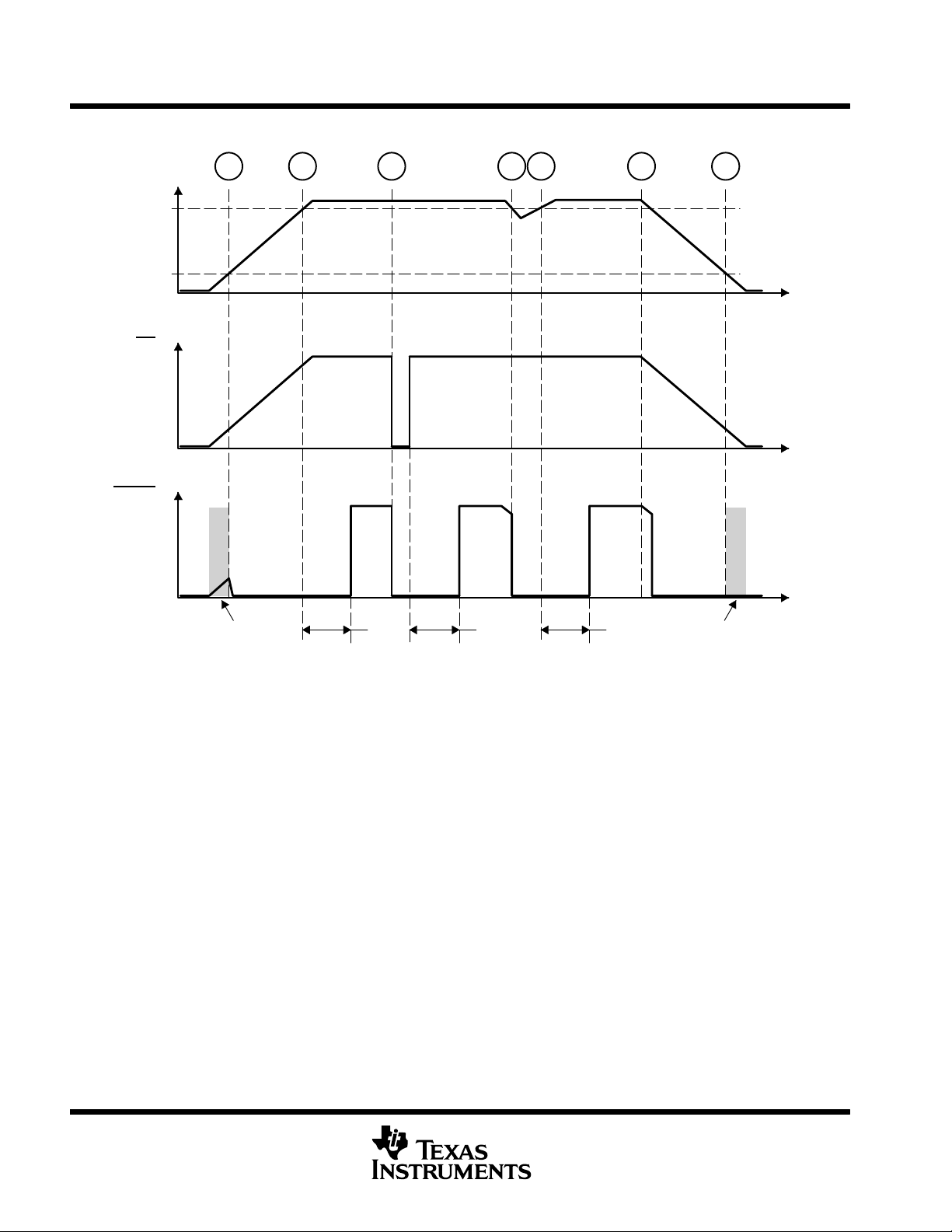
timing diagram
V
DD
< 1.1 V
MR
RESET
A
V
IT
B C D E F G
t
t
t
Undefined
Output
t
d
t
d
t
d
Undefined
Output
4
POST OFFICE BOX 655303 • DALLAS, TEXAS 75265
 Loading...