


 Loading...
TEXAS INSTRUMENTS TPS61010, TPS61011, TPS61012, TPS61013, TPS61014 Technical data
...DGS DRC
TPS61010, TPS61011
TPS61012, TPS61013 TPS61014, TPS61015, TPS61016
www.ti.com |
SLVS314D –SEPTEMBER 2000 –REVISED JUNE 2005 |
|
HIGH-EFFICIENCY, 1-CELL AND 2-CELL BOOST CONVERTERS
FEATURES
∙Integrated Synchronous Rectifier for Highest Power Conversion Efficiency (>95%)
∙Start-Up Into Full Load With Supply Voltages as Low as 0.9 V, Operating Down to 0.8 V
∙200-mA Output Current From 0.9-V Supply
∙Powersave-Mode for Improved Efficiency at Low Output Currents
∙Autodischarge Allows to Discharge Output Capacitor During Shutdown
∙Device Quiescent Current Less Than 50 μA
∙Ease-of-Use Through Isolation of Load From Battery During Shutdown of Converter
∙Integrated Antiringing Switch Across Inductor
∙Integrated Low Battery Comparator
∙Micro-Small 10-Pin MSOP or 3 mm x 3 mm QFN Package
∙EVM Available (TPS6101xEVM-157)
APPLICATIONS
∙All Singleor Dual-Cell Battery Operated Products Like Internet Audio Players, Pager, Portable Medical Diagnostic Equipment, Remote Control, Wireless Headsets
DESCRIPTION
The TPS6101x devices are boost converters intended for systems that are typically operated from a singleor dual-cell nickel-cadmium (NiCd), nickel-metal hydride (NiMH), or alkaline battery.
The converter output voltage can be adjusted from 1.5 V to a maximum of 3.3 V, by an external resistor divider or, is fixed internally on the chip. The devices provide an output current of 200 mA with a supply voltage of only 0.9 V. The converter starts up into a full load with a supply voltage of only 0.9 V and stays in operation with supply voltages down to 0.8 V.
The converter is based on a fixed frequency, current mode, pulse-width-modulation (PWM) controller that goes automatically into power save mode at light load. It uses a built-in synchronous rectifier, so, no external Schottky diode is required and the system efficiency is improved. The current through the switch is limited to a maximum value of 1300 mA. The converter can be disabled to minimize battery drain. During shutdown, the load is completely isolated from the battery.
An autodischarge function allows discharging the output capacitor during shutdown mode. This is especially useful when a microcontroller or memory is supplied, where residual voltage across the output capacitor can cause malfunction of the applications. When programming the ADEN-pin, the autodischarge function can be disabled. A low-EMI mode is implemented to reduce interference and radiated electromagnetic energy when the converter enters the discontinuous conduction mode. The device is packaged in the micro-small space saving 10-pin MSOP package. The TPS61010 is also available in a 3 mm x 3 mm 10-pin QFN package.
|
|
|
L1 |
|
|
|
|
|
|
CIN |
|
10 μH |
|
|
|
|
|
|
|
|
7 |
|
|
|
|
|
|
10 μF |
|
|
|
|
|
|
|
|
|
|
|
|
|
|
|
|
|
|
|
|
SW |
|
|
|
|
|
|
6 |
VBAT |
VOUT 5 |
|
COUT |
VOUT = 3.3 V |
|
|
|
|
|
|
|
R3 |
|
|
|
R1 |
|
|
|
|
22 μF |
|
|
|
|
|
|
|
|
|
||
|
|
|
|
|
|
|
|
|
|
|
9 |
LBI |
LBO 10 |
|
|
Low Battery |
|
|
R2 |
|
TPS61016 |
|
|
|
Warning |
|
|
|
|
|
|
|
|||
|
|
|
|
|
|
|
||
OFF |
ON |
1 |
EN |
FB |
3 |
RC |
|
|
|
|
|
|
|
||||
|
|
|
|
|
|
|||
|
|
|
|
|
|
|
|
|
OFF |
ON |
8 |
|
|
2 |
100 kΩ |
|
|
ADEN |
COMP |
|
|
|
||||
|
|
|
|
|
|
|||
|
|
|
|
|
|
|
||
|
|
|
|
GND |
|
CC1 |
|
CC2 |
|
|
|
|
4 |
|
|
||
|
|
|
|
|
10 pF |
|
10 nF |
|
|
|
|
|
|
|
|
||
Please be aware that an important notice concerning availability, standard warranty, and use in critical applications of Texas Instruments semiconductor products and disclaimers thereto appears at the end of this data sheet.
PRODUCTION DATA information is current as of publication date. |
Copyright © 2000–2005, Texas Instruments Incorporated |
Products conform to specifications per the terms of the Texas |
|
Instruments standard warranty. Production processing does not |
|
necessarily include testing of all parameters. |
|

TPS61010, TPS61011
TPS61012, TPS61013
TPS61014, TPS61015, TPS61016
www.ti.com
SLVS314D –SEPTEMBER 2000 –REVISED JUNE 2005
These devices have limited built-in ESD protection. The leads should be shorted together or the device placed in conductive foam during storage or handling to prevent electrostatic damage to the MOS gates.
AVAILABLE OUTPUT VOLTAGE OPTIONS
T |
OUTPUT VOLTAGE |
PART NUMBER(1) |
MARKING DGS PACKAGE |
PACKAGE(2) |
A |
|
|
|
|
|
Adjustable from 1.5 V to 3.3 V |
TPS61010DGS |
AIP |
|
|
1.5 V |
TPS61011DGS |
AIQ |
|
|
1.8 V |
TPS61012DGS |
AIR |
|
-40°C to 85°C |
2.5 V |
TPS61013DGS |
AIS |
10-Pin MSOP |
2.8 V |
TPS61014DGS |
AIT |
|
|
|
|
|||
|
3.0 V |
TPS61015DGS |
AIU |
|
|
3.3 V |
TPS61016DGS |
AIV |
|
|
Adjustable from 1.5 V to 3.3 V |
TPS61010DRC |
AYA |
10-Pin QFN |
(1)The DGS package and the DRC package are available taped and reeled. Add a R suffix to device type (e.g. TPS61010DGSR or TPS61010DRCR) to order quantities of 3000 devices per reel. The DRC package is also available in mini-reels. Add a T suffix to the device type (e.g. TPS61010DRCT) to order quantities of 250 devices per reel.
(2)For the most current package and ordering information, see the Package Option Addendum at the end of this document, or see the TI Web site at www.ti.com.
ABSOLUTE MAXIMUM RATINGS
over operating free-air temperature range (unless otherwise noted)(1)
|
|
UNIT |
Input voltage range: |
VBAT, VOUT, EN, LBI, FB, ADEN |
-0.3 V to 3.6 V |
|
SW |
-0.3 V to 7 V |
Voltage range: |
LBO, COMP |
-0.3 V to 3.6 V |
Operating free-air temperature range, TA |
-40°C to 85°C |
|
Maximum junction temperature, TJ |
150°C |
|
Storage temperature range, Tstg |
-65°C to 150°C |
|
Lead temperature 1,6 mm (1/16 inch) from case for 10s |
260°C |
|
(1)Stresses beyond those listed under "absolute maximum ratings" may cause permanent damage to the device. These are stress ratings only, and functional operation of the device at these or any other conditions beyond those indicated under "recommended operating conditions" is not implied. Exposure to absolute-maximum-rated conditions for extended periods may affect device reliability.
DISSIPATION RATING TABLE
PACKAGE |
TA <25°C |
DERATING FACTOR |
TA = 70°C |
TA = 85°C |
|
POWER RATING |
ABOVE TA = 25°C |
POWER RATING |
POWER RATING |
DGS |
424 mW |
3.4 mW/°C |
271 mW |
220 mW |
RECOMMENDED OPERATING CONDITIONS
|
MIN |
NOM |
MAX |
UNIT |
Supply voltage at VBAT, VI |
0.8 |
|
VOUT |
V |
Maximum output current at VIN = 1.2 V, IO |
100 |
|
|
mA |
Maximum output current at VIN = 2.4 V, IO |
200 |
|
|
mA |
Inductor, L1 |
10 |
33 |
|
µH |
Input capacitor, CI |
|
10 |
|
µF |
Output capacitor, Co |
10 |
22 |
47 |
µF |
Operating virtual junction temperature, TJ |
-40 |
|
125 |
°C |
2

TPS61010, TPS61011 TPS61012, TPS61013
TPS61014, TPS61015, TPS61016
www.ti.com
SLVS314D –SEPTEMBER 2000 –REVISED JUNE 2005
ELECTRICAL CHARACTERISTICS
over recommended operating free-air temperature range, VBAT = 1.2 V, EN = VBAT (unless otherwise noted)
 PARAMETER
|
Minimum input voltage for |
VI |
start-up |
|
Input voltage once started |
|
Programmable output |
|
voltage range |
VO
Output voltage
IO |
Maximum continuous output |
|
current |
||
I(SW) |
Switch current limit |
|
V(FB) |
Feedback voltage |
|
f |
Oscillator frequency |
|
D |
Maximum duty cycle |
|
rDS(on) |
NMOS switch on-resistance |
|
PMOS switch on-resistance |
||
|
||
rDS(on) |
NMOS switch on-resistance |
|
PMOS switch on-resistance |
||
|
||
|
Line regulation (1) |
|
|
Load regulation (1) |
|
|
Autodischarge switch |
|
|
resistance |
|
|
Residual output voltage |
|
|
after autodischarge |
|
V |
LBI voltage threshold (2) |
|
IL |
|
|
|
LBI input hysteresis |
|
|
LBI input current |
|
VOL |
LBO output low voltage |
|
|
LBO output leakage current |
|
I(FB) |
FB input bias current |
|
(TPS61010 only) |
||
VIL |
EN and ADEN input low |
|
voltage |
TEST CONDITIONS |
MIN |
TYP |
MAX |
UNIT |
||
RL = 33 Ω |
|
0.85 |
0.9 |
|
||
RL = 3 kΩ, TA = 25 °C |
0.8 |
|
|
V |
||
IO = 100 mA |
0.8 |
|
|
|
||
TPS61010, IOUT = 100 mA |
1.5 |
|
3.3 |
V |
||
TPS61011, 0.8 V < VI < VO, IO = 0 to 100 mA |
1.45 |
1.5 |
1.55 |
V |
||
TPS61012, 0.8 V < VI < VO, IO = 0 to 100 mA |
1.74 |
1.8 |
1.86 |
|||
|
||||||
TPS61013, 0.8 V < VI < VO, IO = 0 to 100 mA |
2.42 |
2.5 |
2.58 |
V |
||
TPS61013, 1.6 V < VI < VO, IO = 0 to 200 mA |
2.42 |
2.5 |
2.58 |
V |
||
TPS61014, 0.8 V < VI < VO, IO = 0 to 100 mA |
2.72 |
2.8 |
2.88 |
V |
||
TPS61014, 1.6 V < VI < VO, IO = 0 to 200 mA |
2.72 |
2.8 |
2.88 |
V |
||
TPS61015, 0.8 V < VI < VO, IO = 0 to 100 mA |
2.9 |
3.0 |
3.1 |
V |
||
TPS61015, 1.6 V < VI < VO, IO = 0 to 200 mA |
2.9 |
3.0 |
3.1 |
V |
||
TPS61016, 0.8 V < VI < VO, IO = 0 to 100 mA |
3.2 |
3.3 |
3.4 |
V |
||
TPS61016, 1.6 V < VI < VO, IO = 0 to 200 mA |
3.2 |
3.3 |
3.4 |
V |
||
VI |
> 0.8 V |
100 |
|
|
mA |
|
VI |
> 1.8 V |
250 |
|
|
||
|
|
|
||||
TPS61011, once started |
0.39 |
0.48 |
|
|
||
TPS61012, once started |
0.54 |
0.56 |
|
|
||
TPS61013, once started |
0.85 |
0.93 |
|
A |
||
TPS61014, once started |
0.95 |
1.01 |
|
|||
|
|
|||||
TPS61015, once started |
1 |
1.06 |
|
|
||
TPS61016, once started |
1.07 |
1.13 |
|
|
||
|
|
480 |
500 |
520 |
mV |
|
|
|
420 |
500 |
780 |
kHz |
|
|
|
|
85% |
|
|
|
VO = 1.5 V |
|
0.37 |
0.51 |
Ω |
||
|
0.45 |
0.54 |
||||
|
|
|
|
|||
VO = 3.3 V |
|
0.2 |
0.37 |
Ω |
||
|
0.3 |
0.45 |
||||
|
|
|
|
|||
VI = 1.2 V to 1.4 V, IO = 100 mA |
|
0.3 |
|
%/V |
||
VI = 1.2 V; IO = 50 mA to 100 mA |
|
0.1 |
|
|||
|
|
|
||||
|
|
|
300 |
400 |
Ω |
|
ADEN = VBAT; EN = GND |
|
|
0.4 |
V |
||
V(LBI) voltage decreasing |
480 |
500 |
520 |
mV |
||
|
|
|
10 |
|
mv |
|
|
|
|
0.01 |
0.03 |
|
|
V(LBI) = 0 V, VO = 3.3 V, I(OL) = 10 µA |
|
0.04 |
0.2 |
V |
||
V(LBI) = 650 mV, V(LBO) = VO |
|
|
0.03 |
µA |
||
V(FB) = 500 mV |
|
0.01 |
0.03 |
|
||
0.8 V < VBAT < 3.3 V |
|
|
0.2 × VBAT |
V |
||
(1)Line and load regulation is measured as a percentage deviation from the nominal value (i.e., as percentage deviation from the nominal output voltage). For line regulation, x %/V stands for ±x% change of the nominal output voltage per 1-V change on the input/supply voltage. For load regulation, y% stands for ±y% change of the nominal output voltage per the specified current change.
(2)For proper operation the voltage at LBI may not exceed the voltage at VBAT.
3

TPS61010, TPS61011
TPS61012, TPS61013
TPS61014, TPS61015, TPS61016
www.ti.com
SLVS314D –SEPTEMBER 2000 –REVISED JUNE 2005
ELECTRICAL CHARACTERISTICS (continued)
over recommended operating free-air temperature range, VBAT = 1.2 V, EN = VBAT (unless otherwise noted)
PARAMETER |
TEST CONDITIONS |
|
||
VIH |
EN and ADEN input high |
0.8 V < VBAT < 3.3 V |
|
|
voltage |
|
|||
|
EN and ADEN input current |
EN and ADEN = GND or VBAT |
||
Iq |
Quiescent current into pins |
IL = 0 mA, VEN = VI |
VBAT/SW |
|
VBAT/SW and VOUT |
VO |
|||
|
|
|||
Ioff |
Shutdown current from |
VEN = 0 V, ADEN = VBAT, TA= 25°C |
||
power source |
||||
MIN |
TYP |
MAX |
|
UNIT |
0.8 ×VBAT |
|
|
|
V |
|
0.01 |
|
0.03 |
µA |
|
31 |
|
46 |
µA |
|
5 |
|
8 |
|
|
|
|
||
|
1 |
|
3 |
µA |
FUNCTIONAL BLOCK DIAGRAMS
fixed output voltage versions TPS61011 to TPS61016
|
|
L1 |
|
|
|
|
|
|
|
|
|
SW |
|
|
|
CIN |
|
|
|
|
|
|
|
|
Antiringing |
|
|
|
Bias |
|
|
|
_ |
|
|
Control |
|
||
|
Comparator |
|
|
|
|
|
|
|
and Switch |
+ |
|
|
|
VOUT |
|
VBAT |
|
|
|
|
|
|
COUT |
|
|
|
|
|
|
|
|
|
|
|
|
|
ADEN |
|
|
|
UVLO |
|
|
|
|
|
|
|
|
|
Control Logic |
Current Sense, |
|
|
|
EN |
|
|
Oscillator |
Current Limit, Slope |
|
||
|
|
|
Gate Drive |
Compensation |
|
|
|
ADEN |
ADEN |
|
|
|
|
|
|
LBI |
|
|
+ |
|
_ |
|
FB |
|
|
_ |
|
|
|
||
|
|
|
|
Bandgap |
|
||
|
_ |
|
Error |
Error |
+ |
|
|
|
Comparator |
Reference |
|
||||
LBO |
|
Amplifier |
|
|
|||
+ |
VREF |
|
|
|
|
||
|
|
|
|
|
|
||
|
|
|
GND |
COMP |
|
|
|
4

TPS61010, TPS61011 TPS61012, TPS61013
TPS61014, TPS61015, TPS61016
www.ti.com
SLVS314D –SEPTEMBER 2000 –REVISED JUNE 2005
FUNCTIONAL BLOCK DIAGRAMS (continued)
adjustable output voltage version TPS61010
|
|
L1 |
|
|
|
|
|
|
|
|
|
SW |
|
|
|
CIN |
|
|
|
|
|
|
|
|
Antiringing |
|
|
|
Bias |
|
|
|
_ |
|
|
Control |
|
||
|
Comparator |
|
|
|
|
|
|
|
and Switch |
+ |
|
|
|
VOUT |
|
VBAT |
|
|
|
|
|
|
COUT |
|
|
|
|
|
|
|
|
|
|
|
|
|
ADEN |
|
|
|
UVLO |
|
|
|
|
|
|
|
|
|
Control Logic |
Current Sense, |
|
|
|
EN |
|
|
Oscillator |
Current Limit, Slope |
|
||
|
|
|
Gate Drive |
Compensation |
|
|
|
ADEN |
ADEN |
|
|
|
|
|
|
LBI |
|
|
+ |
|
_ |
|
FB |
|
|
_ |
|
|
Bandgap |
|
|
|
_ |
|
Error |
Error |
+ |
|
|
|
Comparator |
Reference |
|
||||
LBO |
|
Amplifier |
|
|
|||
+ |
VREF |
|
|
|
|
||
|
|
|
|
|
|
||
|
|
|
GND |
COMP |
|
|
|
5

TPS61010, TPS61011
TPS61012, TPS61013
TPS61014, TPS61015, TPS61016
www.ti.com
SLVS314D –SEPTEMBER 2000 –REVISED JUNE 2005 |
|
|
|
||
|
|
DGS |
|
|
DRC |
|
|
(TOP VIEW) |
|
|
|
|
|
|
|
(TOP VIEW) |
|
|
|
|
|
|
|
EN |
1 |
10 |
LBO |
EN |
LBO |
COMP |
2 |
9 |
LBI |
COMP |
LBI |
FB |
3 |
8 |
ADEN |
FB |
ADEN |
GND |
4 |
7 |
SW |
GND |
SW |
VOUT |
5 |
6 |
VBAT |
VOUT |
VBAT |
Terminal Functions
|
Terminal |
|
|
|
|
Name |
DRG |
DRC |
I/O |
Description |
|
No. |
No. |
|
|
||
|
|
|
|||
ADEN |
8 |
8 |
I |
Autodischarge input. The autodischarge function is enabled if this pin is connected to VBAT, it is disabled |
|
if ADEN is tied to GND. |
|||||
|
|
|
|
||
COMP |
2 |
2 |
I |
Compensation of error amplifier. Connect an R/C/C network to set frequency response of control loop. |
|
EN |
1 |
1 |
I |
Chip-enable input. The converter is switched on if this pin is set high, it is switched off if this pin is |
|
|
|
connected to GND. |
|||
|
|
|
|
||
|
|
|
|
Feedback input for adjustable output voltage version TPS61010. Output voltage is programmed |
|
FB |
3 |
3 |
I |
depending on the output voltage divider connected there. For the fixed output voltage versions, leave |
|
|
|
|
|
FB-pin unconnected. |
|
GND |
4 |
4 |
|
Ground |
|
|
|
|
|
Low-battery detector input. A low battery warning is generated at LBO when the voltage on LBI drops |
|
LBI |
9 |
9 |
I |
below the threshold of 500 mV. Connect LBI to GND or VBAT if the low-battery detector function is not |
|
|
|
|
|
used. Do not leave this pin floating. |
|
LBO |
10 |
10 |
O |
Open-drain low-battery detector output. This pin is pulled low if the voltage on LBI drops below the |
|
threshold of 500 mV. A pullup resistor must be connected between LBO and VOUT. |
|||||
|
|
|
|
||
SW |
7 |
7 |
I |
Switch input pin. The inductor is connected to this pin. |
|
VOUT |
5 |
5 |
O |
Output voltage. Internal resistor divider sets regulated output voltage in fixed output voltage versions. |
|
VBAT |
6 |
6 |
I |
Supply pin |
DETAILED DESCRIPTION
Controller Circuit
The device is based on a current-mode control topology using a constant frequency pulse-width modulator to regulate the output voltage. The controller limits the current through the power switch on a pulse by pulse basis. The current-sensing circuit is integrated in the device, therefore, no additional components are required. Due to the nature of the boost converter topology used here, the peak switch current is the same as the peak inductor current, which will be limited by the integrated current limiting circuits under normal operating conditions.
The control loop must be externally compensated with an R-C-C network connected to the COMP-pin.
Synchronous Rectifier
The device integrates an N-channel and a P-channel MOSFET transistor to realize a synchronous rectifier. There
is no additional Schottky diode required. Because the device uses a integrated low rDS(on) PMOS switch for rectification, the power conversion efficiency reaches 95%.
A special circuit is applied to disconnect the load from the input during shutdown of the converter. In conventional synchronous rectifier circuits, the backgate diode of the high-side PMOS is forward biased in shutdown and allows current flowing from the battery to the output. This device, however, uses a special circuit to disconnect the backgate diode of the high-side PMOS and so, disconnects the output circuitry from the source when the regulator is not enabled (EN = low).
The benefit of this feature for the system design engineer, is that the battery is not depleted during shutdown of the converter. So, no additional effort has to be made by the system designer to ensure disconnection of the battery from the output of the converter. Therefore, design performance will be increased without additional costs and board space.
6

TPS61010, TPS61011 TPS61012, TPS61013
TPS61014, TPS61015, TPS61016
www.ti.com
SLVS314D –SEPTEMBER 2000 –REVISED JUNE 2005
DETAILED DESCRIPTION (continued)
Power-Save Mode
The TPS61010 is designed for high efficiency over a wide output current range. Even at light loads, the efficiency stays high because the switching losses of the converter are minimized by effectively reducing the switching frequency. The controller enters a powersave-mode if certain conditions are met. In this mode, the controller only switches on the transistor if the output voltage trips below a set threshold voltage. It ramps up the output voltage with one or several pulses, and goes again into powersave-mode once the output voltage exceeds a set threshold voltage.
Device Enable
The device is shut down when EN is set to GND. In this mode, the regulator stops switching, all internal control circuitry including the low-battery comparator, is switched off, and the load is disconnected from the input (as described above in the synchronous rectifier section). This also means that the output voltage may drop below the input voltage during shutdown.
The device is put into operation when EN is set high. During start-up of the converter, the duty cycle is limited in order to avoid high peak currents drawn from the battery. The limit is set internally by the current limit circuit and is proportional to the voltage on the COMP-pin.
Under-Voltage Lockout
An under-voltage lockout function prevents the device from starting up if the supply voltage on VBAT is lower than approximately 0.7 V. This under-voltage lockout function is implemented in order to prevent the malfunctioning of the converter. When in operation and the battery is being discharged, the device will automatically enter the shutdown mode if the voltage on VBAT drops below approximately 0.7 V.
Autodischarge
The autodischarge function is useful for applications where the supply voltage of a μC, μP, or memory has to be removed during shutdown in order to ensure a defined state of the system.
The autodischarge function is enabled when the ADEN is set high, and is disabled when the ADEN is set to GND. When the autodischarge function is enabled, the output capacitor will be discharged after the device is shut down by setting EN to GND. The capacitors connected to the output are discharged by an integrated switch of 300 Ω, hence the discharge time depends on the total output capacitance. The residual voltage on VOUT is less than 0.4 V after autodischarge.
Low-Battery Detector Circuit (LBI and LBO)
The low-battery detector circuit is typically used to supervise the battery voltage and to generate an error flag when the battery voltage drops below a user-set threshold voltage. The function is active only when the device is enabled. When the device is disabled, the LBO-pin is high impedance. The LBO-pin goes active low when the voltage on the LBI-pin decreases below the set threshold voltage of 500 mV ±15 mV, which is equal to the internal reference voltage. The battery voltage, at which the detection circuit switches, can be programmed with a resistive divider connected to the LBI-pin. The resistive divider scales down the battery voltage to a voltage level of 500 mV, which is then compared to the LBI threshold voltage. The LBI-pin has a built-in hysteresis of 10 mV. See the application section for more details about the programming of the LBI-threshold.
If the low-battery detection circuit is not used, the LBI-pin should be connected to GND (or to VBAT) and the LBO-pin can be left unconnected. Do not let the LBI-pin float.
Antiringing Switch
The device integrates a circuit that removes the ringing that typically appears on the SW-node when the converter enters the discontinuous current mode. In this case, the current through the inductor ramps to zero and the integrated PMOS switch turns off to prevent a reverse current from the output capacitors back to the battery. Due to remaining energy that is stored in parasitic components of the semiconductors and the inductor, a ringing on the SW pin is induced. The integrated antiringing switch clamps this voltage internally to VBAT and therefore, dampens this ringing.
7
TPS61010, TPS61011
TPS61012, TPS61013
TPS61014, TPS61015, TPS61016
www.ti.com
SLVS314D –SEPTEMBER 2000 –REVISED JUNE 2005
DETAILED DESCRIPTION (continued)
Adjustable Output Voltage
The devices with fixed output voltages are trimmed to operate with an output voltage accuracy of ±3%.
The accuracy of the adjustable version is determined by the accuracy of the internal voltage reference, the controller topology, and the accuracy of the external resistor. The reference voltage has an accuracy of ±4% over line, load, and temperature. The controller switches between fixed frequency and pulse-skip mode, depending on load current. This adds an offset to the output voltage that is equivalent to 1% of VO. The tolerance of the resistors in the feedback divider determine the total system accuracy.
Parameter Measurement Information
|
|
L1 |
|
|
|
|
|
|
CIN |
10 μH |
|
|
|
|
|
|
|
7 |
|
|
|
|
|
|
10 μF |
|
|
|
|
|
|
|
|
SW |
|
|
|
|
|
|
|
|
|
|
|
|
|
|
6 |
VBAT |
VOUT 5 |
|
|
VOUT = 3.3 V |
|
|
|
|
|
|
R3 |
COUT |
|
|
|
|
|
|
22 |
μ |
|
R1 |
|
|
|
|
|
F |
|
9 |
|
LBO 10 |
|
|
|
||
|
LBI |
|
|
Low Battery Warning |
|||
R2 |
|
TPS61016 |
|
|
|
|
|
|
8 |
ADEN |
FB |
3 |
RC |
|
|
|
|
|
|
||||
|
|
|
|
|
|
|
|
OFF |
ON 1 |
EN |
COMP 2 |
100 kΩ |
|
|
|
|
|
|
|||||
|
|
|
|
||||
|
|
|
GND |
|
CC1 |
|
CC2 |
|
|
|
4 |
|
|
||
|
|
|
|
10 pF |
|
10 nF |
|
|
|
|
|
|
|
||
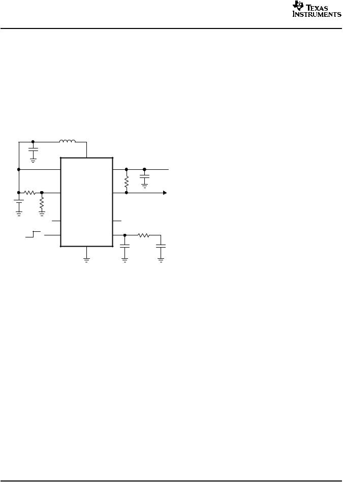
List of Components:
IC1: Only Fixed Output Versions
(Unless Otherwise Noted)
L1: SUMIDA CDRH6D38 – 100
CIN: X7R/X5R Ceramic
COUT : X7R/X5R Ceramic
Figure 1. Circuit Used for Typical Characteristics Measurements
8

TPS61010, TPS61011 TPS61012, TPS61013
TPS61014, TPS61015, TPS61016
www.ti.com
|
SLVS314D –SEPTEMBER 2000 –REVISED JUNE 2005 |
||
|
Typical Characteristics |
|
|
Table of Graphs |
|
|
|
|
|
FIGURE |
|
Maximum output current |
vs Input voltage for VO = 2.5 V, 3.3 V |
3 |
|
vs Input voltage for VO = 1.5 V, 1.8 V |
4 |
||
|
|||
|
vs Output current for VI = 1.2 VVO = 1.5 V, L1 = Sumida CDR74 - 10 µH |
5 |
|
|
vs Output current for VI = 1.2 VVO = 2.5 V, L1 = Sumida CDR74 - 10 µH |
6 |
|
|
vs Output current for VIN = 1.2 VVO = 3.3 V, L1 = Sumida CDR74 - 10 µH |
7 |
|
|
vs Output current for VI = 2.4 VVO = 3.3 V, L1 = Sumida CDR74 - 10 µH |
8 |
|
|
vs Input voltage for IO = 10 mA, IO = 100 mA, IO = 200 mAVO = 3.3 V, L1 = |
9 |
|
|
Sumida CDR74 - 10 µH |
|
|
|
TPS61016, VBAT = 1.2 V, IO = 100 mA |
|
|
|
Sumida CDRH6D38 - 10 µH |
|
|
|
Sumida CDRH5D18 - 10 µH |
|
|
|
Sumida CDRH74 - 10 µH |
|
|
Efficiency |
Sumida CDRH74B - 10 µH |
|
|
|
Coilcraft DS 1608C - 10 µH |
|
|
|
Coilcraft DO 1608C - 10 µH |
|
|
|
Coilcraft DO 3308P - 10 µH |
10 |
|
|
Coilcraft DS 3316 - 10 µH |
|
|
|
Coiltronics UP1B - 10 µH |
|
|
|
Coiltronics UP2B - 10 µH |
|
|
|
Murata LQS66C - 10 µH |
|
|
|
Murata LQN6C - 10 µH |
|
|
|
TDK SLF 7045 - 10 µH |
|
|
|
TDK SLF 7032 - 10 µH |
|
|
|
vs Output current TPS61011 |
11 |
|
Output voltage |
vs Output current TPS61013 |
12 |
|
|
vs Output current TPS61016 |
13 |
|
Minimum supply start-up voltage |
vs Load resistance |
14 |
|
No-load supply current |
vs Input voltage |
15 |
|
Shutdown supply current |
vs Input voltage |
16 |
|
Switch current limit |
vs Output voltage |
17 |
|
|
Output voltage (ripple) in continuous modeInductor current |
18 |
|
|
Output voltage (ripple) in discontinuous modeInductor current |
19 |
|
Waveforms |
Load transient response for output current step of 50 mA to 100 mA |
20 |
|
Line transient response for supply voltage step from 1.08 V to 1.32 V at |
21 |
||
|
|||
|
IO = 100 mA |
|
|
|
Converter start-up time after enable |
22 |
|
9
Loading...