


Texas Instruments TPS2815PWLE, TPS2815PWR, TPS2815P, TPS2815DR, TPS2814PWR Datasheet
...TPS2811, TPS2812, TPS2813, TPS2814, TPS2815 |
||||||||||
|
DUAL HIGH-SPEED MOSFET DRIVERS |
|||||||||
|
SLVS132D ± NOVEMBER 1995 ± REVISED NOVEMBER 1997 |
|||||||||
|
|
|
|
|
|
|
|
|
|
|
D Industry-Standard Driver Replacement |
TPS2811, TPS2812, TPS2813 . . . D, P, AND PW |
|||||||||
D 25-ns Max Rise/Fall Times and 40-ns Max |
|
|
|
|
|
|
PACKAGES |
|
|
|
|
|
|
|
|
|
(TOP VIEW) |
|
|
||
Propagation Delay ± 1-nF Load, VCC = 14 V |
|
|
|
|
|
|
|
|
||
REG_IN |
|
|
|
|
REG_OUT |
|||||
|
|
|
|
|||||||
D 2-A Peak Output Current, VCC = 14 V |
|
|
1 |
8 |
||||||
D 5-μA Supply Current Ð Input High or Low |
|
1IN |
|
|
2 |
7 |
1OUT |
|||
D 4-V to 14-V Supply-Voltage Range; Internal |
GND |
|
|
3 |
6 |
VCC |
||||
|
2IN |
|
|
4 |
5 |
2OUT |
||||
Regulator Extends Range to 40 V (TPS2811, |
|
|
||||||||
|
|
|
|
|
|
|
|
|
|
|
TPS2812, TPS2813) |
TPS2814 . . . D, P, AND PW PACKAGES |
|||||||||
D ±40°C to 125°C Ambient-Temperature |
||||||||||
Operating Range |
|
|
|
|
|
|
(TOP VIEW) |
|
|
|
|
|
|
|
|
|
|
|
|
|
|
description |
|
1IN1 |
|
1 |
8 |
GND |
||||
|
|
|||||||||
|
|
|
|
|
|
|
|
|
|
|
|
1IN2 |
|
|
2 |
7 |
1OUT |
||||
|
|
|
||||||||
The TPS28xx series of dual high-speed MOSFET |
|
2IN1 |
|
|
3 |
6 |
VCC |
|||
drivers are capable of delivering peak currents of |
|
2IN2 |
|
|
|
4 |
5 |
2OUT |
||
2 A into highly capacitive loads. This performance |
|
|
|
|
|
|
|
|
|
|
|
|
|
|
|
|
|
|
|
|
|
is achieved with a design that inherently |
TPS2815 . . . D, P, AND PW PACKAGES |
|||||||||
minimizes shoot-through current and consumes |
|
|
|
|
|
|
(TOP VIEW) |
|
|
|
an order of magnitude less supply current than |
|
1IN1 |
|
|
|
|
GND |
|||
|
|
|
|
|
||||||
competitive products. |
|
|
1 |
8 |
||||||
The TPS2811, TPS2812, and TPS2813 drivers |
|
1IN2 |
|
|
2 |
7 |
1OUT |
|||
|
2IN1 |
|
|
3 |
6 |
VCC |
||||
include a regulator to allow operation with supply |
|
|
||||||||
|
2IN2 |
|
|
4 |
5 |
2OUT |
||||
inputs between 14 V and 40 V. The regulator |
|
|
||||||||
|
|
|
|
|
|
|
|
|
|
|
output can power other circuitry, provided power |
|
|
|
|
|
|
|
|
|
|
dissipation does not exceed package limitations. When the regulator is not required, REG_IN and REG_OUT can be left disconnected or both can be connected to VCC or GND.
The TPS2814 and the TPS2815 have 2-input gates that give the user greater flexibility in controlling the MOSFET. The TPS2814 has AND input gates with one inverting input. The TPS2815 has dual-input NAND gates.
TPS28xx series drivers, available in 8-pin PDIP, SOIC, and TSSOP packages and as unmounted ICs, operate over a ambient temperature range of ±40°C to 125°C.
AVAILABLE OPTIONS
|
|
|
PACKAGED DEVICES |
CHIP |
||
|
INTERNAL |
|
|
|
|
|
|
|
SMALL |
PLASTIC |
|
||
TA |
LOGIC FUNCTION |
|
FORM |
|||
REGULATOR |
OUTLINE |
DIP |
TSSOP (PW) |
|||
|
|
|
(D) |
(P) |
|
(Y) |
|
|
|
|
|
||
|
|
|
|
|
|
|
|
|
Dual inverting drivers |
TPS2811D |
TPS2811P |
TPS2811PWLE |
TPS2811Y |
± 40°C |
Yes |
Dual noninverting drivers |
TPS2812D |
TPS2812P |
TPS2812PWLE |
TPS2812Y |
|
One inverting and one noninverting driver |
TPS2813D |
TPS2813P |
TPS2813PWLE |
TPS2813Y |
|
to |
|
|||||
|
|
|
|
|
|
|
|
Dual 2-input AND drivers, one inverting input on |
TPS2814D |
TPS2814P |
TPS2814PWLE |
TPS2814Y |
|
125°C |
|
|||||
|
No |
each driver |
|
|
|
|
|
|
Dual 2-input NAND drivers |
TPS2815D |
TPS2815P |
TPS2815PWLE |
TPS2815Y |
|
|
|
|
|
|
|
The D package is available taped and reeled. Add R suffix to device type (e.g., TPS2811DR). The PW package is only available left-end taped and reeled and is indicated by the LE suffix on the device type (e.g., TPS2811PWLE).
Please be aware that an important notice concerning availability, standard warranty, and use in critical applications of Texas Instruments semiconductor products and disclaimers thereto appears at the end of this data sheet.
PRODUCTION DATA information is current as of publication date. Products conform to specifications per the terms of Texas Instruments standard warranty. Production processing does not necessarily include testing of all parameters.
Copyright 1997, Texas Instruments Incorporated
POST OFFICE BOX 655303 •DALLAS, TEXAS 75265 |
1 |
TPS2811, TPS2812, TPS2813, TPS2814, TPS2815 DUAL HIGH-SPEED MOSFET DRIVERS
SLVS132D ± NOVEMBER 1995 ± REVISED NOVEMBER 1997
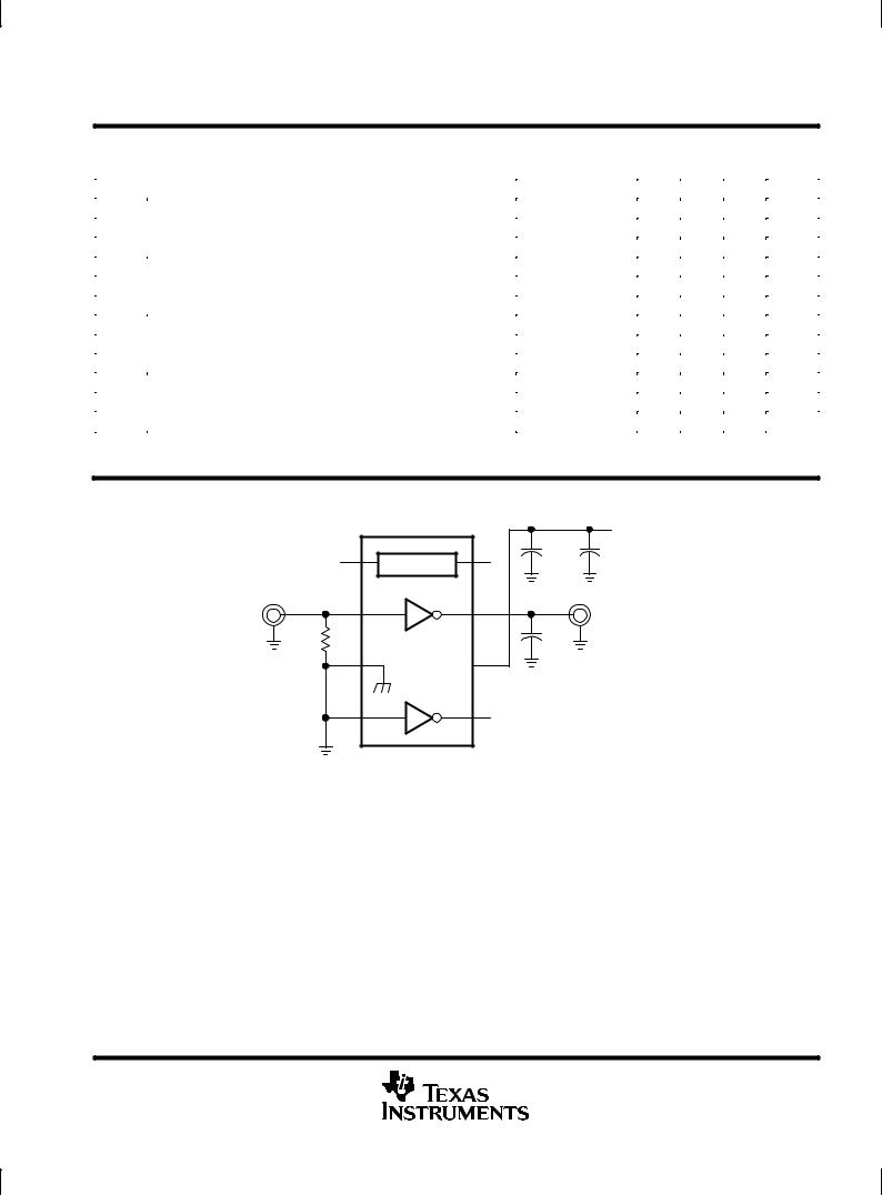
functional block diagram
|
|
TPS2811 |
REG_IN |
1 |
Regulator |
|
||
1IN |
2 |
|
|
|
|
2IN |
4 |
|
3 |
|
|
GND |
|
|
|
|
|
|
|
TPS2812 |
REG_IN |
1 |
Regulator |
|
||
1IN |
2 |
|
|
|
|
2IN |
4 |
|
|
|
|
GND |
3 |
|
|
|
|
|
|
TPS2813 |
REG_IN |
1 |
Regulator |
|
||
1IN |
2 |
|
|
|
|
2IN |
4 |
|
|
|
|
GND |
3 |
|
|
|
|
|
|
TPS2814 |
1IN1 |
1 |
|
2 |
|
|
1IN2 |
|
|
|
|
|
2IN1 |
3 |
|
4 |
|
|
2IN2 |
|
|
|
|
|
GND |
8 |
|
|
|
|
|
|
TPS2815 |
1IN1 |
1 |
|
2 |
|
|
1IN2 |
|
|
|
|
|
2IN1 |
3 |
|
4 |
|
|
2IN2 |
|
|
8 |
|
|
GND |
|
|
|
|
8
REG_OUT
6
VCC
7
1OUT
5
2OUT
8
REG_OUT
6
VCC
7
1OUT
5
2OUT
8
REG_OUT
6
VCC
7
1OUT
5
2OUT
6
VCC
7
1OUT
5
2OUT
6
VCC
7
1OUT
5
2OUT
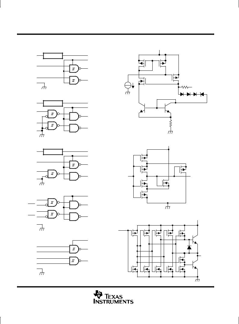
regulator diagram (TPS2811, TPS2812, TPS2813 only)
REG_IN
7.5 Ω |
REG_OUT |
input stage diagram
VCC
IN
To Drive
Stage
output stage diagram
VCC
Predrive
OUT
2 |
POST OFFICE BOX 655303 •DALLAS, TEXAS 75265 |
TPS2811, TPS2812, TPS2813, TPS2814, TPS2815
DUAL HIGH-SPEED MOSFET DRIVERS
SLVS132D ± NOVEMBER 1995 ± REVISED NOVEMBER 1997
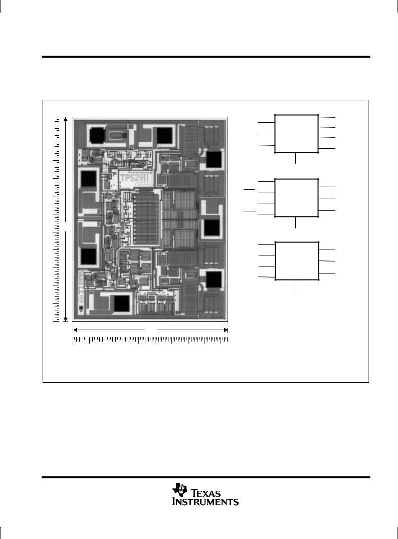
TPS28xxY chip information
This chip, when properly assembled, displays characteristics similar to those of the TPS28xx. Thermal compression or ultrasonic bonding may be used on the doped aluminum bonding pads. The chip may be mounted with conductive epoxy or a gold-silicon preform.
|
BONDING PAD ASSIGNMENTS |
|
|
|
(8) |
|
|
|
(1) |
|
REG_OUT |
|
|
|
REG_IN |
TPS2811Y |
(7) |
|
|
|
(2) |
1OUT |
|
|
|
|
TPS2812Y |
(6) |
|
(1) |
(8) |
|
1IN |
||
|
TPS2813Y |
VCC |
|||
|
|
|
(4) |
||
|
|
|
|
(5) |
|
|
|
|
2IN |
|
|
|
|
|
|
2OUT |
|
|
|
|
|
|
|
|
|
(7) |
|
(3) |
|
|
|
|
|
|
|
|
|
|
|
GND |
|
(2) |
|
|
(1) |
|
(7) |
|
|
1IN1 |
|
||
|
|
|
(2) |
|
1OUT |
|
|
|
1IN2 |
|
(6) |
|
|
|
(3) |
TPS2814Y |
VCC |
|
|
|
2IN1 |
|
(5) |
|
|
|
(4) |
|
|
|
|
|
|
2OUT |
|
|
|
|
2IN2 |
|
|
57 |
|
|
|
(8) |
|
|
(6) |
|
GND |
|
|
|
|
|
|
||
|
|
|
|
|
|
|
|
|
(1) |
|
(7) |
|
|
|
1IN1 |
|
|
|
|
|
(2) |
|
1OUT |
(3) |
|
|
1IN2 |
TPS2815Y |
(6) |
|
|
|
(3) |
VCC |
|
|
|
|
2IN1 |
|
(5) |
|
|
|
(4) |
|
|
|
|
|
|
2OUT |
|
|
|
(5) |
2IN2 |
|
|
|
|
|
(8) |
|
|
|
|
|
|
|
|
|
|
|
|
GND |
|
|
(4) |
|
CHIP THICKNESS: 15 MILS TYPICAL |
||
|
|
|
|||
|
|
|
BONDING PADS: 4 × 4 MILS MINIMUM |
||
|
47 |
|
TJmax OPERATING TEMPERATURE = 150°C |
||
|
|
|
|||
|
|
|
TOLERANCES ARE ± 10%. |
|
|
|
|
|
ALL DIMENSIONS ARE IN MILS. |
||
POST OFFICE BOX 655303 •DALLAS, TEXAS 75265 |
3 |
TPS2811, TPS2812, TPS2813, TPS2814, TPS2815
DUAL HIGH-SPEED MOSFET DRIVERS
SLVS132D ± NOVEMBER 1995 ± REVISED NOVEMBER 1997
Terminal Functions
TPS2811, TPS2812, TPS2813
|
|
|
|
TERMINAL NUMBERS |
|
|
|
|
|
TERMINAL |
|
|
|
|
|
|
|
|
|
TPS2811 |
TPS2812 |
TPS2813 |
DESCRIPTION |
||||||
NAME |
Dual Inverting |
Dual Noninverting |
Complimentary |
||||||
|
|||||||||
|
Drivers |
Drivers |
Drivers |
|
|||||
|
|
|
|
|
|
|
|
|
|
REG_IN |
1 |
|
1 |
1 |
|
Regulator input |
|||
|
|
|
|
|
|
|
|
|
|
1IN |
2 |
|
2 |
2 |
|
Input 1 |
|||
|
|
|
|
|
|
|
|
|
|
GND |
3 |
|
3 |
3 |
|
Ground |
|||
|
|
|
|
|
|
|
|
|
|
2IN |
4 |
|
4 |
4 |
|
Input 2 |
|||
|
|
|
|
|
|
|
|||
2OUT |
5 = |
|
|
5 = 2IN |
5 = 2IN |
Output 2 |
|||
2IN |
|
||||||||
VCC |
6 |
|
6 |
6 |
|
Supply voltage |
|||
1OUT |
7 = |
|
|
7 = 1IN |
7 = |
|
|
Output 1 |
|
1IN |
|
1IN |
|
||||||
|
|
|
|
|
|
|
|||
REG_OUT |
8 |
|
8 |
8 |
|
Regulator output |
|||
|
|
|
|
|
|
|
|
|
|
TPS2814, TPS2815
|
|
|
|
|
|
|
TERMINAL NUMBERS |
|
|
|
|
||||
|
TERMINAL |
|
|
|
|
|
|
|
|
|
|
|
|
||
|
|
|
TPS2814 |
TPS2815 |
|
|
DESCRIPTION |
||||||||
|
|
NAME |
Dual AND Drivers with Single |
|
|
||||||||||
|
|
Dual NAND Drivers |
|
|
|
||||||||||
|
|
|
|
Inverting Input |
|
|
|
||||||||
|
|
|
|
|
|
|
|
|
|
|
|||||
|
|
|
|
|
|
|
|
|
|
|
|
|
|
|
|
|
1IN1 |
|
|
|
1 |
|
|
1 |
|
|
Noninverting input 1 of driver 1 |
||||
|
|
|
|
|
|
|
|
|
|
|
|
|
|
||
|
|
|
|
|
|
2 |
|
|
- |
|
|
Inverting input 2 of driver 1 |
|||
|
1IN2 |
|
|
|
|
|
|
|
|
||||||
|
|
|
|
|
|
|
|
|
|
|
|
|
|
||
|
1IN2 |
|
|
|
- |
|
|
2 |
|
|
Noninverting input 2 of driver 1 |
||||
|
|
|
|
|
|
|
|
|
|
|
|
|
|
||
|
2IN1 |
|
|
|
3 |
|
|
3 |
|
|
Noninverting input 1 of driver 2 |
||||
|
|
|
|
|
|
|
|
|
|
|
|
|
|
||
|
|
|
|
|
|
4 |
|
|
- |
|
|
Inverting input 2 of driver 2 |
|||
|
2IN2 |
|
|
|
|
|
|
|
|
||||||
|
|
|
|
|
|
|
|
|
|
|
|
|
|
||
|
2IN2 |
|
|
|
- |
|
|
4 |
|
|
Noninverting input 2 of driver 2 |
||||
|
|
|
|
|
|
|
|
|
|
|
|||||
|
2OUT |
|
5 = 2IN1 • |
|
|
5 = |
|
|
|
Output 2 |
|
|
|||
|
|
2IN2 |
|
2IN1 •2IN2 |
|
|
|
|
|||||||
|
|
|
|
|
|
|
|
|
|
|
|
|
|||
|
VCC |
|
|
|
6 |
|
|
6 |
|
|
Supply voltage |
||||
|
1OUT |
|
7 = 1IN1 • |
|
|
7 = |
|
|
|
Output 1 |
|
|
|||
|
|
1IN2 |
|
1IN1 •1IN2 |
|
|
|
|
|||||||
|
|
|
|
|
|
|
|
|
|
|
|
|
|
||
|
GND |
|
|
|
8 |
|
|
8 |
|
|
Ground |
|
|
||
|
|
|
|
|
|
|
|
|
|
|
|
|
|
|
|
|
|
|
|
|
|
|
|
|
DISSIPATION RATING TABLE |
|
|
||||
|
|
|
|
|
|
|
|
|
|
|
|
||||
|
|
|
PACKAGE |
|
TA ≤ 25°C |
DERATING FACTOR |
TA = 70°C |
TA = 85°C |
|
||||||
|
|
|
POWER RATING |
ABOVE TA = 25°C |
POWER RATING |
POWER RATING |
|
||||||||
|
|
|
|
|
|
|
|||||||||
|
|
|
P |
|
|
|
1090 mW |
8.74 mW/°C |
697 mW |
566 mW |
|
||||
|
|
|
D |
|
|
|
730 mW |
5.84 mW/°C |
467 mW |
380 mW |
|
||||
|
|
|
PW |
|
|
520 mW |
4.17 mW/°C |
332 mW |
270 mW |
|
|||||
|
|
|
|
|
|
|
|
|
|
|
|
|
|
|
|
4 |
POST OFFICE BOX 655303 •DALLAS, TEXAS 75265 |
TPS2811, TPS2812, TPS2813, TPS2814, TPS2815
DUAL HIGH-SPEED MOSFET DRIVERS
SLVS132D ± NOVEMBER 1995 ± REVISED NOVEMBER 1997
absolute maximum ratings over operating free-air temperature range (unless otherwise noted)²
Regulator input voltage range, REG_IN . . . . . . . . . . . . . . . . . . . . . . . . . . . . . . . . . . |
. . . . . . . . . . . . ±0.3 V to 42 V |
||||
Supply voltage, VCC . . . . . . . . . . . . . . . . . . . . . . . . . . . . . . . . . . . . . . . . . . . . . . . . . . |
. . . . . . . . . . . . ±0.3 V to 15 V |
||||
Input voltage range, 1IN, 2IN, 1IN1, 1IN2, |
1IN2, |
2IN1, 2IN2, |
2IN2 |
. . . . . . . . . . . |
. . . . . . . . . . . . ±0.3 V to VCC |
Continuous regulator output current, REG_OUT . . . . . . . . . . . . . . . . . . . . . . . . . . |
. . . . . . . . . . . . . . . . . . . 25 mA |
||||
Continuous output current, 1OUT, 2OUT . . . . . . . . . . . . . . . . . . . . . . . . . . . . . . . . . |
. . . . . . . . . . . . . . . . . ±100 mA |
||||
Continuous total power dissipation . . . . . . . . . . . . . . . . . . . . . . . . . . . . . . . . . . . . . |
See Dissipation Rating Table |
||||
Operating ambient temperature range, TA . . . . . . . . . . . . . . . . . . . . . . . . . . . . . . . . |
. . . . . . . . . . . ±40°C to 125°C |
||||
Storage temperature range, Tstg . . . . . . . . . . . . . . . . . . . . . . . . . . . . . . . . . . . . . . . . |
. . . . . . . . . . . ±65°C to 150°C |
||||
Lead temperature 1,6 mm (1/16 inch) from case for 10 seconds . . . . . . . . . . . . |
. . . . . . . . . . . . . . . . . . . 260°C |
||||
²Stresses beyond those listed under ªabsolute maximum ratingsº may cause permanent damage to the device. These are stress ratings only, and functional operation of the device at these or any other conditions beyond those indicated under ªrecommended operating conditionsº is not implied. Exposure to absolute-maximum-rated conditions for extended periods may affect device reliability.
NOTE 1: All voltages are with respect to device GND pin.
recommended operating conditions
|
|
|
|
|
MIN |
MAX |
UNIT |
|
|
|
|
|
|
|
|
Regulator input voltage range |
8 |
40 |
V |
||||
|
|
|
|
|
|
|
|
Supply voltage, VCC |
4 |
14 |
V |
||||
Input voltage, 1IN1, 1IN2, |
|
2IN1, 2IN2, |
|
1IN, 2IN |
±0.3 |
VCC |
V |
1IN2, |
2IN2, |
||||||
Continuous regulator output current, REG_OUT |
0 |
20 |
mA |
||||
|
|
|
|
||||
Ambient temperature operating range |
± 40 |
125 |
°C |
||||
|
|
|
|
|
|
|
|
TPS28xx electrical characteristics over recommended operating ambient temperature range, VCC = 10 V, REG_IN open for TPS2811/12/13, CL = 1 nF (unless otherwise noted)
inputs
PARAMETER |
TEST CONDITIONS |
MIN |
TYP² |
MAX |
UNIT |
|
VCC = 5 V |
|
3.3 |
4 |
V |
Positive-going input threshold voltage |
VCC = 10 V |
|
5.8 |
9 |
V |
|
VCC = 14 V |
|
8.3 |
13 |
V |
|
VCC = 5 V |
1 |
1.6 |
|
V |
Negative-going input threshold voltage |
VCC = 10 V |
1 |
4.2 |
|
V |
|
VCC = 14 V |
1 |
6.2 |
|
V |
Input hysteresis |
VCC = 5 V |
|
1.6 |
|
V |
Input current |
Inputs = 0 V or VCC |
±1 |
0.2 |
1 |
μA |
Input capacitance |
|
|
5 |
10 |
pF |
|
|
|
|
|
|
² Typicals are for T = 25°C unless otherwise noted. |
|
|
|
|
|
A |
|
|
|
|
|
outputs
PARAMETER |
TEST CONDITIONS |
MIN |
TYP² |
MAX |
UNIT |
|
High-level output voltage |
IO = ±1 mA |
9.75 |
9.9 |
|
V |
|
IO = ±100 mA |
8 |
9.1 |
|
|
||
|
|
|
|
|||
Low-level output voltage |
IO = 1 mA |
|
0.18 |
0.25 |
V |
|
IO = 100 mA |
|
1 |
2 |
|
||
|
|
|
|
|||
Peak output current |
VCC = 10 V |
|
2 |
|
A |
|
² Typicals are for T = 25°C unless otherwise noted. |
|
|
|
|
|
|
A |
|
|
|
|
|
|
|
|
|
|
|
|
|
|
|
|
|
|
|
|
POST OFFICE BOX 655303 •DALLAS, TEXAS 75265 |
5 |

TPS2811, TPS2812, TPS2813, TPS2814, TPS2815
DUAL HIGH-SPEED MOSFET DRIVERS
SLVS132D ± NOVEMBER 1995 ± REVISED NOVEMBER 1997
regulator (TPS2811/2812/2813 only)
PARAMETER |
TEST CONDITIONS |
MIN |
TYP² |
MAX |
UNIT |
|
Output voltage |
14 ≤ REG_IN ≤ 40 V, |
0 ≤ IO ≤ 20 mA |
10 |
11.5 |
13 |
V |
Output voltage in dropout |
IO = 10 mA, |
REG_IN = 10 V |
9 |
9.6 |
|
V |
² Typicals are for T = 25°C unless otherwise noted. |
|
|
|
|
|
|
A |
|
|
|
|
|
|
supply current
PARAMETER |
TEST CONDITIONS |
MIN TYP² |
MAX |
UNIT |
|
Supply current into VCC |
Inputs high or low |
|
0.2 |
5 |
μA |
Supply current into REG_IN |
REG_IN = 20 V, |
REG_OUT open |
40 |
100 |
μA |
|
|
|
|
|
|
² Typicals are for T = 25°C unless otherwise noted. |
|
|
|
|
|
A |
|
|
|
|
|
TPS28xxY electrical characteristics at TA = 25°C, VCC = 10 V, REG_IN open for TPS2811/12/13,
CL = 1 nF (unless otherwise noted) inputs
PARAMETER |
TEST CONDITIONS |
MIN TYP MAX |
UNIT |
|
|
|
|
|
VCC = 5 V |
3.3 |
V |
Positive-going input threshold voltage |
VCC = 10 V |
5.8 |
V |
|
VCC = 14 V |
8.2 |
V |
|
VCC = 5 V |
1.6 |
V |
Negative-going input threshold voltage |
VCC = 10 V |
3.3 |
V |
|
VCC = 14 V |
4.2 |
V |
Input hysteresis |
VCC = 5 V |
1.2 |
V |
Input current |
Inputs = 0 V or VCC |
0.2 |
μA |
Input capacitance |
|
5 |
pF |
|
|
|
|
outputs
PARAMETER |
TEST CONDITIONS |
MIN TYP MAX |
UNIT |
|
|
|
|
|
|
High-level output voltage |
IO = ±1 mA |
9.9 |
V |
|
IO = ±100 mA |
9.1 |
|||
|
|
|||
Low-level output voltage |
IO = 1 mA |
0.18 |
V |
|
IO = 100 mA |
1 |
|||
|
|
|||
Peak output current |
VCC = 10.5 V |
2 |
A |
regulator (TPS2811, 2812, 2813)
PARAMETER |
TEST CONDITIONS |
MIN TYP MAX |
UNIT |
|
|
|
|
|
|
Output voltage |
14 ≤ REG_IN ≤ 40 V, |
0 ≤ IO ≤ 20 mA |
11.5 |
V |
Output voltage in dropout |
IO = 10 mA, |
REG_IN = 10 V |
9.6 |
V |
power supply current
PARAMETER |
TEST CONDITIONS |
MIN TYP MAX |
UNIT |
|
|
|
|
|
|
Supply current into VCC |
Inputs high or low |
|
0.2 |
μA |
Supply current into REG_IN |
REG_IN = 20 V, |
REG_OUT open |
40 |
μA |
|
|
|
|
|
6 |
POST OFFICE BOX 655303 •DALLAS, TEXAS 75265 |
TPS2811, TPS2812, TPS2813, TPS2814, TPS2815
DUAL HIGH-SPEED MOSFET DRIVERS
SLVS132D ± NOVEMBER 1995 ± REVISED NOVEMBER 1997
switching characteristics for all devices over recommended operating ambient temperature range, REG_IN open for TPS2811/12/13, CL = 1 nF (unless otherwise specified)
|
PARAMETER |
TEST CONDITIONS |
MIN TYP |
MAX |
UNIT |
|
|
|
|
|
|
|
|
VCC = 14 V |
14 |
25 |
|
tr |
Rise time |
VCC = 10 V |
15 |
30 |
ns |
|
|
VCC = 5 V |
20 |
35 |
|
|
|
VCC = 14 V |
15 |
25 |
|
tf |
Fall time |
VCC = 10 V |
15 |
30 |
ns |
|
|
VCC = 5 V |
18 |
35 |
|
|
|
VCC = 14 V |
25 |
40 |
|
tPHL |
Prop delay time high-to-low-level output |
VCC = 10 V |
25 |
45 |
ns |
|
|
VCC = 5 V |
34 |
50 |
|
|
|
VCC = 14 V |
24 |
40 |
|
tPLH |
Prop delay time low-to-high-level output |
VCC = 10 V |
26 |
45 |
ns |
|
|
VCC = 5 V |
36 |
50 |
|
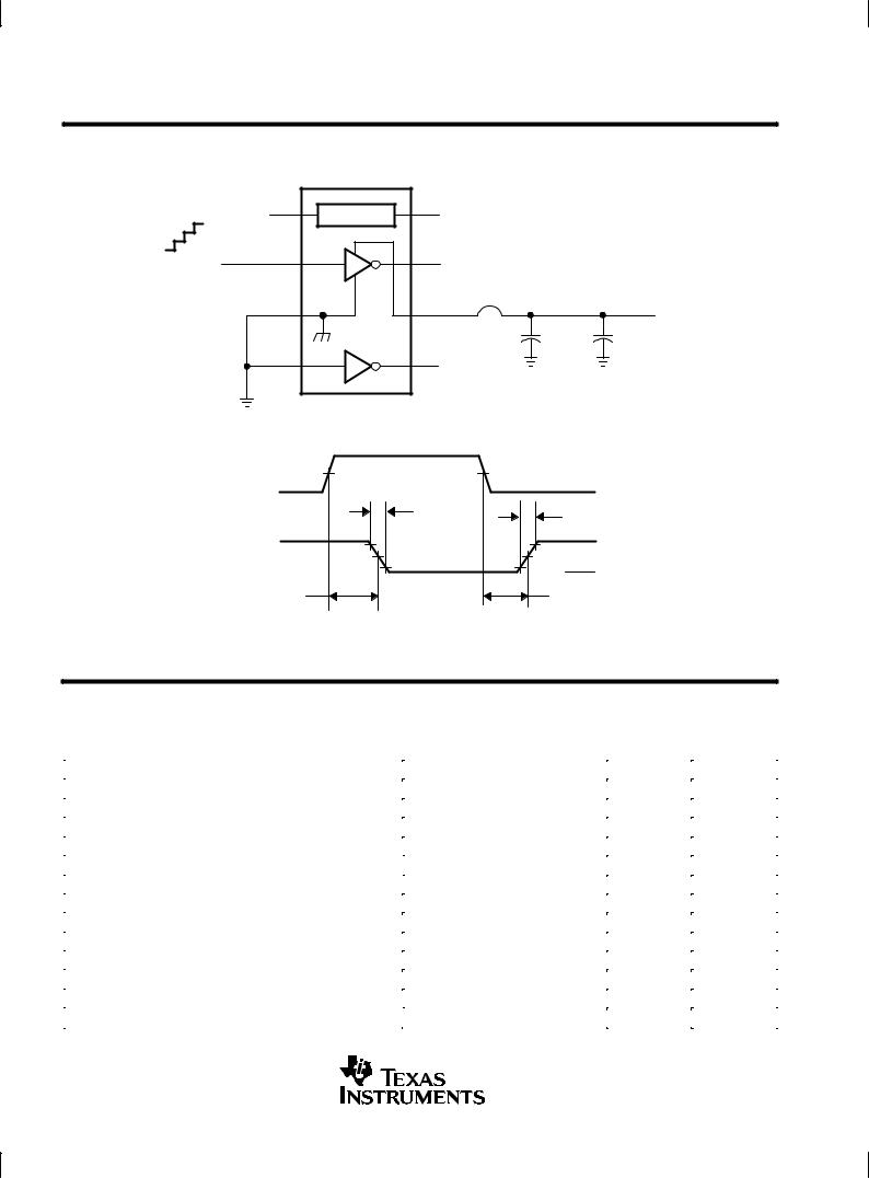
PARAMETER MEASUREMENT INFORMATION
TPS2811 |
|
|
VCC |
|
|
|
|
||
1 |
8 |
|
+ |
|
μF |
4.7 μF |
|||
Regulator |
0.1 |
|||
2 |
7 |
|
Output |
|
Input |
|
|
||
50 Ω |
1 nF |
|
||
3 |
|
|||
6 |
|
|
||
4 |
5 |
|
|
|
NOTE A: Input rise and fall times should be ≤10 ns for accurate measurement of ac parameters.
Figure 1. Test Circuit For Measurement of Switching Characteristics
POST OFFICE BOX 655303 •DALLAS, TEXAS 75265 |
7 |
TPS2811, TPS2812, TPS2813, TPS2814, TPS2815
DUAL HIGH-SPEED MOSFET DRIVERS
SLVS132D ± NOVEMBER 1995 ± REVISED NOVEMBER 1997
PARAMETER MEASUREMENT INFORMATION
|
TPS2811 |
|
|
1 |
8 |
|
|
|
Regulator |
|
|
2 |
7 |
xOUT |
|
0±10 V dc |
|
|
|
|
|
Current |
|
|
|
Loop |
|
3 |
6 |
VCC |
10 V |
|
|
|
|
|
|
|
+ |
|
|
0.1 μF |
4.7 μF |
4 |
5 |
|
|
Figure 2. Shoot-through Current Test Setup
1IN |
50% |
50% |
|
|
|
|
0 V |
|
tf |
tr |
|
|
90% |
90% |
|
1OUT |
50% |
50% |
|
|
10% |
10% |
0 V |
|
tPHL |
tPLH |
|
Figure 3. Typical Timing Diagram (TPS2811)
TYPICAL CHARACTERISTICS
Tables of Characteristics Graphs and Application Information
typical characteristics
PARAMETER |
vs PARAMETER 2 |
FIGURE |
PAGE |
|
|
|
|
|
|
Rise time |
Supply voltage |
4 |
10 |
|
|
|
|
|
|
Fall time |
Supply voltage |
5 |
10 |
|
|
|
|
|
|
Propagation delay time |
Supply voltage |
6, 7 |
10 |
|
|
|
|
|
|
|
Supply voltage |
8 |
11 |
|
|
|
|
|
|
Supply current |
Load capacitance |
9 |
11 |
|
|
|
|
|
|
|
Ambient temperature |
10 |
11 |
|
|
|
|
|
|
Input threshold voltage |
Supply voltage |
11 |
11 |
|
|
|
|
|
|
Regulator output voltage |
Regulator input voltage |
12, 13 |
12 |
|
|
|
|
|
|
Regulator quiescent current |
Regulator input voltage |
14 |
12 |
|
|
|
|
|
|
Peak source current |
Supply voltage |
15 |
12 |
|
|
|
|
|
|
Peak sink current |
Supply voltage |
16 |
13 |
|
|
|
|
|
|
Shoot-through current |
Input voltage, high-to-low |
17 |
13 |
|
|
|
|
|
|
Input voltage, low-to-high |
18 |
13 |
|
|
|
|
|||
|
|
|
|
|
|
|
|
|
|
|
|
|
|
|
8 |
POST OFFICE BOX 655303 •DALLAS, TEXAS 75265 |
TPS2811, TPS2812, TPS2813, TPS2814, TPS2815
DUAL HIGH-SPEED MOSFET DRIVERS
SLVS132D ± NOVEMBER 1995 ± REVISED NOVEMBER 1997
TYPICAL CHARACTERISTICS
Tables of Characteristics Graphs and Application Information (Continued)
general applications
PARAMETER |
|
vs PARAMETER 2 |
FIGURE |
PAGE |
|
|
|
|
|
|
|
Switching test circuits and application information |
|
|
19, 20 |
15 |
|
|
|
|
|
|
|
Voltage of 1OUT vs 2OUT |
Time |
Low-to-high |
21, 23, 25 |
16, 17 |
|
|
|
|
|||
High-to-low |
22, 24, 26 |
16, 17 |
|||
|
|
||||
|
|
|
|
|
circuit for measuring paralleled switching characteristics
PARAMETER |
|
vs PARAMETER 2 |
FIGURE |
PAGE |
|
|
|
|
|
|
|
Switching test circuits and application information |
|
|
27 |
17 |
|
|
|
|
|
|
|
Input voltage vs output voltage |
Time |
Low-to-high |
28, 30 |
18 |
|
|
|
|
|||
High-to-low |
29, 31 |
18 |
|||
|
|
Hex-1 to Hex-4 application information
PARAMETER |
|
vs PARAMETER 2 |
FIGURE |
PAGE |
|
|
|
|
|
Driving test circuit and application information |
|
|
32 |
19 |
|
|
|
|
|
|
|
Hex-1 size |
33 |
20 |
|
|
|
|
|
|
|
Hex-2 size |
36 |
20 |
Drain-source voltage vs drain current |
Time |
|
|
|
Hex-3 size |
39 |
21 |
||
|
|
|
|
|
|
|
Hex-4 size |
41 |
22 |
|
|
|
|
|
|
|
Hex-4 size parallel drive |
45 |
23 |
|
|
|
|
|
|
|
Hex-1 size |
34 |
20 |
|
|
|
|
|
|
|
Hex-2 size |
37 |
21 |
Drain-source voltage vs gate-source voltage at turn-on |
Time |
|
|
|
Hex-3 size |
40 |
21 |
||
|
|
|
|
|
|
|
Hex-4 size |
43 |
22 |
|
|
|
|
|
|
|
Hex-4 size parallel drive |
46 |
23 |
|
|
|
|
|
|
|
Hex-1 size |
35 |
20 |
|
|
|
|
|
|
|
Hex-2 size |
38 |
21 |
Drain-source voltage vs gate-source voltage at turn-off |
Time |
|
|
|
Hex-3 size |
42 |
22 |
||
|
|
|
|
|
|
|
Hex-4 size |
44 |
22 |
|
|
|
|
|
|
|
Hex-4 size parallel drive |
47 |
23 |
synchronous buck regulator application
PARAMETER |
|
vs PARAMETER 2 |
FIGURE |
PAGE |
|
|
|
|
|
3.3-V 3-A Synchronous-Rectified Buck Regulator Circuit |
|
|
48 |
24 |
|
|
|
|
|
Q1 drain voltage vs gate voltage at turn-on |
|
|
49 |
26 |
|
|
|
|
|
Q1 drain voltage vs gate voltage at turn-off |
|
|
50 |
26 |
|
Time |
|
|
|
Q1 drain voltage vs Q2 gate-source voltage |
|
51, 52, 53 |
26, 27 |
|
|
|
|
|
|
Output ripple voltage vs inductor current |
|
3 A |
54 |
27 |
|
|
|
|
|
|
5 A |
55 |
27 |
|
|
|
POST OFFICE BOX 655303 •DALLAS, TEXAS 75265 |
9 |

TPS2811, TPS2812, TPS2813, TPS2814, TPS2815
DUAL HIGH-SPEED MOSFET DRIVERS
SLVS132D ± NOVEMBER 1995 ± REVISED NOVEMBER 1997
|
TYPICAL CHARACTERISTICS |
RISE TIME |
FALL TIME |
vs |
vs |
SUPPLY VOLTAGE |
SUPPLY VOLTAGE |
|
22 |
|
|
|
|
|
|
|
|
|
|
|
|
|
|
|
|
|
CL = 1 nF |
|
|
|
20 |
|
|
|
|
|
|
|
|
|
ns |
18 |
|
|
|
|
|
|
|
|
|
± |
|
|
|
|
|
|
|
TA = 125°C |
|
|
Time |
|
|
|
|
|
|
|
|
||
16 |
|
|
|
|
|
|
TA = 75°C |
|
||
± Rise |
|
|
|
|
|
|
|
|||
|
|
|
|
|
|
|
|
|||
14 |
|
|
|
|
|
|
TA = 25°C |
|
||
r |
|
|
|
|
|
|
|
|
|
|
t |
|
|
|
|
|
|
|
|
|
|
|
|
|
|
|
|
|
° |
TA = ± 50°C |
|
|
|
12 |
|
|
|
|
TA = ±25 C |
|
|
|
|
|
|
|
|
|
|
|
|
|
|
|
|
10 |
|
|
|
|
|
11 |
12 |
13 |
14 |
|
5 |
6 |
7 |
8 |
9 |
10 |
||||
|
|
|
|
VCC ± Supply Voltage ± V |
|
|
||||
|
22 |
|
|
|
|
|
|
|
|
|
|
|
CL = 1 nF |
|
|
|
|
|
|
||
|
20 |
|
|
|
|
|
|
|
|
|
± ns |
18 |
|
|
|
|
|
|
|
|
|
|
|
|
|
|
|
|
TA = 125°C |
|
||
Time |
16 |
|
|
|
|
|
|
TA = 75°C |
|
|
Fall |
|
|
|
|
|
|
|
TA = 25°C |
|
|
± |
14 |
|
|
|
|
|
|
|
|
|
f |
|
|
|
|
|
|
|
|
|
|
t |
|
|
|
|
|
|
|
|
|
|
|
12 |
|
|
|
|
TA = ±25°C |
TA = ± 50°C |
|||
|
|
|
|
|
|
|
|
|
|
|
|
10 |
|
|
|
|
|
11 |
12 |
13 |
14 |
|
5 |
6 |
7 |
8 |
9 |
10 |
||||
|
|
|
|
VCC ± Supply Voltage ± V |
|
|
||||
Figure 4 |
Figure 5 |
PROPAGATION DELAY TIME, HIGH-TO-LOW-LEVEL OUTPUT vs
SUPPLY VOLTAGE
|
|
45 |
|
|
|
|
|
|
|
|
|
|
|
|
CL = 1 nF |
|
|
|
|
|
|
|
|
Delay Time, |
Output ± ns |
40 |
|
|
|
|
|
|
|
|
|
35 |
|
|
|
|
|
|
|
|
|
||
|
|
|
|
|
|
|
|
|
|
||
± Propagation |
-To-Low-Level |
30 |
|
|
|
|
|
TA |
= 125°C |
|
|
|
|
|
|
|
|
|
|||||
25 |
|
|
|
|
|
|
|
|
|
||
PHL High |
|
|
|
|
|
TA = 75°C |
TA = 25°C |
|
|||
t |
|
20 |
|
|
|
|
|
|
|
|
|
|
|
|
|
|
|
|
TA = ± 50°C |
|
|
||
|
|
|
|
|
|
|
|
|
|
||
|
|
15 |
|
|
|
TA = ±25°C |
|
|
|
||
|
|
|
|
|
|
|
|
|
|
|
|
|
|
5 |
6 |
7 |
8 |
9 |
10 |
11 |
12 |
13 |
14 |
|
|
|
|
|
VCC ± Supply Voltage ± V |
|
|
||||
Figure 6
PROPAGATION DELAY TIME, LOW-TO-HIGH-LEVEL OUTPUT vs
SUPPLY VOLTAGE
|
|
45 |
|
|
|
|
|
|
|
|
|
|
|
|
CL = 1 nF |
|
|
|
|
|
|
|
|
|
Output ± ns |
40 |
|
|
|
|
|
|
|
|
|
Delay Time, |
35 |
|
|
|
|
|
|
|
|
|
|
|
|
|
|
TA = 25°C |
|
|
|
|
|||
Propagation |
-High-Level |
30 |
|
|
|
|
TA = 75°C |
|
|
|
|
|
|
|
|
|
|
|
|
|
|||
|
|
|
|
|
|
|
TA=125°C |
|
|||
25 |
|
|
|
|
|
|
|
|
|
||
± |
-To |
|
|
|
|
|
|
|
|
|
|
PLH |
Low |
20 |
|
|
|
|
T |
= ±25°C |
|
|
|
t |
|
|
|
|
A |
|
|
|
|
||
|
|
15 |
|
|
|
|
|
TA = ± 50°C |
|
||
|
|
|
|
|
|
|
|
|
|
|
|
|
|
5 |
6 |
7 |
8 |
9 |
10 |
11 |
12 |
13 |
14 |
|
|
|
|
|
VCC ± Supply Voltage ± V |
|
|
||||
Figure 7
10 |
POST OFFICE BOX 655303 •DALLAS, TEXAS 75265 |
 Loading...