


Texas Instruments TMS370C156AFNT, TMS370C150AFNT, TMS370C758AFNT, TMS370C756ANMT, TMS370C756AFNT Datasheet
...DCMOS/EEPROM/EPROM Technologies on a Single Device
±Mask-ROM Devices for High-Volume Production
±One-Time-Programmable (OTP) EPROM Devices for Low-Volume Production
±Reprogrammable EPROM Devices for Prototyping Purposes
DInternal System Memory Configurations
±On-Chip Program Memory Versions
±ROM: 4K to 48K Bytes
±EPROM: 16K to 48K Bytes
±ROM-less
±Data EEPROM: 256 or 512 Bytes
±Static RAM: 256 to 3.5K Bytes
±External Memory/Peripheral Wait States
±Precoded External Chip-Select Outputs in Microcomputer Mode
DFlexible Operating Features
±Low-Power Modes: STANDBY and HALT
±Commercial, Industrial, and Automotive Temperature Ranges
±Clock Options
±Divide-by-4 (0.5 MHz ± 5 MHz SYSCLK)
±Divide-by-1 (2 MHz ± 5 MHz SYSCLK) Phase-Locked Loop (PLL)
±Supply Voltage (VCC): 5 V ± 10%
DEight-Channel 8-Bit Analog-to-Digital Converter 1 (ADC1)
DTwo 16-Bit General-Purpose Timers
DOn-Chip 24-Bit Watchdog Timer
DTwo Communication Modules
±Serial Communications Interface 1 (SCI1)
±Serial Peripheral Interface (SPI)
DFlexible Interrupt Handling
DTMS370 Series Compatibility
DCMOS/Package /TTL-Compatible I/O Pins
±64-Pin Plastic and Ceramic Shrink Dual-In-Line Packages/44 Bidirectional, 9 Input Pins
±68-Pin Plastic and Ceramic Leaded Chip Carrier Packages/46 Bidirectional,
9 Input Pins
±All Peripheral Function Pins Are Software Configurable for Digital I/O
TMS370Cx5x
8-BIT MICROCONTROLLER
SPNS010F ± DECEMBER 1986 ± REVISED FEBRUARY 1997
FN / FZ PACKAGE
( TOP VIEW )
|
|
|
SS1 |
C2 |
|
C1 |
|
MC |
|
C0 |
B7 |
B6 |
|
B5 B4 |
|
B3 |
|
B2 |
|
B1 |
|
B0 |
|
CSE2 / OCF |
|
CC2 |
SS2 |
CC1 |
|
|
|
|
|
|
|
|
|
|
|
|
||||||||
|
|
|
|
|
|
|
|
|
|
|
|
|
|
|
|
|
|
|
|
|
|
|
|
|
||||||||||||||||||||||||
|
|
|
|
|
|
|
|
|
|
|
|
|
|
|
|
|
|
|
|
|
|
|
|
|
||||||||||||||||||||||||
|
|
|
|
|
|
|
|
|
|
|
|
|
|
|
|
|
|
|
|
|
|
|
|
|
||||||||||||||||||||||||
|
|
|
V |
|
|
|
|
|
|
|
|
|
D0/ |
|
V |
V |
V |
|
|
|
|
|
|
|
|
|
|
|
|
|||||||||||||||||||
|
|
|
|
|
|
|
|
|
|
|
|
|
|
|
|
|
|
|
|
|
|
|
|
|
|
|
|
|
|
|
|
|
|
|
|
|
|
|
|
|
|
|
|
|
|
|
|
|
C3 |
|
9 |
|
8 |
|
7 |
|
6 |
|
5 |
|
4 |
|
3 |
|
2 |
|
1 68 67 66 65 64 63 62 61 |
|
|
|
|
|
|
|
|
|
|
|
|
||||||||||||||||||
|
10 |
|
|
|
|
|
|
|
|
|
|
|
|
|
|
|
|
|
|
|
|
|
|
|
|
|
|
|
|
|
|
|
60 |
|
D1 |
/ |
CSH3 |
|
|
|||||||||
C4 |
|
11 |
|
|
|
|
|
|
|
|
|
|
|
|
|
|
|
|
|
|
|
|
|
|
|
|
|
|
|
|
|
|
|
59 |
|
D2 |
/ |
|
|
|
|
|
|
|
|
|||
|
|
|
|
|
|
|
|
|
|
|
|
|
|
|
|
|
|
|
|
|
|
|
|
|
|
|
|
|
|
|
|
|
CSH2 |
|||||||||||||||
C5 |
|
12 |
|
|
|
|
|
|
|
|
|
|
|
|
|
|
|
|
|
|
|
|
|
|
|
|
|
|
|
|
|
|
|
58 |
|
D3 |
/ SYSCLK |
|||||||||||
C6 |
|
13 |
|
|
|
|
|
|
|
|
|
|
|
|
|
|
|
|
|
|
|
|
|
|
|
|
|
|
|
|
|
|
|
57 |
|
D4 |
/ R / |
|
|
|
|
|
|
|||||
|
|
|
|
|
|
|
|
|
|
|
|
|
|
|
|
|
|
|
|
|
|
|
|
|
|
|
|
|
|
|
|
|
W |
|
|
|
||||||||||||
C7 |
|
14 |
|
|
|
|
|
|
|
|
|
|
|
|
|
|
|
|
|
|
|
|
|
|
|
|
|
|
|
|
|
|
|
56 |
|
D5 |
/ |
|
|
|
|
|
|
|
||||
|
|
|
|
|
|
|
|
|
|
|
|
|
|
|
|
|
|
|
|
|
|
|
|
|
|
|
|
|
|
|
|
|
CSPF |
|||||||||||||||
VCC2 |
|
15 |
|
|
|
|
|
|
|
|
|
|
|
|
|
|
|
|
|
|
|
|
|
|
|
|
|
|
|
|
|
|
|
55 |
|
|
|
|
|
|
|
|
|
|||||
|
|
|
|
|
|
|
|
|
|
|
|
|
|
|
|
|
|
|
|
|
|
|
|
|
|
|
|
|
|
|
|
|
D6/CSH1/EDS |
|||||||||||||||
|
16 |
|
|
|
|
|
|
|
|
|
|
|
|
|
|
|
|
|
|
|
|
|
|
|
|
|
|
|
|
|
|
|
54 |
|
||||||||||||||
VSS2 |
|
|
|
|
|
|
|
|
|
|
|
|
|
|
|
|
|
|
|
|
|
|
|
|
|
|
|
|
|
|
|
|
|
|
|
|
|
|
|
|||||||||
|
|
|
|
|
|
|
|
|
|
|
|
|
|
|
|
|
|
|
|
|
|
|
|
|
|
|
|
|
|
|
|
|
D7/CSE1/WAIT |
|||||||||||||||
|
|
|
|
|
|
|
|
|
|
|
|
|
|
|
|
|
|
|
|
|
|
|
|
|
|
|
|
|
|
|
|
|
|
|
|
|
||||||||||||
A0 |
|
17 |
|
|
|
|
|
|
|
|
|
|
|
|
|
|
|
|
|
|
|
|
|
|
|
|
|
|
|
|
|
|
|
53 |
|
|
RESET |
|
||||||||||
A1 |
|
18 |
|
|
|
|
|
|
|
|
|
|
|
|
|
|
|
|
|
|
|
|
|
|
|
|
|
|
|
|
|
|
|
52 |
|
INT1 |
||||||||||||
A2 |
|
19 |
|
|
|
|
|
|
|
|
|
|
|
|
|
|
|
|
|
|
|
|
|
|
|
|
|
|
|
|
|
|
|
51 |
|
INT2 |
||||||||||||
|
|
|
|
|
|
|
|
|
|
|
|
|
|
|
|
|
|
|
|
|
|
|
|
|
|
|
|
|
|
|
|
|
||||||||||||||||
A3 |
|
20 |
|
|
|
|
|
|
|
|
|
|
|
|
|
|
|
|
|
|
|
|
|
|
|
|
|
|
|
|
|
|
|
50 |
|
INT3 |
||||||||||||
|
|
|
|
|
|
|
|
|
|
|
|
|
|
|
|
|
|
|
|
|
|
|
|
|
|
|
|
|
|
|
|
|
||||||||||||||||
A4 |
|
21 |
|
|
|
|
|
|
|
|
|
|
|
|
|
|
|
|
|
|
|
|
|
|
|
|
|
|
|
|
|
|
|
49 |
|
SPISOMI |
||||||||||||
|
|
|
|
|
|
|
|
|
|
|
|
|
|
|
|
|
|
|
|
|
|
|
|
|
|
|
|
|
|
|
|
|
||||||||||||||||
A5 |
|
22 |
|
|
|
|
|
|
|
|
|
|
|
|
|
|
|
|
|
|
|
|
|
|
|
|
|
|
|
|
|
|
|
48 |
|
SPISIMO |
||||||||||||
|
|
|
|
|
|
|
|
|
|
|
|
|
|
|
|
|
|
|
|
|
|
|
|
|
|
|
|
|
|
|
|
|
||||||||||||||||
A6 |
|
23 |
|
|
|
|
|
|
|
|
|
|
|
|
|
|
|
|
|
|
|
|
|
|
|
|
|
|
|
|
|
|
|
47 |
|
SPICLK |
||||||||||||
|
|
|
|
|
|
|
|
|
|
|
|
|
|
|
|
|
|
|
|
|
|
|
|
|
|
|
|
|
|
|
|
|
||||||||||||||||
A7 |
|
24 |
|
|
|
|
|
|
|
|
|
|
|
|
|
|
|
|
|
|
|
|
|
|
|
|
|
|
|
|
|
|
|
46 |
|
T1IC/CR |
||||||||||||
|
|
|
|
|
|
|
|
|
|
|
|
|
|
|
|
|
|
|
|
|
|
|
|
|
|
|
|
|
|
|
|
|
||||||||||||||||
T2AEVT |
|
25 |
|
|
|
|
|
|
|
|
|
|
|
|
|
|
|
|
|
|
|
|
|
|
|
|
|
|
|
|
|
|
|
45 |
|
T1PWM |
||||||||||||
|
|
|
|
|
|
|
|
|
|
|
|
|
|
|
|
|
|
|
|
|
|
|
|
|
|
|
|
|
|
|
|
|
||||||||||||||||
T2AIC2/PWM |
|
26 |
|
|
|
|
|
|
|
|
|
|
|
|
|
|
|
|
|
|
|
|
|
|
|
|
|
|
|
|
|
|
|
44 |
|
T1EVT |
||||||||||||
|
|
|
|
|
|
|
|
|
|
|
|
|
|
|
|
|
|
|
|
|
|
|
|
|
|
|
|
|
|
|
|
|
||||||||||||||||
|
|
|
27 28 29 30 31 32 33 34 35 36 37 38 39 40 41 42 43 |
|
|
|
|
|
|
|
|
|
|
|
|
|||||||||||||||||||||||||||||||||
|
|
|
|
|
|
|
|
|
|
|
|
|
|
|
|
|
|
|
|
|
|
|
|
|
|
|
|
|
|
|
|
|
|
|
|
|
|
|
|
|
|
|
|
|
|
|
|
|
|
|
|
T2AIC1/CR |
SCICLK |
|
SCIRXD |
|
SCITXD |
|
XTAL2/CLKIN |
XTAL1 |
V |
|
V |
|
V |
|
AN0 |
|
AN1 |
|
AN2 |
|
AN3 |
|
AN4 |
|
AN5 |
AN6 |
AN7 |
|
|
|
|
|
|
|
|
|
|
|
|
||||||
|
|
|
|
|
|
|
|
|
|
|
|
|
|
|
CC1 |
|
CC3 |
|
SS3 |
|
|
|
|
|
|
|
|
|
|
|
|
|
|
|
|
|
|
|
|
|
|
|
|
|
|
|
|
|
JN / NM PACKAGE
( TOP VIEW )
B5 |
|
1 |
64 |
|
|
B4 |
|||||||||||
|
|
|
|||||||||||||||
B6 |
|
2 |
63 |
|
|
B3 |
|||||||||||
|
|
||||||||||||||||
B7 |
|
3 |
62 |
|
|
B2 |
|||||||||||
|
|
||||||||||||||||
C0 |
|
4 |
61 |
|
|
B1 |
|||||||||||
|
|
||||||||||||||||
MC |
|
5 |
60 |
|
|
B0 |
|||||||||||
|
|
||||||||||||||||
C1 |
|
|
|
|
|
D0 / |
|
|
|
|
/ |
|
|
|
|
|
|
|
6 |
59 |
|
CSE2 |
OCF |
||||||||||||
C2 |
|
7 |
58 |
|
|
VSS1 |
|||||||||||
VSS1 |
|
8 |
57 |
|
|
VCC1 |
|||||||||||
|
|
||||||||||||||||
C3 |
|
|
|
|
|
D1 / |
|
|
|
|
|
|
|
|
|||
|
9 |
56 |
|
CSH3 |
|||||||||||||
C4 |
|
10 |
55 |
|
|
D3 / SYSCLK |
|||||||||||
C5 |
|
|
|
|
|
D4 / R / |
|
|
|
|
|
||||||
|
11 |
54 |
|
W |
|||||||||||||
C6 |
|
12 |
53 |
|
|
D6 / |
CSH1 |
/ |
EDS |
|
|
||||||
C7 |
|
13 |
52 |
|
|
D7 / |
CSE1 |
/ |
WAIT |
|
|||||||
AN0 |
|
14 |
51 |
|
|
RESET |
|
||||||||||
A0 |
|
15 |
50 |
|
|
INT1 |
|||||||||||
A1 |
|
16 |
49 |
|
|
INT2 |
|||||||||||
|
|
||||||||||||||||
A2 |
|
17 |
48 |
|
|
INT3 |
|||||||||||
|
|
||||||||||||||||
A3 |
|
18 |
47 |
|
|
SPISOMI |
|||||||||||
|
|
||||||||||||||||
A4 |
|
19 |
46 |
|
|
SPISIMO |
|||||||||||
|
|
||||||||||||||||
A5 |
|
20 |
45 |
|
|
SPICLK |
|||||||||||
|
|
||||||||||||||||
A6 |
|
21 |
44 |
|
|
T1IC / CR |
|||||||||||
|
|
||||||||||||||||
A7 |
|
22 |
43 |
|
|
T1PWM |
|||||||||||
|
|
||||||||||||||||
T2AEVT |
|
23 |
42 |
|
|
AN7 |
|||||||||||
|
|
||||||||||||||||
T2AIC2 / PWM |
|
24 |
41 |
|
|
T1EVT |
|||||||||||
|
|
||||||||||||||||
T2AIC1 / CR |
|
25 |
40 |
|
|
VSS1 |
|||||||||||
|
|
||||||||||||||||
SCICLK |
|
26 |
39 |
|
|
AN6 |
|||||||||||
|
|
||||||||||||||||
SCIRXD |
|
27 |
38 |
|
|
AN5 |
|||||||||||
|
|
||||||||||||||||
SCITXD |
|
28 |
37 |
|
|
AN4 |
|||||||||||
|
|
||||||||||||||||
XTAL2 / CLKIN |
|
29 |
36 |
|
|
AN3 |
|||||||||||
|
|
||||||||||||||||
XTAL1 |
|
30 |
35 |
|
|
AN2 |
|||||||||||
|
|
||||||||||||||||
VCC1 |
|
31 |
34 |
|
|
AN1 |
|||||||||||
|
|
||||||||||||||||
VCC3 |
|
32 |
33 |
|
|
VSS3 |
|||||||||||
|
|
||||||||||||||||
|
|
|
|
|
|
|
|
|
|
|
|
|
|
|
|
|
|
DWorkstation/PC-Based Development System
±C Compiler and C Source Debugger
±Real-Time In-Circuit Emulation
±Extensive Breakpoint/Trace Capability
±Software Performance Analysis
±Multi-Window User Interface
±Microcontroller Programmer
Please be aware that an important notice concerning availability, standard warranty, and use in critical applications of Texas Instruments semiconductor products and disclaimers thereto appears at the end of this data sheet.
PRODUCTION DATA information is current as of publication date. Products conform to specifications per the terms of Texas Instruments standard warranty. Production processing does not necessarily include testing of all parameters.
POST OFFICE BOX 1443 •HOUSTON, TEXAS 77251±1443
Copyright 1997, Texas Instruments Incorporated
1

TMS370Cx5x
8-BIT MICROCONTROLLER
SPNS010F ± DECEMBER 1986 ± REVISED FEBRUARY 1997
|
|
|
|
|
|
|
Pin Descriptions |
||
|
|
|
|
|
|
|
|
|
|
|
|
|
PIN |
|
|
|
|
|
|
|
|
|
|
|
|
|
|
|
|
|
NAME |
ALTERNATE |
SDIP |
LCC |
I/O² |
|
DESCRIPTION³ |
||
|
FUNCTION |
(64) |
(68) |
|
|
|
|
||
|
|
|
|
|
|
|
|||
|
|
|
|
|
|
|
|
|
|
|
A0 |
DATA0 |
15 |
17 |
|
|
|
|
|
|
A1 |
DATA1 |
16 |
18 |
|
|
|
|
|
|
A2 |
DATA2 |
17 |
19 |
|
Single-chip mode: Port A is a general-purpose bidirectional I/O port. |
|||
|
A3 |
DATA3 |
18 |
20 |
|
||||
|
I / O |
Expansion mode: Port A can be individually programmed as the external |
|||||||
|
A4 |
DATA4 |
19 |
21 |
|||||
|
|
bidirectional data bus (DATA0 ± DATA7). |
|||||||
|
A5 |
DATA5 |
20 |
22 |
|
||||
|
|
|
|
|
|||||
|
A6 |
DATA6 |
21 |
23 |
|
|
|
|
|
|
A7 |
DATA7 |
22 |
24 |
|
|
|
|
|
|
|
|
|
|
|
|
|
|
|
|
B0 |
ADDR0 |
60 |
65 |
|
|
|
|
|
|
B1 |
ADDR1 |
61 |
66 |
|
|
|
|
|
|
B2 |
ADDR2 |
62 |
67 |
|
Single-chip mode: Port B is a general-purpose bidirectional I/O port. |
|||
|
B3 |
ADDR3 |
63 |
68 |
|
||||
|
I / O |
Expansion mode: Port B can be individually programmed as the low-order address |
|||||||
|
B4 |
ADDR4 |
64 |
1 |
|||||
|
|
output bus (ADDR0 ± ADDR7). |
|||||||
|
B5 |
ADDR5 |
1 |
2 |
|
||||
|
|
|
|
|
|||||
|
B6 |
ADDR6 |
2 |
3 |
|
|
|
|
|
|
B7 |
ADDR7 |
3 |
4 |
|
|
|
|
|
|
|
|
|
|
|
|
|
|
|
|
C0 |
ADDR8 |
4 |
5 |
|
|
|
|
|
|
C1 |
ADDR9 |
6 |
7 |
|
|
|
|
|
|
C2 |
ADDR10 |
7 |
8 |
|
Single-chip mode: Port C is a general-purpose bidirectional I/O port. |
|||
|
C3 |
ADDR11 |
9 |
10 |
|
||||
|
I / O |
Expansion mode: Port C can be individually programmed as the high-order address |
|||||||
|
C4 |
ADDR12 |
10 |
11 |
|||||
|
|
output bus (ADDR8 ± ADDR15). |
|||||||
|
C5 |
ADDR13 |
11 |
12 |
|
||||
|
|
|
|
|
|||||
|
C6 |
ADDR14 |
12 |
13 |
|
|
|
|
|
|
C7 |
ADDR15 |
13 |
14 |
|
|
|
|
|
|
|
|
|
|
|
|
|
|
|
|
INT1 |
NMI |
50 |
52 |
I |
External (nonmaskable or maskable) interrupt/general-purpose input pin |
|||
|
INT2 |
Ð |
49 |
51 |
I / O |
External maskable interrupt input/general-purpose bidirectional pin |
|||
|
INT3 |
Ð |
48 |
50 |
I / O |
External maskable interrupt input/general-purpose bidirectional pin |
|||
|
|
|
|
|
|
|
|
|
|
|
AN0 |
E0 |
14 |
36 |
|
|
|
|
|
|
AN1 |
E1 |
34 |
37 |
|
|
|
|
|
|
AN2 |
E2 |
35 |
38 |
|
ADC1 analog input (AN0 ± AN7) or positive reference pins (AN1 ± AN7) |
|||
|
AN3 |
E3 |
36 |
39 |
|
||||
|
I |
Port E can be individually programmed as general-purpose input pins if not used |
|||||||
|
AN4 |
E4 |
37 |
40 |
|||||
|
|
as ADC1 analog input or positive reference input. |
|||||||
|
AN5 |
E5 |
38 |
41 |
|
||||
|
|
|
|
|
|||||
|
AN6 |
E6 |
39 |
42 |
|
|
|
|
|
|
AN7 |
E7 |
42 |
43 |
|
|
|
|
|
|
|
|
|
|
|
|
|
|
|
|
VCC3 |
|
32 |
34 |
|
ADC1 positive-supply voltage and optional positive-reference input pin |
|||
|
VSS3 |
|
33 |
35 |
|
ADC1 ground reference pin |
|||
|
|
|
|
|
|
|
System reset bidirectional pin. |
|
as an input, initializes the microcontroller; |
|
|
|
|
|
|
|
RESET, |
||
|
RESET |
|
|
51 |
53 |
I / O |
as open-drain output, RESET indicates an internal failure was detected by the |
||
|
|
|
|
|
|
|
watchdog or oscillator fault circuit. |
||
|
|
|
|
|
|
|
|
|
|
|
|
|
|
|
|
|
Mode control (MC) pin. MC enables EEPROM write-protection override (WPO) |
||
|
MC |
|
5 |
6 |
I |
mode, also EPROM VPP. |
|||
|
|
|
|
|
|
|
|||
|
XTAL2/CLKIN |
|
29 |
31 |
I |
Internal oscillator crystal input / external clock source input |
|||
|
XTAL1 |
|
30 |
32 |
O |
Internal oscillator output for crystal |
|||
|
|
|
|
|
|
|
|
|
|
|
VCC1 |
|
31, 57 |
33, |
|
Positive supply voltage |
|||
|
|
61 |
|
||||||
|
|
|
|
|
|
|
|
|
|
|
|
|
|
|
|
|
|||
|
VCC2 |
|
Ð |
15,63 |
|
Positive supply voltage |
|||
² I = input, O = output
³ Ports A, B, C, and D can be configured only as general-purpose I/O pins. Also, port D3 can be configured as SYSCLK.
2 |
POST OFFICE BOX 1443 •HOUSTON, TEXAS 77251±1443 |
|
|
|
|
|
|
TMS370Cx5x |
|
|
|
|
|
|
8-BIT MICROCONTROLLER |
|
|
|
|
|
|
SPNS010F ± DECEMBER 1986 ± REVISED FEBRUARY 1997 |
|
|
|
|
Pin Descriptions (Continued) |
||
|
PIN |
|
|
|
|
|
NAME |
ALTERNATE |
SDIP |
LCC |
I/O² |
DESCRIPTION³ |
|
FUNCTION |
(64) |
(68) |
|
|
||
|
|
|
||||
VSS1 |
|
|
8, |
9 |
|
Ground reference for digital logic |
|
|
58,40 |
|
|||
|
|
|
|
|
|
|
VSS2 |
|
|
Ð |
16,62 |
|
Ground reference for digital I / O logic |
|
FUNCTION |
|
|
|
Single-chip mode: Port D is a general-purpose bidirectional I / O port. Each of |
|
|
|
|
|
the port D pins can be individually configured as a general-purpose I / O pin, |
||
|
|
|
|
|
|
|
|
|
|
|
|
|
primary memory control signal (function A), or secondary memory control |
|
A |
B |
|
|
|
signal (function B). All chip selects are independent and can be used for |
|
|
|
|
memory bank switching. Refer to Table 1 for function A memory accesses. |
||
|
|
|
|
|
|
|
D0 |
CSE2 |
OCF |
59 |
64 |
|
I / O pin A: Chip select eighth output 2 goes low during memory accesses |
|
I / O pin B: Opcode fetch goes low during the opcode fetch memory cycle. |
|||||
|
|
|
|
|
|
|
D1 |
CSH3 |
Ð |
56 |
60 |
|
I / O pin A: Chip select half output 3 goes low during memory accesses. |
|
I / O pin B: Reserved |
|||||
|
|
|
|
|
|
|
D2 |
CSH2 |
Ð |
Ð |
59 |
|
I / O pin A: Chip select half output 2 goes low during memory accesses. |
|
I / O pin B: Reserved |
|||||
|
|
|
|
|
|
|
D3 |
SYSCLK |
SYSCLK |
55 |
58 |
|
I / O pin A, B: Internal clock signal is 1 / 1 (PLL) or 1 / 4 XTAL2/ CLKIN frequency. |
D4 |
R / W |
R / W |
54 |
57 |
I / O |
I / O pin A, B: Read / write output pin |
|
|
|
|
|
|
|
|
|
|
|
|
|
I / O pin A: Chip select peripheral output for peripheral file goes low during |
D5 |
CSPF |
Ð |
Ð |
56 |
|
memory accesses. |
|
|
|
|
|
|
I / O pin B: Reserved |
|
|
|
|
|
|
I / O pin A: Chip select half output 1 goes low during memory accesses. |
D6 |
CSH1 |
EDS |
53 |
55 |
|
I / O pin B: External data strobe output goes low during memory accesses from |
|
|
|
|
|
|
external memory and has the same timings as the five chip selects. |
D7 |
CSE1 |
WAIT |
52 |
54 |
|
I / O pin A: Chip select eighth output goes low during memory accesses. |
|
I / O pin B: Wait input pin extends bus signals. |
|||||
|
|
|
|
|
|
|
SCITXD |
SCIIO1 |
28 |
30 |
|
|
SCI transmit data output pin / general-purpose bidirectional pin (see Note 1) |
|
SCIRXD |
SCIIO2 |
27 |
29 |
I / O |
|
SCI receive data input pin / general-purpose bidirectional pin |
|
SCICLK |
SCIIO3 |
26 |
28 |
|
|
SCI bidirectional serial clock pin / general-purpose bidirectional pin |
|
|
|
|
|
|
|
|
|
|
|
|
|
|
|
Timer1 input capture / counter reset input pin / general-purpose bidirectional |
|
T1IC / CR |
T1IO1 |
44 |
46 |
|
|
pin |
|
T1PWM |
T1IO2 |
43 |
45 |
I / O |
|
Timer1 pulse-width-modulation (PWM) output pin / general-purpose |
|
T1EVT |
T1IO3 |
41 |
44 |
|
|
bidirectional pin |
|
|
|
|
|
|
|
Timer1 external event input pin / general-purpose bidirectional pin |
|
|
|
|
|
|
|
|
|
T2AIC1/ CR |
T2AIO1 |
25 |
27 |
|
|
Timer2A input capture 1 / counter reset input pin / general-purpose bidirectional |
|
|
|
pin |
|
||||
T2AIC2/ PWM |
T2AIO2 |
24 |
26 |
I / O |
|
|
|
|
Timer2A input capture 2 / PWM output pin / general-purpose bidirectional pin |
|
|||||
T2AEVT |
T2AIO3 |
23 |
25 |
|
|
|
|
|
|
Timer2A external event input pin / general-purpose bidirectional pin |
|
||||
|
|
|
|
|
|
|
|
|
|
|
|
|
|
|
|
SPISOMI |
SPIIO1 |
47 |
49 |
|
|
SPI slave output pin, master input pin / general-purpose bidirectional pin |
|
SPISIMO |
SPIIO2 |
46 |
48 |
I / O |
|
SPI slave input pin, master output pin / general-purpose bidirectional pin |
|
SPICLK |
SPIIO3 |
45 |
47 |
|
|
SPI bidirectional serial clock pin / general-purpose bidirectional pin |
|
|
|
|
|
|
|
|
|
² I = input, O = output
³ Ports A, B, C, and D can be configured only as general-purpose I/O pins. Port D3 also can be configured as SYSCLK. NOTE 1: The three-pin configuration SCI is referred to as SCI1.
Table 1. Function A: Memory Accesses Locations for `x5x Devices
|
|
|
|
FUNCTION A |
`X50, `X52, `X53, AND `X56 |
`X58 |
`X59 |
|
||
|
|
|
|
|
|
|
|
|
|
|
|
|
|
|
|
2000h |
± 3FFFh (8K bytes) |
A000h ± BFFFh (8K bytes) |
E000h ± EFFFh (4K bytes) |
|
|
|
CSEx |
|
|
|
|
|||||
|
|
|
|
|
|
|
|
|
|
|
|
|
|
|
|
8000h |
± FFFFh (32K bytes) |
C000h ± FFFFh (16K bytes) |
F000h ± FFFFh |
(4K bytes) |
|
|
CSHx |
|
|
|
||||||
|
|
|
|
|
|
|
|
|
||
|
|
|
|
|
10C0h ± 10FFh (64 bytes) |
10C0h ± 10FFh (64 bytes) |
10C0h ± 10FFh |
(64 bytes) |
|
|
|
CSPF |
|
|
|||||||
|
|
|
|
|
|
|
|
|
|
|
|
|
|
|
|
|
|
|
|
|
|
POST OFFICE BOX 1443 •HOUSTON, TEXAS 77251±1443 |
3 |
TMS370Cx5x
8-BIT MICROCONTROLLER
SPNS010F ± DECEMBER 1986 ± REVISED FEBRUARY 1997
functional block diagram
|
|
|
|
|
|
|
E0 ± E7 |
|
|
|
|
|
|
|
|
|
or |
|
|
INT1 |
INT2 |
INT3 XTAL1 XTAL2/ |
MC |
RESET |
AN0 ± AN7 |
|
|||
|
|
|
|
CLKIN |
|
|
|
|
|
|
|
|
Clock Options: |
|
|
Analog-to-Digital |
VCC3 |
||
|
Interrupts |
|
System Control |
|
|||||
|
|
Divide-by-4 or |
|
||||||
|
|
Converter 1 |
|
||||||
|
|
|
Divide-by-1(PLL) |
|
|
|
|||
|
|
|
|
|
|
VSS3 |
|||
|
|
|
|
|
|
|
|
||
|
|
|
|
|
|
|
Serial |
SPISOMI |
|
|
|
|
|
|
RAM |
|
Peripheral |
SPISIMO |
|
|
|
|
|
|
|
Interface |
SPICLK |
||
|
CPU |
|
256, 512, 1K, 1.5K, or |
||||||
|
|
|
|
3.5K Bytes |
Serial |
SCIRXD |
|||
|
|
|
|
|
|
|
|||
|
Program Memory |
Data EEPROM |
Communications |
SCITXD |
|||||
|
Interface 1 |
SCICLK |
|||||||
ROM: 4K, 8K, 12K, 16K, |
|||||||||
0, 256, or 512 Bytes |
|
||||||||
|
32K, or 48K Bytes |
|
T2AIC1 / CR |
||||||
|
|
|
|
|
|||||
EPROM: 16K, 32K, or |
|
|
|
|
|||||
|
|
|
Timer 2A |
T2AEVT |
|||||
|
48K Bytes |
|
|
|
|||||
|
|
|
|
|
T2AIC2 / PWM |
||||
|
|
|
|
|
|
|
|
||
|
|
|
|
|
|
|
Timer 1 |
T1IC / CR |
|
|
|
|
|
|
|
|
T1EVT |
||
|
|
|
Memory Expansion |
|
|
|
T1PWM |
||
|
|
|
AddressLSbyte |
AddressMSbyte |
|
|
Watchdog |
|
|
|
Data |
|
|
Control |
|
|
|||
Port A |
|
Port B |
Port C |
|
Port D² |
|
V |
||
|
|
|
|
|
|
|
|
CC1 |
|
|
|
|
|
|
|
|
|
VSS1 |
|
|
8 |
|
8 |
8 |
|
8/6 |
|
|
|
|
|
|
|
|
|
VSS2 |
VCC2 |
|
|
² For the 64-pin devices, there are only six pins for port D.
description
The TMS370Cx5x family of single-chip 8-bit microcontrollers provides cost-effective real-time system control through integration of advanced peripheral function modules and various on-chip memory configurations. The TMS370Cx5x family presently consists of twenty-one devices which are grouped into seven main sub-families: the TMS370Cx50, TMS370Cx52, TMS370Cx53, TMS370Cx56, TMS370Cx58, TMS370Cx59, and SE370C75x.
The TMS370Cx5x family of devices is implemented using high-performance silicon-gate CMOS EPROM and EEPROM technologies. The low-operating power, wide-operating temperature range, and noise immunity of CMOS technology, coupled with the high performance and extensive on-chip peripheral functions, make the TMS370Cx5x devices attractive in system designs for automotive electronics, industrial motor control, computer peripheral control, telecommunications, and consumer application. Table 2 provides a memory configuration overview of the TMS370Cx5x devices.
4 |
POST OFFICE BOX 1443 •HOUSTON, TEXAS 77251±1443 |
TMS370Cx5x
8-BIT MICROCONTROLLER
SPNS010F ± DECEMBER 1986 ± REVISED FEBRUARY 1997
description (continued)
Table 2. Memory Configurations
|
PROGRAM |
OFF-CHIP |
DATA MEMORY |
OPERATING |
PACKAGES |
||||
|
MEMORY |
||||||||
DEVICE |
MEMORY |
(BYTES) |
MODES |
68 PIN PLCC/CLCC, OR |
|||||
(BYTES) |
|||||||||
|
EXP. (BYTES) |
|
|
|
|
64 PIN PSDIP/CSDIP |
|||
|
|
|
|
|
|
|
|||
|
ROM |
EPROM |
RAM |
EEPROM |
C² |
P² |
|||
|
|
|
|||||||
|
TMS370Cx50: TMS370C050, TMS370C150, TMS370C250, AND TMS370C350 |
|
||||||
TMS370C050A |
4K |
Ð |
112K |
256 |
256 |
√ |
√ |
FN ± PLCC / NM ±PSDIP |
TMS370C150A |
Ð |
Ð |
56K |
256 |
Ð |
Ð |
√ |
FN ± PLCC |
TMS370C250A |
Ð |
Ð |
56K |
256 |
256 |
Ð |
√ |
FN ± PLCC |
TMS370C350A |
4K |
Ð |
112K |
256 |
Ð |
√ |
√ |
FN ± PLCC / NM ±PSDIP |
|
TMS370Cx52: TMS370C052, TMS370C352, AND TMS370C452 |
|
||||||
TMS370C052A |
8K |
|
Ð |
112K |
256 |
256 |
√ |
|
√ |
FN ± PLCC / NM ±PSDIP |
|
|
|
|
|
|
|
|
|
|
|
|
|
TMS370C352A |
8K |
|
Ð |
112K |
256 |
Ð |
√ |
|
√ |
FN ± PLCC / NM ±PSDIP |
|
|
|
|
|
|
|
|
|
|
|
|
|
TMS370C452A³ |
8K |
|
Ð |
112K |
256 |
256 |
√ |
|
√ |
FN ± PLCC |
|
|
|
|
|
TMS370Cx53: TMS370C353 |
|
|
|
|
|
||
|
|
|
|
|
|
|
|
|
|
||
TMS370C353A |
12K |
|
Ð |
112K |
1.5K |
Ð |
√ |
|
√ |
FN ± PLCC |
|
|
|
|
|
|
|
|
|
|
|
||
TMS370Cx56: TMS370C056, TMS370C156, TMS370C256, TMS370C356, TMS370C456, AND TMS370C756 |
|||||||||||
|
|
|
|
|
|
|
|
|
|||
TMS370C056A |
16K |
|
Ð |
112K |
512 |
512 |
√ |
|
√ |
FN ± PLCC / NM ±PSDIP |
|
|
|
|
|
|
|
|
|
|
|
|
|
TMS370C156A |
Ð |
|
Ð |
56K |
512 |
Ð |
Ð |
|
√ |
FN ± PLCC |
|
|
|
|
|
|
|
|
|
|
|
|
|
TMS370C256A |
Ð |
|
Ð |
56K |
512 |
512 |
Ð |
|
√ |
FN ± PLCC |
|
|
|
|
|
|
|
|
|
|
|
|
|
TMS370C356A |
16K |
|
Ð |
112K |
512 |
Ð |
√ |
|
√ |
FN ± PLCC / NM ±PSDIP |
|
|
|
|
|
|
|
|
|
|
|
|
|
TMS370C456A³ |
16K |
|
Ð |
112K |
512 |
512 |
√ |
|
√ |
FN ± PLCC |
|
TMS370C756A |
Ð |
|
16K |
112K |
512 |
512 |
√ |
|
√ |
FN ± PLCC / NM ±PSDIP |
|
|
|
|
|
|
|
|
|
|
|
||
|
TMS370Cx58: TMS370C058, TMS370C358, AND TMS370C758 |
|
|
||||||||
|
|
|
|
|
|
|
|
|
|||
TMS370C058A |
32K |
|
Ð |
64K |
1K |
256 |
√ |
|
√ |
FN ± PLCC / NM ±PSDIP |
|
|
|
|
|
|
|
|
|
|
|
|
|
TMS370C358A |
32K |
|
Ð |
64K |
1K |
Ð |
√ |
|
√ |
FN ± PLCC / NM ±PSDIP |
|
|
|
|
|
|
|
|
|
|
|
|
|
TMS370C758A, |
Ð |
|
32K |
64K |
1K |
256 |
√ |
|
√ |
FN ± PLCC / NM ±PSDIP |
|
TMS370C758B |
|
|
|
||||||||
|
|
|
|
|
|
|
|
|
|
|
|
|
|
|
|
|
|
|
|
|
|
|
|
|
|
|
TMS370Cx59: TMS370C059 AND TMS370C759 |
|
|
|
|||||
|
|
|
|
|
|
|
|
|
|||
TMS370C059A§ |
48K |
|
Ð |
20K |
3.5K |
256 |
√ |
|
√ |
FN ± PLCC |
|
TMS370C759A§ |
Ð |
|
48K |
20K |
3.5K |
256 |
√ |
|
√ |
FN ± PLCC |
|
|
|
EPROM DEVICE: SE370C756, SE370C758, and SE370C759 |
|
|
|
||||||
|
|
|
|
|
|
|
|
|
|
||
SE370C756A¶ |
Ð |
|
16K |
112K |
512 |
512 |
√ |
|
√ |
FZ ± CLCC / JN ±CSDIP |
|
SE370C758A¶ , |
Ð |
|
32K |
64K |
1K |
256 |
√ |
|
√ |
FZ ± CLCC / JN ±CSDIP |
|
SE370C758B¶ |
|
|
|
||||||||
|
|
|
|
|
|
|
|
|
|
|
|
SE370C759A§¶ |
Ð |
|
48K |
20K |
3.5K |
256 |
√ |
√ |
FZ ± CLCC |
||
² C ± Microcomputer modeP ± Microprocessor mode
³ TMS370C45x support ROM memory security. Refer to the program ROM section. § Only operate up to 3 MHz SYSCLK
¶ System evaluators and development tools are for use only in a prototype environment, and their reliability has not been characterized.
POST OFFICE BOX 1443 •HOUSTON, TEXAS 77251±1443 |
5 |

TMS370Cx5x
8-BIT MICROCONTROLLER
SPNS010F ± DECEMBER 1986 ± REVISED FEBRUARY 1997
description (continued)
The suffix letter (A or B) appended to the device names shown in the device column of Table 2 indicates the configuration of the device. ROM or an EPROM devices have different configurations as indicated in Table 3. ROM devices with the suffix letter A are configured through a programmable contact during manufacture.
Table 3. Suffix Letter Configuration
DEVICE² |
WATCHDOG TIMER |
CLOCK |
LOW-POWER MODE |
EPROM A |
Standard |
Divide-by-4 (Standard oscillator) |
Enabled |
|
|
|
|
EPROM B |
Hard |
Divide-by-1 (PLL) |
Enabled |
|
|
|
|
|
Standard |
|
|
ROM A |
|
Divide-by-4 or Divide-by-1 (PLL) |
Enabled or disabled |
Hard |
|||
|
|
|
|
|
Simple |
|
|
|
|
|
|
ROM-less A |
Standard |
Divide-by-4 |
Enabled |
² Refer to the ªdevice numbering conventionsº section for device nomenclature and the ªdevice part numbersº section for ordering.
Unless otherwise noted, the terms TMS370Cx50, TMS370Cx52, TMS370Cx53, TMS370Cx56, TMS370Cx58, TMS370Cx59, and SE370C75x refer to the individual devices listed in Table 2 and described in this data sheet. All TMS370Cx5x devices contain the following on-chip peripheral modules:
DEight-channel, 8-bit analog-to-digital converter 1 (ADC1)
DSerial communications interface 1 (SCI1)
DSerial peripheral interface (SPI)
DOne 24-bit general-purpose watchdog timer
DTwo 16-bit general-purpose timers (one with an 8-bit prescaler)
TMS370C756, TMS370C758, and TMS370C759 are one-time programmable (OTP) devices that are available in plastic packages. This microcomputer is effective to use for immediate production updates for other members of the TMS370Cx5x family or for low-volume production runs when the mask charge or cycle time for low-cost mask ROM devices is not practical.
The SE370C756, SE370C758, and SE370C759 have windowed ceramic packages to allow reprogramming of the program EPROM memory during the development/prototyping phase of design. The SE370C75x devices allow quick updates to breadboards and prototype systems while iterating initial designs.
The TMS370Cx5x family provides two low-power modes (STANDBY and HALT) for applications where low-power consumption is critical. Both modes stop all central processing unit (CPU) activity (that is, no instructions are executed). In the STANDBY mode, the internal oscillator and the general-purpose timer remain active. In the HALT mode, all device activity is stopped. The device retains all RAM data and peripheral configuration bits throughout both low-power modes.
The TMS370Cx5x features advanced register-to-register architecture that allows direct arithmetic and logical operations without requiring an accumulator (for example, ADD R24, R47; add the contents of register 24 to the contents of register 47 and store the result in register 47). The TMS370Cx5x family is fully instruction-set-compatible, allowing easy transition between members of the TMS370 8-bit microcontroller family.
The SPI and the two operational modes of the SCI1 give three methods of serial communications. The SCI1 allows standard RS-232-C communications interface between other common data transmission equipment, while the SPI gives high-speed communications between simpler shift-register type devices, such as display drivers, ADC1 converter, phase-locked loop (PLL), I/O expansion, or other microcontrollers in the system.
6 |
POST OFFICE BOX 1443 •HOUSTON, TEXAS 77251±1443 |

TMS370Cx5x
8-BIT MICROCONTROLLER
SPNS010F ± DECEMBER 1986 ± REVISED FEBRUARY 1997
description (continued)
For large memory applications, the TMS370Cx5x family provides an external bus with non-multiplexed address and data. Precoded memory chip-select outputs can be enabled, which allows minimum-chip-count system implementations. Wait-state support facilitates performance matching among the CPU, external memory, and the peripherals. All pins associated with memory expansion interface are individually software configurable for general purpose digital input/output (I/O) pins when operating in the microcomputer mode.
The TMS370Cx5x family provides the system designer with very economical, efficient solution to real-time control applications. The TMS370 family extended development system (XDS ) and compact development tool (CDT ) solve the challenge of efficiently developing the software and hardware required to design the TMS370Cx5x into an ever-increasing number of complex applications. The application source code can be written in assembly and C-language, and the output code can be generated by the linker. The TMS370 family XDS development tools communicate through a standard RS-232-C interface with an existing personal computer. This allows the use of the personal computer editors and software utilities already familiar to the designer. The TMS370 family XDS emphasizes ease-of-use through extensive use of menus and screen windowing so that a system designer with minimal training can begin developing software. Precise real-time in-circuit emulation and extensive symbolic debug and analysis tools ensure efficient software and hardware implementation as well as reduced time-to-market cycle.
The TMS370Cx5x family together with the TMS370 family XDS/22, CDT370, design kit, starter kit, software tools, the SE370C75x reprogrammable devices, comprehensive product documentation, and customer support provide a complete solution to the needs of the system designer.
modes
The TMS370Cx5x has four operating modes, two basic modes with each mode having two memory configurations. The basic operating modes are the microcomputer and microprocessor modes, which are selected by the voltage level applied to the dedicated MC pin two cycles before RESET goes inactive. The two memory configurations then are selected through software programming of the internal system configuration registers. The four operating modes are the microcomputer single chip, microcomputer with external expansion, microprocessor without internal program memory, and microprocessor with internal program memory. These modes are described in the following list.
DMicrocomputer single chip mode:
±Operates as a self-contained microcomputer with all memory and peripherals on-chip.
±Maximizes the general-purpose I/O capability for real-time control applications.
DMicrocomputer with external expansion mode:
±Supports bus expansion to external memory or peripherals, while all on-chip memory (RAM, ROM, EPROM, and data EEPROM) remains active.
±Configures digital I/O ports (ports A, B, C, and D) through software, under control of the associated port control, to become external memory as follows:
±Port A: 8-bit data memory
±Port B and C: 16-bit address memory
±Port D: 8-bit control memory (pin not used as function A or B can be configured as I/O)
±Utilizes the pins available (not used for address, data, or control memory) as general-purpose input/output by programming them individually.
±Lowers the system cost by not requiring an external address/data latch (address memory and data memory are nonmultiplexed).
XDS and CDT are trademarks of Texas Instruments Incorporated.
POST OFFICE BOX 1443 •HOUSTON, TEXAS 77251±1443 |
7 |

TMS370Cx5x
8-BIT MICROCONTROLLER
SPNS010F ± DECEMBER 1986 ± REVISED FEBRUARY 1997
modes (continued)
±Reduces external interface decode logic by using the precoded chip select outputs that provide direct memory/peripheral chip select or chip enable functions.
±Function A maps up to 112K bytes of external memory into the address space by using CSE1, CSE2, CSH1, CSH2, and CSH3 as memory-bank selects under software control.
±Function B maps up to 40K bytes of external memory into the address space by using EDS under software control.
DMicroprocessor without internal program memory mode:
±Ports A, B, C, and D (these ports are not programmable) become the address, data, and control buses for interface to external memory and peripherals.
±On-chip RAM and data EEPROM remain active, while the on-chip ROM or EPROM is disabled.
±Program area and the reset, interrupt, and trap vectors are located in off-chip memory locations.
DMicroprocessor with internal program memory mode:
±Configured as the microprocessor without internal program memory mode with respect to the external bus interface.
±Application program in external memory enables the internal program ROM or EPROM to be active in the system. (Writing a zero to the MEMORY DISABLED control bit (SCCR1.2) of the SCCR1 control register accomplishes this.)
memory/peripheral wait operation
The TMS370Cx5x enhances interface flexibility by providing WAIT-state support, decoupling the cycle time of the CPU from the read/write access of the external memory or peripherals. External devices can extend the read/write accesses indefinitely by placing an active low on the WAIT-input pin. The CPU continues to wait as long as WAIT remains active.
Programmable automatic wait-state generation also is provided by the TMS370Cx5x on-chip bus controller. Following a hardware reset, the TMS370Cx5x is configured to add one wait state to all external bus transactions and memory and peripheral accesses automatically, thus making every external access a minimum of three system-clock cycles. The designer can disable the automatic wait-state generation if the AUTOWAIT DISABLE bit in SCCR1 is set to 1. Also, all accesses to the upper four frames of the peripheral file can be extended independently to four system clock cycles if the PF AUTO WAIT bit in SCCR0 is set to one. Programmable wait states can be used in conjunction with the external WAIT pin. In applications where the external device read/write access can interface with the TMS370Cx5x CPU using one wait state, the automatic wait-state generation can eliminate external WAIT interface logic, lowering system cost.
8 |
POST OFFICE BOX 1443 •HOUSTON, TEXAS 77251±1443 |
TMS370Cx5x
8-BIT MICROCONTROLLER
SPNS010F ± DECEMBER 1986 ± REVISED FEBRUARY 1997
CPU
The CPU used on TMS370Cx5x devices is the high-performance 8-bit TMS370 CPU module. The 'x5x implements an efficient register-to-register architecture that eliminates the conventional accumulator bottleneck. The complete 'x5x instruction set is summarized in Table 23. Figure 1 illustrates the CPU registers and memory blocks.
15 |
Program Counter |
0 |
|
|
|
|
7 |
|
Stack Pointer (SP) |
|
|
0 |
|||||||
|
|
|
|
|
|
|
|
|
|
|
|
|
|
|
|
|
Status Register (ST) |
|
|
|
|
||||||
|
C |
N |
Z |
V |
IE2 |
IE1 |
|
|
|
|
|
|
|
|
|
|
|
|
|
|
|
||||||
|
7 |
6 |
5 |
4 |
3 |
2 |
|
1 |
|
0 |
|
|
|
|
RAM (Includes 256-Byte Registers File) |
0000h |
R0(A) |
|
|
0001h |
R1(B) |
|
|
0002h |
R2 |
0003h |
|
R3 |
007Fh |
R127 |
R255
00FFh
Legend:
C=Carry
N=Negative
Z=Zero
V=Overflow
IE2=Level2 interrupts Enable
IE1=Level1 interrupts Enable
256-Byte RAM (0000h ± 00FFh)
512-Byte RAM (0000h ± 01FFh)
1K-Byte RAM (0000h ± 03FFh)
1.5K-Byte RAM (0000h ± 05FFh)
3.5K-Byte RAM (0000h ± 0DFFh)
Reserved²
Peripheral File
Peripheral Exp
Reserved²
512-Byte (1E00h ± 1FFFh) Data EEPROM
256-Byte (1F00h ± 1FFFh)
16K-Byte ROM / EPROM (4000h ± 7FFFh)
12K-Byte ROM (5000h ± 7FFFh)
8K-Byte ROM (6000h ± 7FFFh)
4K-Byte ROM (7000h ± 7FFFh)
Interrupts and Reset Vectors;
Trap Vectors
32K-Byte ROM / EPROM (2000h ± 9FFFh)
48K-Byte ROM / EPROM (2000h ± DFFFh)
Memory Expansion
² Reserved means the address space is reserved for future expansion.
Figure 1. Programmer's Model
0000h
0100h
0200h
0400h
0600h
0E00h
1000h
10C0h
1100h
1E00h
1F00h
2000h
4000h
5000h
6000h
7000h
7FC0h
8000h
A000h
E000h
FFFFh
POST OFFICE BOX 1443 •HOUSTON, TEXAS 77251±1443 |
9 |

TMS370Cx5x
8-BIT MICROCONTROLLER
SPNS010F ± DECEMBER 1986 ± REVISED FEBRUARY 1997
CPU (continued)
The 'x5x CPU architecture provides the following components:
DCPU registers:
±A stack pointer that points to the last entry in the memory stack
±A status register that monitors the operation of the instructions and contains the global-interrupt-enable bits
±A program counter (PC) that points to the memory location of the next instruction to be executed
DA memory map that includes :
±256-, 512-, 1K-, 1.5K-, or 3.5K-byte general-purpose RAM that can be used for data-memory storage, program instructions, general-purpose register, or the stack (can be located only in the first 256 bytes)
±A peripheral file that provides access to all internal peripheral modules, system-wide control functions, and EEPROM/EPROM programming control
±256or 512-byte EEPROM module that provides in-circuit programmability and data retention in power-off conditions
±4K-, 8K-, 12K-, 16K-, 32K-, or 48K-byte ROM or 16K-, 32K-, or 48K-byte EPROM program memory
stack pointer (SP)
The SP is an 8-bit CPU register. The stack operates as a last-in, first-out, read/write memory. Typically the stack is used to store the return address on subroutine calls as well as the status-register contents during interrupt sequences.
The SP points to the last entry or to the top of the stack. The SP increments automatically before data is pushed onto the stack and decrements after data is popped from the stack. The stack can be located only in the first 256 bytes of the on-chip RAM memory.
status register (ST)
The ST monitors the operation of the instructions and contains the global-interrupt-enable bits. The ST includes four status bits (condition flags) and two interrupt-enable bits:
DThe four status bits indicate the outcome of the previous instruction; conditional instructions (for example, the conditional-jump instructions) use these status bits to determine program flow.
DThe two interrupt-enable bits control the two interrupt levels.
The ST register, status bit notation, and status bit definitions are shown in Table 4.
Table 4. Status Registers
7 |
6 |
5 |
4 |
3 |
2 |
1 |
0 |
C |
N |
Z |
V |
IE2 |
IE1 |
Reserved |
Reserved |
|
|
|
|
|
|
|
|
RW-0 |
RW-0 |
RW-0 |
RW-0 |
RW-0 |
RW-0 |
|
|
|
|
|
|
|
|
|
|
R = read, W = write, 0 = value after reset
10 |
POST OFFICE BOX 1443 •HOUSTON, TEXAS 77251±1443 |
TMS370Cx5x
8-BIT MICROCONTROLLER
SPNS010F ± DECEMBER 1986 ± REVISED FEBRUARY 1997
CPU (continued)
program counter (PC)
The contents of the PC point to the memory location of the next instruction to be executed. The PC consists of two 8-bit registers in the CPU: the program counter high (PCH) and program counter low (PCL). These registers contain the most-significant byte (MSbyte) and least-significant byte (LSbyte) of a 16-bit address.
The contents of the reset vector (7FFEh, 7FFFh) are loaded into the program counter during reset. The PCH (MSbyte of the PC) is loaded with the contents of memory location 7FFEh, and the PCL (LSbyte of the PC) is loaded with the contents of memory location 7FFFh. Figure 2 shows this operation using an example value of 6000h as the contents of memory locations 7FFEh and 7FFFh (reset vector).
|
|
|
Program Counter (PC) |
|
|
Memory |
|
PCH |
PCL |
0000h |
|
|
|
|
|
|
60 |
00 |
|
|
|
|
||
|
|
|
|
|
7FFEh 60
7FFFh 00
Figure 2. Program Counter After Reset
memory map
The TMS370Cx5x architecture is based on the Von Neuman architecture, where the program memory and data memory share a common address space. All peripheral input/output is memory mapped in this same common address space. In the expansion mode, external memory peripherals are also memory-mapped into this common address. As shown in Figure 3, the TMS370Cx5x provides a 16 bit-address range to access internal or external RAM, ROM, data EEPROM, EPROM input/output pins, peripheral functions, and system-interrupt vectors.
The peripheral file contains all input/output port control, onand off-chip peripheral status and control, EPROM, EEPROM programming, and system-wide control functions. The peripheral file consists of 256 contiguous addresses located from 1000h to 10FFh. The 256 contiguous addresses are divided logically into 16 peripheral file frames of 16 bytes each. Each on-chip peripheral is assigned to a separate frame through which peripheral control and data information is passed. The TMS370Cx5x has its on-chip peripherals and system control assigned to peripheral file frames 1 through 7, addresses 1010h through 107Fh.
POST OFFICE BOX 1443 •HOUSTON, TEXAS 77251±1443 |
11 |

TMS370Cx5x
8-BIT MICROCONTROLLER
SPNS010F ± DECEMBER 1986 ± REVISED FEBRUARY 1997
memory map (continued)
|
'X59 |
'X56 |
'X52 |
'X50 |
'X59 |
'X56 |
'X52 |
|
|
'X58 |
|
'X53 |
|
'X58 |
'X53 |
'X50 |
|
0000h |
Ü |
|
Ù Ò |
|
Û |
ÙŠ |
||
0100h |
ÜÛÚÙ |
|
ÜÛ |
Ù |
|
|||
0200h |
ÜÛ Ù |
|
ÜÛ |
Ù |
|
|||
0400h |
Ü |
|
Ù |
|
ÜÛ |
Ù |
|
|
Ü |
|
Ù |
|
Ü |
|
Ù |
|
|
0600h |
Ü |
|
|
|
Ü |
|
|
|
|
|
|
|
|
|
|
|
|
0E00h |
|
|
|
|
|
|
|
|
Reserved² |
Reserved² |
1000h
10C0h Ü ÚÙ Ò ÜÛ ÙŠ
|
Not Avail- |
External§ |
|
|
able³ |
||
|
(N / A) |
|
|
1100h |
Reserved² |
Reserved² |
|
|
|||
1E00h |
Ú |
|
|
|
|
|
|
|
|
1F00h |
Ú |
|
|
|
|
ÜÛÚ |
Ò ÜÛ |
Š |
|
2000h |
ÜÛ |
|
ÜÛ |
External§ |
4000h |
ÜÛ N / A³ |
ÜÛ |
|
|
5000h |
ÜÛÚ |
|
ÜÛ |
N / A³ |
ÜÛÚÙ |
|
ÜÛ |
Ù |
|
6000h |
ÜÛÚÙ |
|
ÜÛ |
ÙŠ |
7000h |
ÜÛÚÙ |
|
ÜÛ |
ÙŠ |
|
ÜÛÚÙ |
Ò ÜÛ |
ÙŠ |
|
|
ÜÛÚÙ |
Ò ÜÛ |
ÙŠ |
|
8000h |
ÜÛÚÙ |
Ò ÜÛ |
ÙŠ |
|
ÜÛ |
|
ÜÛ |
|
|
A000h |
Ü |
|
ÜÛ |
|
Ü Not Available³ |
Ü |
External§ |
||
|
Ü |
|
Ü |
|
E000h |
|
|
|
|
FFFFh |
|
|
|
|
|
Microcomputer |
Microcomputer |
||
|
Single Chip Mode |
Mode With External |
||
|
|
|
Expansion |
|
'X59 |
'X56 |
'X52 |
'X59 |
'X56 |
'X52 |
|
|
|
'X58 |
'X53 |
'X50 |
'X58 |
'X53 |
'X50 |
|
|
|
ÛÚ ŠÒ Ü ÚÙ Ò |
0000h |
256-Byte RAM |
||||||
|
(0000h±00FFh) |
|||||||
ÛÚ |
|
Ü ÚÙ |
|
0100h |
(Register File/Stack) |
|||
|
|
512-Byte RAM |
||||||
Û |
|
Ü |
|
Ù |
|
|
(0000h±01FFh) |
|
|
|
|
0200h |
1K-Byte RAM |
||||
Û |
|
Ü |
|
Ù |
|
|
||
|
|
|
|
(0000h±03FFh) |
||||
|
|
|
0400h |
1.5K-Byte RAM |
||||
|
|
|
Ü |
|
Ù |
|
|
|
|
|
|
|
|
|
(0000h±05FFh) |
||
|
|
|
Ü |
|
|
|
0600h |
3.5K-Byte RAM |
|
|
|
|
|
|
|
||
|
|
|
|
|
|
|
(0000h±0DFFh) |
|
|
|
|
|
|
|
|
|
|
Reserved² |
|
Reserved² |
|
0E00h |
Reserved² |
|||
ÛÚ ŠÒ Ü ÚÙ Ò |
1000h |
Peripheral File |
||||||
|
||||||||
|
|
|||||||
|
External |
|
External |
|
10C0h |
Peripheral Expansion |
||
|
|
|
|
|||||
|
|
|
|
|
|
|
1100h |
|
Reserved² |
|
Reserved² |
|
|
Reserved² |
|||
|
|
|
|
|
|
|
1E00h |
|
|
Ú |
|
Ú |
|
512K-Byte Data |
|
|
|
EEPROM |
||
|
Ú |
|
Ú |
|
(1E00h±1FFFh) |
|
|
|
1F00h |
||
ÛÚ |
ŠÒ Ü Ú |
Ò |
256-Byte Data |
||
EEPROM |
|||||
Û |
|
|
|
|
(1F00h±1FFFh) |
|
|
|
|
2000h |
|
External |
|
|
|
||
Û |
|
|
|
|
4000h |
ÛÚ |
N / A³ |
|
|
16K-Byte ROM |
|
|
|
(4000h±7FFFh) |
|||
ÛÚ |
|
|
|
5000h |
|
|
|
|
12K-Byte ROM |
||
Š |
|
|
(5000h±7FFFh) |
||
ÛÚ |
|
|
6000h |
||
|
|
|
|
|
8K-Byte ROM |
ÛÚ |
Š |
|
|
(6000h±7FFFh) |
|
|
|
7000h |
|||
|
|
4K-Byte ROM |
|||
ÛÚ |
ŠÒ |
|
|
7FC0h |
|
|
|
|
|
|
(7000h±7FFFh) |
ÛÚ |
ŠÒ |
External |
|
Interrupts and |
|
|
|
||||
|
|
Reset Vectors; |
|||
ÛÚ |
ŠÒ |
|
|
Trap Vectors |
|
|
|
|
|
|
|
Û |
|
|
|
|
8000h |
|
|
|
|
32K-Byte ROM |
|
Û |
|
|
|
|
(2000h±9FFFh) |
|
|
|
|
|
|
|
|
|
|
|
A000h |
|
External |
|
|
48K-Byte ROM |
|
|
|
|
|
|
(2000h±DFFFh) |
|
|
|
|
|
E000h |
|
|
|
|
|
Memory Expansion |
|
|
|
|
|
FFFFh |
Microprocessor With |
Microprocessor Mode¶ |
|
|||
Internal Program |
|
|
|
||
Memory |
|
|
|
||
Peripheral File Control
Registers
Reserved² 1000h±100Fh
System Control |
1010h±101Fh |
|
|
|
|
Digital Port Control |
1020h±102Fh |
|
|
|
|
SPI Peripheral |
1030h±103Fh |
|
Control |
||
|
||
|
|
|
Timer 1 Peripheral |
1040h±104Fh |
|
Control |
||
|
SCI1 Peripheral
Control 1050h±105Fh
Timer 2A Peripheral
Control 1060h±106Fh
ADC1 Peripheral
Control 1070h±107Fh
Reserved² 1080h±108Fh
Vectors |
|
Trap 15±0 |
7FC0h±7FDFh |
|
|
Reserved² |
7FE0h±7FFBh |
|
|
ADC1 |
7FECh±7FEDh |
|
|
Timer 2A |
7FEEh±7FEFh |
|
|
Serial Comm I/F TX |
7FF0h±7FF1h |
|
|
Serial Comm I/F RX |
7FF2h±7FF3h |
|
|
Timer 1 |
7FF4h±7FF5h |
|
|
Serial Peripheral I/F |
7FF6h±7FF7h |
|
|
Interrupt 3 |
7FF8h±7FF9h |
|
|
Interrupt 2 |
7FFAh±7FFBh |
|
|
Interrupt 1 |
7FFCh±7FFDh |
|
|
Reset |
7FFEh±7FFFh |
|
|
On-Chip For TMS370Cx59 Devices |
|
On-Chip For TMS370Cx56 Devices |
|
On-Chip For TMS370Cx52 Devices |
On-Chip For TMS370Cx58 Devices |
|
On-Chip For TMS370Cx53 Devices |
|
On-Chip For TMS370Cx50 Devices |
|
|
|||
|
|
|||
|
|
|
|
|
² Reserved = the address space is reserved for future expansion.
³ Not available (N /A) = address space unavailable in the mode illustrated. § Precoded chip select outputs available on external expansion bus.
¶Microprocessor mode is designed for ROM-less devices ('x50 and 'x56). ROM and EPROM devices can also be used in this mode but all on-chip memory is ignored.
Figure 3. TMS370Cx5x Memory Map
12 |
POST OFFICE BOX 1443 •HOUSTON, TEXAS 77251±1443 |

TMS370Cx5x
8-BIT MICROCONTROLLER
SPNS010F ± DECEMBER 1986 ± REVISED FEBRUARY 1997
RAM/register file (RF)
Locations within RAM address space can serve as either register file or general-purpose read/write memory, program memory, or stack instructions. The TMS370Cx50 and TMS370Cx52 devices contain 256 bytes of internal RAM, mapped beginning at location 0000h and continuing through location 00FFh which is shown in Table 5 along with other 'x5x devices.
Table 5. RAM Memory Map
|
`x50 and `x52 |
`x56 |
`x58 |
`x53 |
`x59 |
|
|
|
|
|
|
RAM Size |
256 Bytes |
512 Bytes |
1K Bytes |
1.5K Bytes |
3.5K Bytes |
|
|
|
|
|
|
Memory Mapped |
0000h ± 00FFh |
0000h ± 01FFh |
0000h ± 03FFh |
0000h ± 05FFh |
0000h ± 0DFFh |
The first 256 bytes of RAM (0000h ± 00FFh) are register files, R0 through R255 (see Figure 1). The first two registers, R0 and R1, are also called register A and B, respectively. Some instructions implicitly use register A or B; for example, the instruction LDSP (load SP) assumes that the value to be loaded into the stack pointer is contained in register B. Registers A and B are the only registers cleared on reset.
peripheral file (PF)
The TMS370Cx5x control registers contain all the registers necessary to operate the system and peripheral modules on the device. The instruction set includes some instructions that access the PF directly. These instructions designate the register by the number of the PF relative to 1000h, preceded by P0 for a hexadecimal designator or by P for a decimal designator. For example, the system control register 0 (SCCR0) is located at address 1010h; its peripheral file hexadecimal designator is P010, and its decimal designator is P16. Table 6 shows the TMS370Cx5x peripheral files.
Table 6. TMS370Cx5x Peripheral File Address map
ADDRESS RANGE |
PERIPHERAL FILE |
DESCRIPTION |
|
DESIGNATOR |
|||
|
|
||
|
|
|
|
1000h± 100Fh |
P000± P00F |
Reserved for factory test |
|
|
|
|
|
1010h± 101Fh |
P010± P01F |
System and EEPROM/EPROM control registers |
|
|
|
|
|
1020h± 102Fh |
P020± P02F |
Digital I/O port control registers |
|
|
|
|
|
1030h± 103Fh |
P030± P03F |
Serial peripheral interface registers |
|
|
|
|
|
1040h± 104Fh |
P040± P04F |
Timer 1 registers |
|
|
|
|
|
1050h± 105Fh |
P050± P05F |
Serial communication interface 1 registers |
|
|
|
|
|
1060h± 106Fh |
P060± P06F |
Timer 2A registers |
|
|
|
|
|
1070h± 107Fh |
P070± P07F |
Analog-to-digital converter 1 registers |
|
|
|
|
|
1080h± 10BFh |
P080± P0BF |
Reserved |
|
|
|
|
|
10C0h± 10FFh |
P0C0± P0FF |
External peripheral control |
data EEPROM
The TMS370Cx56 devices contain 512 bytes of data EEPROM, which are memory mapped beginning at location 1E00h and continuing through location 1FFFh as shown in Table 7 along with other `x5x devices.
Table 7. Data-EEPROM Memory Map
|
`x50, `x52, `x58, and `x59 |
`x56 |
`X53 |
|
|
|
|
|
|
Data-EEPROM Size |
256 Bytes |
512 Bytes |
None |
|
|
|
|
|
|
Memory Mapped |
1F00h± 1FFFh |
1E00h± 1FFFh |
None |
|
|
|
|
|
|
|
|
|
|
|
POST OFFICE BOX 1443 •HOUSTON, TEXAS 77251±1443 |
13 |

TMS370Cx5x
8-BIT MICROCONTROLLER
SPNS010F ± DECEMBER 1986 ± REVISED FEBRUARY 1997
data EEPROM (continued)
Writing to the data EEPROM module is controlled by the data EEPROM control register (DEECTL) and the write-protection register (WPR). Programming algorithm examples are available in the TMS370 Family User's Guide (literature number SPNU127) or the TMS370 Family Data Manual (literature number SPNS014B). The data EEPROM features include the following:
DProgramming:
±Bit, byte, and block write/erase modes
±Internal charge pump circuitry. No external EEPROM programming voltage supply is needed.
±Control register: Data EEPROM programming is controlled by the data EEPROM control register (DEECTL) located in the PF frame beginning at location P01A.
±In-circuit programming capability: There is no need to remove the device to program it.
DWrite-protection: Writes to the data EEPROM are disabled during the following conditions:
±Reset: All programming of the data EEPROM module is halted.
±Write protection active: There is one write-protect bit per 32-byte EEPROM block.
±Low-power mode operation
DWrite protection can be overridden by applying 12 V to MC.
Table 8 shows the memory map of the control registers.
Table 8. Data EEPROM and Program EPROM Control Registers Memory Map
ADDRESS |
SYMBOL |
NAME |
|
|
|
P014 |
EPCTLH |
Program EPROM control register ± high array |
|
|
|
P015± P016 |
|
Reserved |
|
|
|
P017 |
INT1 |
External interrupt 1 control register |
|
|
|
P018 |
INT2 |
External interrupt 2 control register |
|
|
|
P019 |
INT3 |
External interrupt 3 control register |
|
|
|
P01A |
DEECTL |
Data EEPROM control register |
|
|
|
P01B |
|
Reserved |
|
|
|
P01C |
EPCTLM |
Program EPROM control register ± middle array |
|
|
|
P01D |
|
Reserved |
|
|
|
P01E |
EPCTLL |
Program EPROM control register ± low array |
For the 16K-byte EPROM device, program memory is controlled by P01C; for the 32K-byte EPROM device, the program memory is controlled by P01C and P01E; for the 48K-byte EPROM device, the program memory is controlled by P014, P01C, and P01E.
program EPROM
The `370C756 consists of a 16K-byte array of EPROM at address locations 4000h through 7FFFh. The `370C758 consists of 32K bytes made up of two 16K-byte arrays of EPROM; the first 16K-bytes array is located at address locations 2000h through 5FFFh, and the second 16K byte array is located at address locations 6000h through 9FFFh. The '370C759 consists of 48K bytes that is made up of three 16K byte arrays of EPROM; the first 16K bytes array is located at address locations 2000h through 5FFFh, the second 16K-byte array is located at address locations 6000h through 9FFFh, the third 16K-byte array is located at address locations A000h through DFFFh (see Figure 3).
14 |
POST OFFICE BOX 1443 •HOUSTON, TEXAS 77251±1443 |

TMS370Cx5x
8-BIT MICROCONTROLLER
SPNS010F ± DECEMBER 1986 ± REVISED FEBRUARY 1997
program EPROM (continued)
The EPROM memory map in Table 9 expresses the following:
DThe programming control register for program EPROM (EPCTLM) for 16K-byte EPROM is located at address 101Ch (P01C).
DFor the 32K-byte EPROM, the first 16K-byte array is controlled by EPCTLL, located at 101Eh (P01E); the second 16K-byte array is controlled by EPCTLM, located at 101Ch (P01C).
DFor the 48K-byte EPROM, the first 16K-byte array is controlled by EPCTLL, located at 101Eh (P01E); the second 16K-byte array is controlled by EPCTLM, located at 101Ch (P01C); the third 16K-byte array is controlled by EPCTLH, located at 1014h (P014).
Table 9. EPROM Memory Map
|
'756 |
'758 |
|
|
'759 |
|
|
|
|
|
|
|
|
|
|
EPROM size |
16K Bytes |
32K Bytes |
|
48K Bytes |
|
||
|
|
|
|
|
|
|
|
Memory Mapped |
16K |
First 16K |
|
Second 16K |
First 16K |
Second 16K |
Third 16K |
4000h± 7FFFh |
2000h± 5FFFh |
|
6000h± 9FFFh |
2000h± 5FFFh |
6000h± 9FFFh |
A000h± DFFFh |
|
|
|
||||||
|
|
|
|
|
|
|
|
Contol Registers |
EPCTLM |
EPCTLL |
|
EPCTLM |
EPCTLL |
EPCTLM |
EPCTLH |
P01C |
P01E |
|
P01C |
P01E |
P01C |
P014 |
|
|
|
||||||
Reading the program-EPROM modules is identical to reading other internal memory. During programming, the EPROM is controlled by the EPCTL. The program EPROM modules' features include:
DProgramming
±In-circuit programming capability if VPP is applied to MC
±Control register: Program EPROM programming is controlled by the program EPROM control registers (EPCTLL, EPCTLM, and EPCTLH) located in the PF frame as shown in Table 8.
±Programming one EPROM module while executing the other
DWrite protection: Writes to the program EPROM are disabled under the following conditions:
±Reset: All programming to the EPROM module is halted.
±Low-power modes
±13 V not applied to MC
program ROM
The program ROM consists of 4K to 48K bytes of mask-programmable ROM. The program ROM is used for permanent storage of data or instructions. Programming of the mask ROM is performed at the time of device fabrication. ROM security is a feature of the `45x devices, which inhibits reading of the data using the programmer.
Table 10. ROM Memory Map²
|
`x50 |
`x52 |
`x53 |
`x56 |
`x58 |
`x59 |
|
|
|
|
|
|
|
ROM Size |
4K Bytes |
8K Bytes |
12K Bytes |
16K Bytes |
32K Bytes |
48K Bytes |
|
|
|
|
|
|
|
Memory Mapped |
7000h ± 7FFFh |
6000h ± 7FFFh |
5000h ± 7FFFh |
4000h ± 7FFFh |
3000h ± 9FFFh |
2000h ± DFFFh |
²Memory addresses 7FE0h through 7FEBh are reserved for Texas Instruments (TI ), and addresses 7FECh through 7FFFh are reserved for interrupt and reset vectors. Trap vectors, used with TRAP0 through TRAP15 instructions are located between addresses 7FC0h and 7FDFh.
TI is a trademark of Texas Instruments Incorporated.
POST OFFICE BOX 1443 •HOUSTON, TEXAS 77251±1443 |
15 |

TMS370Cx5x
8-BIT MICROCONTROLLER
SPNS010F ± DECEMBER 1986 ± REVISED FEBRUARY 1997
system reset
The system-reset operation ensures an orderly start-up sequence for the TMS370Cx5x CPU-based device. There are up to three different actions that can cause a system reset to the device. Two of these actions are internally generated, while one (RESET) is controlled externally. These actions are as follows:
DWatchdog (WD) timer. A watchdog-generated reset occurs if an improper value is written to the WD key register, or if the re-initialization does not occur before the watchdog timer timeout . See the TMS370 User's Guide (literature number SPNU127) or the TMS370 Family Data Manual (literature number SPNS014B) for more information.
DOscillator reset. Reset occurs when the oscillator operates outside the recommended operating range. See the TMS370 User's Guide (literature number SPNU127) or the TMS370 Family Data Manual (literature number SPNS014B) for more information.
DExternal RESET Pin. A low-level signal can trigger an external reset. To ensure a reset, the external signal should be held low for one SYSCLK cycle. Signals of less than one SYSCLK can generate a reset. See the TMS370 User's Guide (literature number SPNU127) or the TMS370 Family Data Manual (literature number SPNS014B) for more information.
Once a reset source is activated, the external RESET pin is driven (active) low for a minimum of eight SYSCLK cycles. This allows the 'x5x device to reset external system components. Additionally, if a cold-start condition (VCC is off for several hundred milliseconds) occurs, oscillator failure occurs, or RESET pin is held low, then the reset logic holds the device in a reset state for as long as these actions are active.
After a reset, the program can check the oscillator fault flag (OSC FLT FLAG, SCCR0.4), the cold start flag (COLD START, SCCR0.7), and the watchdog reset (WD OVRFL INT FLAG, T1CTL2.5) to determine the source of the reset. A reset does not clear these flags. Table 11 lists the reset sources.
Table 11. Reset Sources
REGISTER |
ADDRESS |
PF |
BIT NO. |
CONTROL BIT |
SOURCE OF RESET |
|
|
|
|
|
|
SCCR0 |
1010h |
P010 |
7 |
COLD START |
Cold (power-up) |
|
|
|
|
|
|
SCCR0 |
1010h |
P010 |
4 |
OSC FLT FLAG |
Oscillator out of range |
|
|
|
|
|
|
T1CTL2 |
104Ah |
P04A |
5 |
WD OVRFL INT FLAG |
Watchdog timer timeout |
Once a reset is activated, the following sequence of events occurs:
1.The CPU registers initialize: ST = 00h, SP = 01h (reset state).
2.Registers A and B initialize to 00h (no other RAM is changed).
3.The contents of the LSbyte of the reset vector (07FFh) are read and stored in the PCL.
4.The contents of the MSbyte of the reset vector (07FEh) are read and stored in the PCH.
5.Program execution begins with an opcode fetch from the address pointed to by the PC.
The reset sequence takes 20 SYSCLK cycles from the time the reset pulse is released until the first opcode fetch. During a reset, RAM contents (except for registers A and B) remain unchanged, and the module control register bits are initialized to their reset state. During RESET, the two basic operating modes which are the microcomputer and microprocessor modes can be selected by applying the desired voltage level to the dedicated MC pin two cycles before RESET goes inactive (refer to page 7 for operating modes description).
16 |
POST OFFICE BOX 1443 •HOUSTON, TEXAS 77251±1443 |

TMS370Cx5x
8-BIT MICROCONTROLLER
SPNS010F ± DECEMBER 1986 ± REVISED FEBRUARY 1997
interrupts
The TMS370 family software-programmable interrupt structure permits flexible on-chip and external interrupt configurations to meet real-time interrupt-driven application requirements. The hardware interrupt structure incorporates two priority levels as shown in Figure 4. Interrupt level 1 has a higher priority than interrupt level 2. The two priority levels can be masked independently by the global interrupt mask bits (IE1 and IE2) of the status register.
Each system interrupt is configured independently to either the highor low-priority chain by the application program during system initialization. Within each interrupt chain, the interrupt priority is fixed by the position of the system interrupt. However, since each system interrupt is configured selectively on either the highor low-priority interrupt chain, the application program can elevate any system interrupt to the highest priority. Arbitration between the two priority levels is performed within the CPU. Arbitration within each of the priority chains is performed within the peripheral modules to support interrupt expansion for future modules. Pending interrupts are serviced upon completion of current instruction execution, depending on their interrupt mask and priority conditions.
The TMS370Cx5x has nine hardware system interrupts (plus RESET) as shown in Table 12. Each system interrupt has a dedicated vector located in program memory through which control is passed to the interrupt service routines. A system interrupt can have multiple interrupt sources (e.g., SCI RXINT has two interrupt sources). All of the interrupt sources are individually maskable by local interrupt-enable control bits in the associated PF. Each interrupt source FLAG bit is individually readable for software polling or determining which interrupt source generated the associated system interrupt. Interrupt control block diagram is illustrated in Figure 4.
POST OFFICE BOX 1443 •HOUSTON, TEXAS 77251±1443 |
17 |
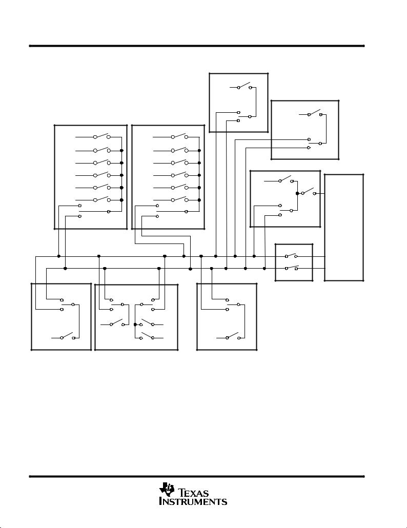
TMS370Cx5x
8-BIT MICROCONTROLLER
SPNS010F ± DECEMBER 1986 ± REVISED FEBRUARY 1997
interrupts (continued)
|
|
|
EXT INT 3 |
|
|
|
|
|
INT 3 |
|
|
|
|
|
|
EXT INT 2 |
|
TIMER 2A |
|
TIMER 1 |
|
INT 2 |
|
|
|
|
|
||
Overflow |
|
Overflow |
INT3 PRI |
|
|
|
|
|
|
||
Compare1 |
|
Compare1 |
|
|
|
Ext Edge |
|
Ext Edge |
|
INT2 PRI |
|
|
|
|
|
||
|
|
|
|
EXT INT1 |
CPU |
Compare2 |
|
Compare2 |
INT1 |
|
|
|
|
|
|
|
|
Input Capture 1 |
|
Input Capture 1 |
|
|
|
Input Capture 2 |
|
Watchdog |
|
|
NMI |
|
|
|
|
||
T2A PRI |
|
T1 PRI |
|
INT1 PRI |
Priority |
|
|
|
|
|
|
|
|
|
|
|
Logic |
|
|
|
|
STATUS REG |
|
|
|
|
|
IE1 |
|
|
|
|
|
IE2 |
Level 1 INT |
|
|
|
|
|
|
|
|
|
|
Enable |
Level 2 INT |
AD INT |
|
SCI INT |
SPI INT |
|
|
|
|
|
|||
AD PRI |
TX |
RX |
SPI PRI |
|
|
TXPRI |
RXPRI |
|
|
|
BRKDT |
|
|
TXRDY |
RXRDY |
|
|
A / D |
SPI |
||
|
Figure 4. Interrupt Control
On-chip peripheral functions generate six of the system interrupts. Three external interrupts also are supported. Software configuration of the external interrupts is performed through the INT1, INT2, and INT3 control registers in PF frame 1. Each external interrupt is individually software configurable for input polarity (rising or falling edge) for ease of system interface. External interrupt INT1 is software configurable as either a maskable or non-maskable interrupt. When INT1 is configured as nonmaskable, it cannot be masked by the individualor global-enable mask bits. The INT1 NMI bit is protected during non-privileged operation and, therefore, should be configured during the initialization sequence following reset. To maximize pin flexibility, external interrupts INT2 and INT3 can be software configured as general purpose input/output pins if the interrupt function is not required (INT1 can be similarly configured as an input pin). Table 12 shows the interrupt vector sources, corresponding addresses, and hardware priorities.
18 |
POST OFFICE BOX 1443 •HOUSTON, TEXAS 77251±1443 |

|
|
|
|
|
|
|
|
TMS370Cx5x |
|
|
|
|
|
|
|
|
8-BIT MICROCONTROLLER |
||
|
|
|
|
|
SPNS010F ± DECEMBER 1986 ± REVISED FEBRUARY 1997 |
||||
|
|
|
|
|
|
|
|
|
|
interrupts (continued) |
|
|
|
|
|
|
|
||
|
|
|
Table 12. Hardware System Interrupts |
|
|
|
|||
|
|
|
|
|
|
|
|
|
|
INTERRUPT SOURCE |
INTERRUPT FLAG |
SYSTEM |
VECTOR |
PRIORITY² |
|
||||
INTERRUPT |
ADDRESS |
|
|||||||
|
|
|
|
|
|
||||
|
|
|
|
|
|
|
|
|
|
External |
|
|
COLD START |
|
|
|
|
|
|
RESET |
|
|
|
³ |
|
|
|
||
Watchdog overflow |
WD OVRFL INT FLAG |
|
RESET |
7FFEh, 7FFFh |
1 |
|
|||
Oscillator fault detect |
OSC FLT FLAG |
|
|
|
|
|
|
||
|
|
|
|
|
|
|
|
|
|
External INT1 |
INT1 FLAG |
|
INT1³ |
7FFCh, 7FFDh |
2 |
|
|||
External INT2 |
INT2 FLAG |
|
INT2³ |
7FFAh, 7FFBh |
3 |
|
|||
External INT3 |
INT3 FLAG |
|
INT3³ |
7FF8h, 7FF9h |
4 |
|
|||
SPI RX/TX complete |
SPI INT FLAG |
|
SPIINT |
7FF6h, 7FF7h |
5 |
|
|||
|
|
|
|
|
|
|
|
||
Timer 1 overflow |
T1 OVRFL INT FLAG |
|
|
|
|
|
|
||
Timer 1 compare 1 |
T1C1 INT FLAG |
|
|
|
|
|
|
||
Timer 1 compare 2 |
T1C2 INT FLAG |
|
T1INT§ |
7FF4h, 7FF5h |
6 |
|
|||
Timer 1 external edge |
T1EDGE INT FLAG |
|
|
||||||
|
|
|
|
|
|
||||
Timer 1 input capture 1 |
T1IC1 INT FLAG |
|
|
|
|
|
|
||
Watchdog overflow |
WD OVRFL INT FLAG |
|
|
|
|
|
|
||
|
|
|
|
|
|
|
|
||
SCI RX data register full |
RXRDY FLAG |
|
RXINT³ |
7FF2h,7FF3h |
7 |
|
|||
SCI RX break detect |
BRKDT FLAG |
|
|
||||||
|
|
|
|
|
|
||||
|
|
|
|
|
|
|
|||
SCI TX data register empty |
TXRDY FLAG |
|
TXINT |
7FF0h, 7FF1h |
8 |
|
|||
|
|
|
|
|
|
|
|
||
Timer 2A overflow |
T2A OVRFL INT FLAG |
|
|
|
|
|
|
||
Timer 2A compare 1 |
T2AC1 INT FLAG |
|
|
|
|
|
|
||
Timer 2A compare 2 |
T2AC2 INT FLAG |
|
T2AINT |
7FEEh, 7FEFh |
9 |
|
|||
Timer 2A external edge |
T2AEDGE INT FLAG |
|
|
||||||
|
|
|
|
|
|
||||
Timer 2A input capture 1 |
T2AIC1 INT FLAG |
|
|
|
|
|
|
||
Timer 2A input capture 2 |
T2AIC2 INT FLAG |
|
|
|
|
|
|
||
|
|
|
|
|
|
|
|||
A/D conversion complete |
AD INT FLAG |
|
ADINT |
7FECh, 7FEDh |
10 |
|
|||
² Relative priority within an interrupt level |
|
|
|
|
|
|
|
||
³ Releases microcontroller from STANDBY and HALT low-power modes. § Releases microcontroller from STANDBY low-power mode.
privileged operation and EEPROM write-protection override
The TMS370Cx5x family has significant flexibility to enable the designer to software-configure the system and peripherals to meet the requirements of a broad variety of applications. The nonprivileged mode of operation ensures the integrity of the system configuration, once it is defined for an application. Following a hardware reset, the TMS370Cx5x operates in the privileged mode, where all peripheral file registers have unrestricted read/write access, and the application program configures the system during the initialization sequence following reset. As the last step of system initialization, the PRIVILEGE DISABLE bit (SCCR2.0) should be set to 1 to enter the nonprivileged mode; disabling write operations to specific configuration control bits within the peripheral file. Table 13 displays the system configuration bits that are write-protected during the nonprivileged mode and must be configured by software prior to exiting the privileged mode.
POST OFFICE BOX 1443 •HOUSTON, TEXAS 77251±1443 |
19 |

TMS370Cx5x
8-BIT MICROCONTROLLER
SPNS010F ± DECEMBER 1986 ± REVISED FEBRUARY 1997
privileged operation and EEPROM write-protection override (continued)
Table 13. Privileged Bits
REGISTER² |
CONTROL BIT |
||
NAME |
LOCATION |
||
|
|||
|
|
|
|
SCCRO |
P010.5 |
PF AUTOWAIT |
|
P010.6 |
OSC POWER |
||
|
|||
|
|
|
|
SCCR1 |
P011.2 |
MEMORY DISABLE |
|
P011.4 |
AUTOWAIT DISABLE |
||
|
|||
|
|
|
|
|
P012.0 |
PRIVILEGE DISABLE |
|
|
P012.1 |
INT1 NMI |
|
SCCR2 |
P012.3 |
CPU STEST |
|
P012.4 |
BUS STEST |
||
|
|||
|
P012.6 |
PWRDWN/IDLE |
|
|
P012.7 |
HALT/STANDBY |
|
|
|
|
|
|
P03F.5 |
SPI ESPEN |
|
SPIPRI |
P03F.6 |
SPI PRIORITY |
|
|
P03F.7 |
SPI STEST |
|
|
|
|
|
|
P05F.4 |
SCI ESPEN |
|
SCIPRI |
P05F.5 |
SCIRX PRIORITY |
|
P05F.6 |
SCITX PRIORITY |
||
|
|||
|
P05F.7 |
SCI STEST |
|
|
|
|
|
T1PRI |
P04F.6 |
T1 PRIORITY |
|
P04F.7 |
T1 STEST |
||
|
|||
|
|
|
|
T2APRI |
P06F.6 |
T2A PRIORITY |
|
P06F.7 |
T2A STEST |
||
|
|||
|
|
|
|
|
P07F.5 |
AD ESPEN |
|
ADPRI |
P07F.6 |
AD PRIORITY |
|
|
P07F.7 |
AD STEST |
|
|
|
|
|
² The privileged bits are shown in a bold typeface in Table 15.
The write-protect override (WPO) mode provides an external hardware method for overriding the write-protection registers of data EEPROM on the TMS370Cx5x. The WPO mode is entered by applying a 12-V input to MC after RESET input goes high (logic 1). The high voltage on MC during the WPO mode is not the programming voltage for the data EEPROM or Program EPROM. All EEPROM programming voltages are generated on-chip. The WPO mode provides hardware system-level capability to modify the content of the data EEPROM while the device remains in the application, but only while requiring a 12-V external input on the MC pin (normally not available in the end application except in a service or diagnostic environment).
low-power and IDLE modes
The TMS370Cx5x devices have two low-power modes (STANDBY and HALT) and an IDLE mode. For mask-ROM devices, low-power modes can be disabled permanently through a programmable contact at the time when the mask is manufactured.
The STANDBY and HALT low power modes significantly reduce power consumption by reducing or stopping the activity of the various on-chip peripherals when processing is not required. Each of the low-power modes is entered by executing the IDLE instruction when the PWRDWN/IDLE bit in SCCR2 has been set to 1. The HALT/STANDBY bit in SCCR2 controls which low-power mode is entered.
In the STANDBY mode (HALT/STANDBY = 0), all CPU activity and most peripheral module activity is stopped; however, the oscillator, internal clocks, timer 1, and the receive start-bit detection circuit of the serial communications interface remain active. System processing is suspended until a qualified interrupt (hardware RESET, external interrupt on INT1, INT2, INT3, timer 1 interrupt, or low level on the receive pin of the serial communications interface 1) is detected.
20 |
POST OFFICE BOX 1443 •HOUSTON, TEXAS 77251±1443 |
TMS370Cx5x
8-BIT MICROCONTROLLER
SPNS010F ± DECEMBER 1986 ± REVISED FEBRUARY 1997
low-power and IDLE modes (continued)
In the HALT mode (HALT/STANDBY = 1), the TMS370Cx5x is placed in its lowest power consumption mode. The oscillator and internal clocks are stopped, causing all internal activity to be halted. System activity is suspended until a qualified interrupt (hardware RESET, external interrupt on the INT1, INT2, INT3, or low level on the receive pin of the serial communications interface 1) is detected. The low-power mode selection bits are summarized in Table 14.
Table 14. Low-Power/Idle Control Bits
POWER-DOWN CONTROL BITS |
|
|
|
|
MODE SELECTED |
PWRDWN/IDLE |
HALT/STANDBY |
|
(SCCR2.6) |
(SCCR2.7) |
|
|
|
|
1 |
0 |
STANDBY |
|
|
|
1 |
1 |
HALT |
|
|
|
0 |
X |
IDLE |
X = don't care
When low-power modes are disabled through a programmable contact in the mask-ROM devices, writing to the SCCR2.6±7 bits is ignored. In addition, if an idle instruction is executed when low-power modes are disabled through a programmable contact, the device always enters the IDLE mode.
To provide a method of always exiting low-power modes for mask-ROM devices, INT1 is enabled automatically as a nonmaskable interrupt (NMI) during low-power modes when the hard watchdog mode is selected. This means that the NMI is generated always, regardless of the interrupt enable flags.
The following information is preserved throughout both the STANDBY and HALT modes: RAM (register file), CPU registers (stack pointer, program counter, and status register), I/O pin direction and output data, and status registers of all on-chip peripheral functions. Since all CPU instruction processing is stopped during the STANDBY and HALT modes, the clocking of the watchdog timer is inhibited.
clock modules
The `x5x family provides two clock options which are referred to as divide-by-1 (PLL) and divide-by-4 (standard oscillator). Both the divide-by-1 and divide-by-4 options are configurable during the manufacturing process of a TMS370 microcontroller. The `x5x ROM-masked devices offer both options to meet system engineering requirements. Only one of the two clock options is allowed on each ROM device. The `75xA EPROM has only the standard divide-by-4, while the `75xB EPROM has the divide-by-1.
The divide-by-1 clock module option provides the capability for reduced electromagnetic interference (EMI) with no added cost.
The divide-by-1 provides a 1-to-1 match of the external resonator frequency to the internal system clock (SYSCLK) frequency. The divide-by-4 produces a SYSCLK which is one-fourth the frequency of the external resonator. Inside the divide-by-1 module, the frequency of the external resonator is multiplied by four. The clock module then divides the resulting signal by four to provide the four-phased internal system clock signals. The resulting SYSCLK is equal to the resonator frequency. The frequencies are formulated as follows
Divide-by-4 |
option : SYSCLK + |
external resonator frequency |
|
+ CLKIN |
|
|
|||||
|
4 |
|
4 |
||
Divide-by-1 |
option : SYSCLK + |
external resonator frequency |
4 |
+ CLKIN |
|
|
|
||||
|
4 |
|
|
|
|
The main advantage of choosing a divide-by-1 oscillator is the improved EMI performance. The harmonics of low-speed resonators extend through less of the emissions spectrum than the harmonics of faster resonators. The divide-by-1 provides the capability of reducing the resonator speed by four times, and this results in a steeper decay of emissions produced by the oscillator.
POST OFFICE BOX 1443 •HOUSTON, TEXAS 77251±1443 |
21 |

TMS370Cx5x
8-BIT MICROCONTROLLER
SPNS010F ± DECEMBER 1986 ± REVISED FEBRUARY 1997
system configuration registers
Table 15 contains system configuration and control functions and registers for controlling EEPROM programming. The privileged bits are shown in a bold typeface and shaded.
Table 15. Peripheral File Frame 1: System Configuration Registers
PF |
BIT 7 |
BIT 6 |
BIT 5 |
BIT 4 |
BIT 3 |
BIT 2 |
BIT 1 |
BIT 0 |
REG |
|
|
|
|
|
|
|
|
|
|
|
|
P010 |
COLD |
OSC |
PF AUTO |
OSC FLT |
MC PIN |
MC PIN |
Ð |
P/C |
SCCR0 |
|
START |
POWER |
WAIT |
FLAG |
WPO |
DATA |
MODE |
||||
|
|
|
||||||||
P011 |
Ð |
Ð |
Ð |
AUTOWAIT |
Ð |
MEMORY |
Ð |
Ð |
SCCR1 |
|
DISABLE |
DISABLE |
|||||||||
|
|
|
|
|
|
|
|
|||
P012 |
HALT/ |
PWRDWN/ |
Ð |
BUS |
CPU |
Ð |
INT1 |
PRIVILEGE |
SCCR2 |
|
STANDBY |
IDLE |
STEST |
STEST |
NMI |
DISABLE |
|||||
|
|
|
|
|||||||
P013 |
|
|
|
Reserved |
|
|
|
|
||
|
|
|
|
|
|
|
|
|
|
|
P014 |
BUSY |
VPPS |
Ð |
Ð |
Ð |
Ð |
W0 |
EXE |
EPCTLH |
|
P015 |
|
|
|
|
|
|
|
|
|
|
|
|
|
|
|
|
|
|
|
||
to |
|
|
|
Reserved |
|
|
|
|
||
P016 |
|
|
|
|
|
|
|
|
|
|
|
|
|
|
|
|
|
|
|
|
|
P017 |
INT1 |
INT1 |
Ð |
Ð |
Ð |
INT1 |
INT1 |
INT1 |
INT1 |
|
FLAG |
PIN DATA |
POLARITY |
PRIORITY |
ENABLE |
||||||
|
|
|
|
|
||||||
|
|
|
|
|
|
|
|
|
|
|
P018 |
INT2 |
INT2 |
Ð |
INT2 |
INT2 |
INT2 |
INT2 |
INT2 |
INT2 |
|
FLAG |
PIN DATA |
DATA DIR |
DATA OUT |
POLARITY |
PRIORITY |
ENABLE |
||||
|
|
|
||||||||
|
|
|
|
|
|
|
|
|
|
|
P019 |
INT3 |
INT3 |
Ð |
INT3 |
INT3 |
INT3 |
INT3 |
INT3 |
INT3 |
|
FLAG |
PIN DATA |
DATA DIR |
DATA OUT |
POLARITY |
PRIORITY |
ENABLE |
||||
|
|
|
||||||||
|
|
|
|
|
|
|
|
|
|
|
P01A |
BUSY |
Ð |
Ð |
Ð |
Ð |
AP |
W1W0 |
EXE |
DEECTL |
|
|
|
|
|
|
|
|
|
|
|
|
P01B |
|
|
|
Reserved |
|
|
|
|
||
|
|
|
|
|
|
|
|
|
|
|
P01C |
BUSY |
VPPS |
Ð |
Ð |
Ð |
Ð |
W0 |
EXE |
EPCTLM |
|
|
|
|
|
|
|
|
|
|
|
|
P01D |
|
|
|
Reserved |
|
|
|
|
||
|
|
|
|
|
|
|
|
|
|
|
P01E |
BUSY |
VPPS |
Ð |
Ð |
Ð |
Ð |
W0 |
EXE |
EPCTLL |
|
|
|
|
|
|
|
|
|
|
|
|
P01F |
|
|
|
Reserved |
|
|
|
|
||
|
|
|
|
|
|
|
|
|
|
|
|
|
|
|
|
|
|
|
|
|
|
22 |
POST OFFICE BOX 1443 •HOUSTON, TEXAS 77251±1443 |

TMS370Cx5x
8-BIT MICROCONTROLLER
SPNS010F ± DECEMBER 1986 ± REVISED FEBRUARY 1997
digital port control registers
Peripheral file frame 2 contains the digital I/O pin configuration and control registers. Table 16 lists the specific addresses, registers, and control bits within this peripheral file frame.
Table 16. Peripheral File Frame 2: Digital Port Control Registers
PF |
BIT 7 |
BIT 6 |
BIT 5 |
BIT 4 |
BIT 3 |
BIT 2 |
BIT 1 |
BIT 0 |
REG |
|
|
|
|
|
|
|
|
|
|
P020 |
|
|
|
Reserved |
|
|
|
APORT1 |
|
|
|
|
|
|
|
|
|
|
|
P021 |
|
|
|
Port A Control Register 2 |
|
|
|
APORT2 |
|
|
|
|
|
|
|
|
|
|
|
P022 |
|
|
|
Port A Data |
|
|
|
ADATA |
|
|
|
|
|
|
|
|
|
|
|
P023 |
|
|
|
Port A Direction |
|
|
|
ADIR |
|
|
|
|
|
|
|
|
|
|
|
P024 |
|
|
|
Reserved |
|
|
|
BPORT1 |
|
|
|
|
|
|
|
|
|
|
|
P025 |
|
|
|
Port B Control Register 2 |
|
|
|
BPORT2 |
|
|
|
|
|
|
|
|
|
|
|
P026 |
|
|
|
Port B Data |
|
|
|
BDATA |
|
|
|
|
|
|
|
|
|
|
|
P027 |
|
|
|
Port B Direction |
|
|
|
BDIR |
|
|
|
|
|
|
|
|
|
|
|
P028 |
|
|
|
Reserved |
|
|
|
CPORT1 |
|
|
|
|
|
|
|
|
|
|
|
P029 |
|
|
|
Port C Control Register 2 |
|
|
|
CPORT2 |
|
|
|
|
|
|
|
|
|
|
|
P02A |
|
|
|
Port C Data |
|
|
|
CDATA |
|
|
|
|
|
|
|
|
|
|
|
P02B |
|
|
|
Port C Direction |
|
|
|
CDIR |
|
|
|
|
|
|
|
|
|
|
|
P02C |
|
|
|
Port D Control Register 1 |
|
|
|
DPORT1 |
|
|
|
|
|
|
|
|
|
|
|
P02D |
|
|
|
Port D Control Register 2² |
|
|
|
DPORT2 |
|
P02E |
|
|
|
Port D Data |
|
|
|
DDATA |
|
|
|
|
|
|
|
|
|
|
|
P02F |
|
|
|
Port D Direction |
|
|
|
DDIR |
|
|
|
|
|
|
|
|
|
|
|
² To configure pin D3 as SYSCLK, set port D control register 2 = 08h.
POST OFFICE BOX 1443 •HOUSTON, TEXAS 77251±1443 |
23 |
TMS370Cx5x
8-BIT MICROCONTROLLER
SPNS010F ± DECEMBER 1986 ± REVISED FEBRUARY 1997
digital port control registers (continued)
Table 17. Port Configuration Register Setup
|
|
INPUT |
OUTPUT |
FUNCTION A |
FUNCTION B |
|||||||
|
|
( P MODE) |
||||||||||
|
|
|
|
|
|
|
|
|||||
|
|
|
|
|
|
|
|
|
|
|
|
|
PORT |
PIN |
XPORT1 = 0² |
XPORT1 = 0² |
XPORT1 = 0² |
XPORT1 = 1² |
|||||||
XPORT2 = 0 |
XPORT2 = 0 |
XPORT2 = 1 |
XPORT2 = 1 |
|||||||||
|
|
|||||||||||
|
|
XDATA = y |
XDATA = q |
XDATA = x |
XDATA = x |
|||||||
|
|
XDIR = 0 |
XDIR = 1 |
XDIR = x |
XDIR = x |
|||||||
|
|
|
|
|
|
|
|
|
|
|
|
|
A |
0 ± 7 |
Data In y |
Data Out q |
Data Bus |
Reserved |
|||||||
|
|
|
|
|
|
|
|
|
|
|
|
|
B |
0 ± 7 |
Data In y |
Data Out q |
Low ADDR |
Reserved |
|||||||
|
|
|
|
|
|
|
|
|
|
|
|
|
C |
0 ± 7 |
Data In y |
Data Out q |
Hi ADDR |
Reserved |
|||||||
|
|
|
|
|
|
|
|
|
|
|
||
|
0 |
|
|
|
|
|
|
|
|
|
|
|
|
|
|
|
CSE2 |
|
|
|
OCF |
|
|||
|
1 |
|
|
CSH3 |
Ð |
|
|
|||||
|
2 |
|
|
CSH2 |
Ð |
|
|
|||||
D |
3 |
Data In y |
Data Out q |
SYSCLK |
SYSCLK |
|||||||
4 |
|
R / W |
|
R/W |
||||||||
|
|
|
|
|
||||||||
|
5 |
|
|
|
CSPF |
|
Ð |
|
|
|||
|
6 |
|
|
CSH1 |
|
EDS |
|
|||||
|
7 |
|
|
|
CSE1 |
WAIT |
||||||
|
|
|
|
|
|
|
|
|
|
|
|
|
XPORT1 = 1
XPORT2 =0
Not defined
XDATA = x
XDIR = x
² DPORT only
timer 1 module
The programmable timer 1 (T1) module of the TMS370Cx5x provides the designer with the enhanced timer resources required to perform realtime system control. The T1 module contains the general-purpose timer and the watchdog (WD) timer. The two independent 16-bit timers (T1 and WD) allow program selection of input clock sources (real-time, external event, or pulse-accumulate) with multiple 16-bit registers (input capture and compare) for special timer function control. The T1 module includes three external device pins that can be used for multiple counter functions (operation mode dependent) or used as general-purpose I/O pins. T1 module is shown in Figure 5.
24 |
POST OFFICE BOX 1443 •HOUSTON, TEXAS 77251±1443 |
 Loading...