


TMS320LC2406

现货库存、技术资料、百科信息、热点资讯,精彩尽在鼎好!
TMS320LF2407, TMS320LF2406, TMS320LF2402
TMS320LC2406, TMS320LC2404, TMS320LC2402
DSP CONTROLLERS
SPRS094C – APRIL 1999 – REVISED OCTOBER 1999
1
POST OFFICE BOX 1443 • HOUSTON, TEXAS 77251–1443
D High-Performance Static CMOS Technology
– 33-ns Instruction Cycle Time (30 MHz)
– 30 MIPS Performance
– Low-Power 3.3-V Design
D Based on T320C2xx DSP CPU Core
– Code-Compatible With ’F243/’F241/’C242
– Instruction Set and Module Compatible
With ’F240/’C240
– Source-Code-Compatible With
TMS320C1x/2x
D Flash (LF) and ROM (LC) Device Options
– ’LF240x
†
: ’LF2407, ’LF2406, ’LF2402
– ’LC240x
†
: ’LC2406, ’LC2404, ’LC2402
D On-Chip Memory
– Up to 32K Words x 16 Bits of Flash
EEPROM (4 Sectors) or ROM
– Up to 2.5K Words x 16 Bits of
Data/Program RAM
– 544 Words of Dual-Access (DARAM)
– 2K Words of Single-Access (SARAM)
D Boot ROM (’LF240x Devices)
– SCI/SPI Flash Bootloader
D Two Event-Manager (EV) Modules (A and B)
EVA and EVB Each Include:
– Two 16-Bit General-Purpose Timers
– Eight 16-Bit Pulse-Width Modulation
(PWM) Channels Which Enable:
– Three-Phase Inverter Control
– Centered or Edge Alignment of PWM
Channels
– Emergency PWM Channel Shutdown
With External PDPINT
Pin
– Programmable Deadband Prevents
Shoot-Through Faults
– Three Capture Units For Time-Stamping
of External Events
– On-Chip Position Encoder Interface
Circuitry
– Synchronized Analog-to-Digital
Conversion
– Suitable for AC Induction, BLDC,
Switched Reluctance, and Stepper Motor
Control
– Applicable for Multiple Motor and/or
Converter Control
D External Memory Interface (’LF2407)
– 192K Words x 16 Bits of Total Memory,
64K Program, 64K Data, 64K I/O
D Watchdog (WD) Timer Module
D 10-Bit Analog-to-Digital Converter (ADC)
– 8 or 16 Multiplexed Input Channels
– 500 ns Minimum Conversion Time
– Selectable Twin 8-Input Sequencers
Triggered by Two Event Managers
D Controller Area Network (CAN) 2.0B Module
D Serial Communications Interface (SCI)
D 16-Bit Serial Peripheral Interface (SPI)
Module (Except ’x2402)
D Phase-Locked-Loop (PLL)-Based Clock
Generation
D Up to 40 Individually Programmable,
Multiplexed General-Purpose Input/Output
(GPIO) Pins
D Five External Interrupts (Power Drive
Protection, Reset, and Two Maskable
Interrupts)
D Power Management:
– Three Power-Down Modes
– Ability to Power-Down Each Peripheral
Independently
D Real-Time JTAG-Compliant Scan-Based
Emulation, IEEE Standard 1149.1
‡
(JTAG)
D Development Tools Include:
– Texas Instruments (TI) ANSI
C Compiler, Assembler/Linker, and
Code Composer Debugger
– Evaluation Modules
– Scan-Based Self-Emulation (XDS510)
– Numerous Third-Party Digital Motor
Control Support
D Package Options
– 144-Pin Thin Quad Flatpack (TQFP) PGE
(’LF2407)
– 100-Pin TQFP PZ (’LC2404, ’LC2406,
’LF2406)
– 64-Pin PQFP PG (’LC2402 and ’LF2402)
D Extended Temperature Options (A and S)
– A: – 40°C to 85°C
– S: – 40°C to 125°C
ADVANCE
INFORMATION
Copyright 1999, Texas Instruments Incorporated
Please be aware that an important notice concerning availability, standard warranty, and use in critical applications of
Texas Instruments semiconductor products and disclaimers thereto appears at the end of this data sheet.
TI, Code Composer, and XDS510 are trademarks of Texas Instruments Incorporated.
†
Throughout this data sheet, ’240x is used as a generic name for the ’LF240x/’LC240x family of devices.
‡
IEEE Standard 1149.1–1990, IEEE Standard Test-Access Port
ADVANCE INFORMATION concerns new products in the sampling or
preproduction phase of development. Characteristic data and other
specifications are subject to change without notice.

TMS320LF2407, TMS320LF2406, TMS320LF2402
TMS320LC2406, TMS320LC2404, TMS320LC2402
DSP CONTROLLERS
SPRS094C – APRIL 1999 – REVISED OCTOBER 1999
2
POST OFFICE BOX 1443 • HOUSTON, TEXAS 77251–1443
Description 2. . . . . . . . . . . . . . . . . . . . . . . . . . . . . . . . . . . . .
TMS320x240x Device Summary 3. . . . . . . . . . . . . . . . . . .
Functional Block Diagram of the ’2407 DSP Controller 4
Pin Functions 8. . . . . . . . . . . . . . . . . . . . . . . . . . . . . . . . . . .
Memory Maps 15. . . . . . . . . . . . . . . . . . . . . . . . . . . . . . . . .
Peripheral Memory Map of the ’LF240x/’LC240x 21. . . .
Device Reset and Interrupts 22. . . . . . . . . . . . . . . . . . . . .
TMS320x240x Instruction Set 26. . . . . . . . . . . . . . . . . . . .
Functional Block Diagram
of the ’240x DSP CPU 27. . .
Peripherals 36. . . . . . . . . . . . . . . . . . . . . . . . . . . . . . . . . . . .
Event Manager Modules (EV A, EVB) 36. . . . . . . . . . . .
Enhanced Analog-to-Digital Converter
(ADC) Module 40. . . . . . . . . . . . . . . . . . . . . . . . . . . .
Controller Area Network (CAN) Module 41. . . . . . . . . .
Serial Communications Interface (SCI) Module 44. . . .
Serial Peripheral Interface (SPI) Module 46. . . . . . . . . .
PLL-Based Clock Module 48. . . . . . . . . . . . . . . . . . . . . .
Digital I/O and Shared Pin Functions 51. . . . . . . . . . . . .
External Memory Interface (’LF2407) 54. . . . . . . . . . . .
Watchdog (WD) Timer Module 55. . . . . . . . . . . . . . . . . .
Development Support 58. . . . . . . . . . . . . . . . . . . . . . . . . . .
Documentation Support 61. . . . . . . . . . . . . . . . . . . . . . . . .
Absolute Maximum Ratings 62. . . . . . . . . . . . . . . . . . . . . .
Recommended Operating Conditions 62. . . . . . . . . . . . .
Peripheral Register Description 90. . . . . . . . . . . . . . . . . . .
Mechanical Data 103. . . . . . . . . . . . . . . . . . . . . . . . . . . . . .
Table of Contents
description
The TMS320LF240x and TMS320LC240x devices, new members of the ’24x family of digital signal processor
(DSP) controllers, are part of the C2000 platform of fixed-point DSPs. The ’240x devices offer the enhanced
TMS320 architectural design of the ’C2xx core CPU for low-cost, low-power, high-performance processing
capabilities. Several advanced peripherals, optimized for digital motor and motion control applications, have
been integrated to provide a true single chip DSP controller. While code-compatible with the existing ’24x DSP
controller devices, the ’240x offers increased processing performance (30 MIPS) and a higher level of peripheral
integration. See the TMS320x240x device summary section for device-specific features.
The ’240x family offers an array of memory sizes and different peripherals tailored to meet the specific
price/performance points required by various applications. Flash-based devices of up to 32K words offer a
reprogrammable solution useful for:
– Applications requiring field programmability upgrades
– Development and initial prototyping of applications that migrate to ROM-based devices
Flash devices and corresponding ROM devices are fully pin-to-pin compatible. Note that flash-based devices
contain a 256-word boot ROM to facilitate in-circuit programming.
All ’240x devices offer at least one event manager module which has been optimized for digital motor control
and power conversion applications. Capabilities of this module include centered- and/or edge-aligned PWM
generation, programmable deadband to prevent shoot-through faults, and synchronized analog-to-digital
conversion. Devices with dual event managers enable multiple motor and/or converter control with a single
’240x DSP controller.
The high performance, 10-bit analog-to-digital converter (ADC) has a minimum conversion time of 500 ns and
offers up to 16 channels of analog input. The auto sequencing capability of the ADC allows a maximum of
16 conversions to take place in a single conversion session without any CPU overhead.
A serial communications interface (SCI) is integrated on all devices to provide asynchronous communication
to other devices in the system. For systems requiring additional communication interfaces; the ’2407, ’2406,
and ’2404 offer a 16-bit synchronous serial peripheral interface (SPI). The ’2407 and ’2406 offer a controller area
network (CAN) communications module that meets 2.0B specifications. To maximize device flexibility,
functional pins are also configurable as general purpose inputs/outputs (GPIO).
To streamline development time, JTAG-compliant scan-based emulation has been integrated into all devices.
This provides non-intrusive real-time capabilities required to debug digital control systems. A complete suite
of code generation tools from C compilers to the industry-standard Code Composer debugger supports this
family. Numerous third party developers not only offer device-level development tools, but also system-level
design and development support.
ADVANCE
INFORMATION
TMS320LF2407, TMS320LF2406, TMS320LF2402
TMS320LC2406, TMS320LC2404, TMS320LC2402
DSP CONTROLLERS
SPRS094C – APRIL 1999 – REVISED OCTOBER 1999
3
POST OFFICE BOX 1443 • HOUSTON, TEXAS 77251–1443
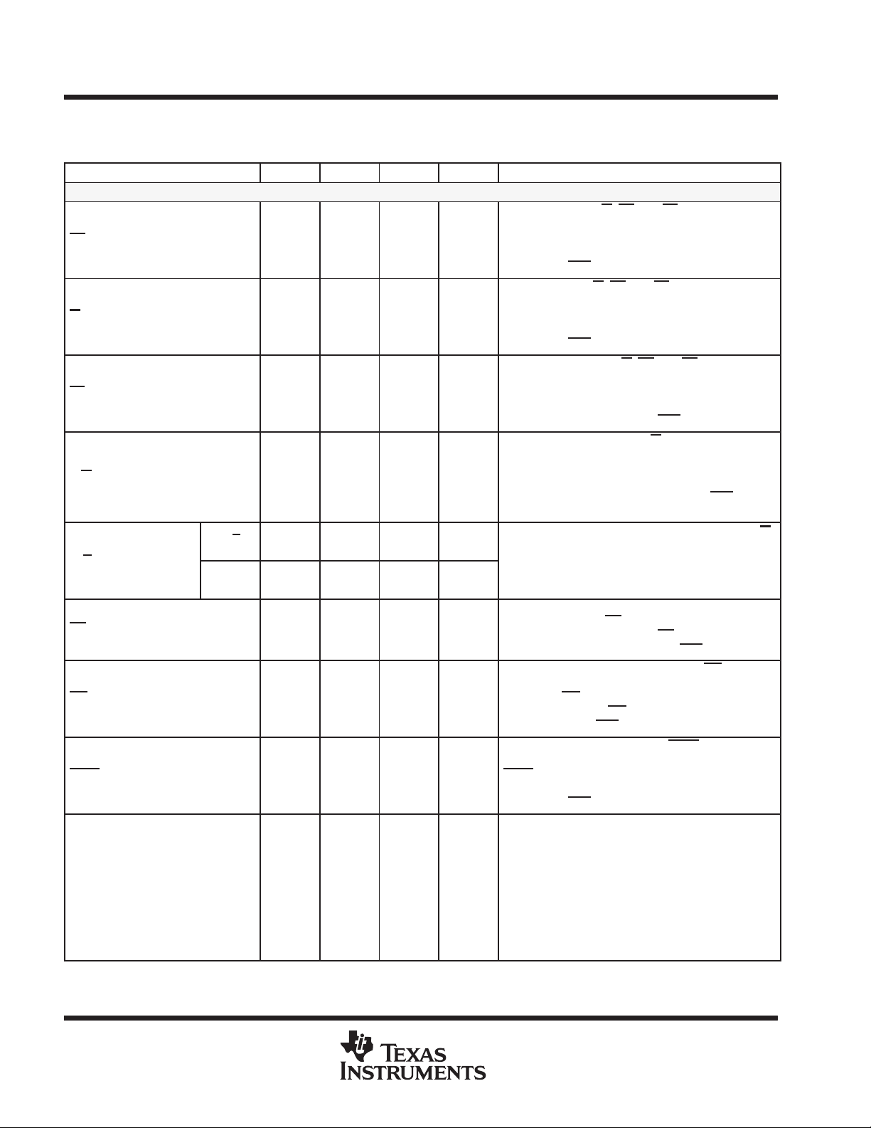
TMS320x240x device summary
Note that throughout this data sheet, ’240x is used as a generic name for the ’LF240x/’LC240x family of devices.
Table 1. Hardware Features of ’240x Devices
FEATURE ’LF2407
†
’LF2406 ’LF2402 ’LC2406 ’LC2404 ’LC2402
’C2xx DSP Core Yes Yes Yes Yes Yes Yes
Instruction Cycle 33 ns 33 ns 33 ns 33 ns 33 ns 33 ns
MIPS (30 MHz) 30 MIPS 30 MIPS 30 MIPS 30 MIPS 30 MIPS 30 MIPS
DARAM 544 544 544 544 544 544
RAM (16-bit word)
SARAM 2K 2K — 2K 1K —
On-chip Flash (16-bit word)
(4 sectors: 4K, 12K, 12K, 4K)
32K 32K 8K — — —
On-chip ROM (16-bit word) — — — 32K 16K 4K
Boot ROM (16-bit word) 256 256 256 — — —
External Memory Interface Yes — — — — —
Event Managers A and B
(EVA and EVB)
EVA, EVB EVA, EVB EVA EVA, EVB EVA, EVB EVA
S General-Purpose (GP) Timers 4 4 2 4 4 2
S Compare (CMP)/PWM 10/16 10/16 5/8 10/16 10/16 5/8
S Capture (CAP)/QEP 6/4 6/4 3/2 6/4 6/4 3/2
Watchdog Timer Yes Yes Yes Yes Yes Yes
10-Bit ADC Yes Yes Yes Yes Yes Yes
S Channels 16 16 8 16 16 8
S Conversion Time (minimum) 500 ns 500 ns 500 ns 500 ns 500 ns 500 ns
SPI Yes Yes — Yes Yes —
SCI Yes Yes Yes Yes Yes Yes
CAN Yes Yes — Yes — —
Digital I/O Pins (Shared) 41 41 21 41 41 21
External Interrupts 5 5 3 5 5 3
Supply Voltage 3.3 V 3.3 V 3.3 V 3.3 V 3.3 V 3.3 V
Packaging 144 TQFP 100 TQFP 64 PQFP 100 TQFP 100 TQFP 64 PQFP
†
’LF2407, the full-featured device of the ’LF240x family of DSP controllers, is useful for emulation and code development.
ADVANCE
INFORMATION
TMS320LF2407, TMS320LF2406, TMS320LF2402
TMS320LC2406, TMS320LC2404, TMS320LC2402
DSP CONTROLLERS
SPRS094C – APRIL 1999 – REVISED OCTOBER 1999
4
POST OFFICE BOX 1443 • HOUSTON, TEXAS 77251–1443
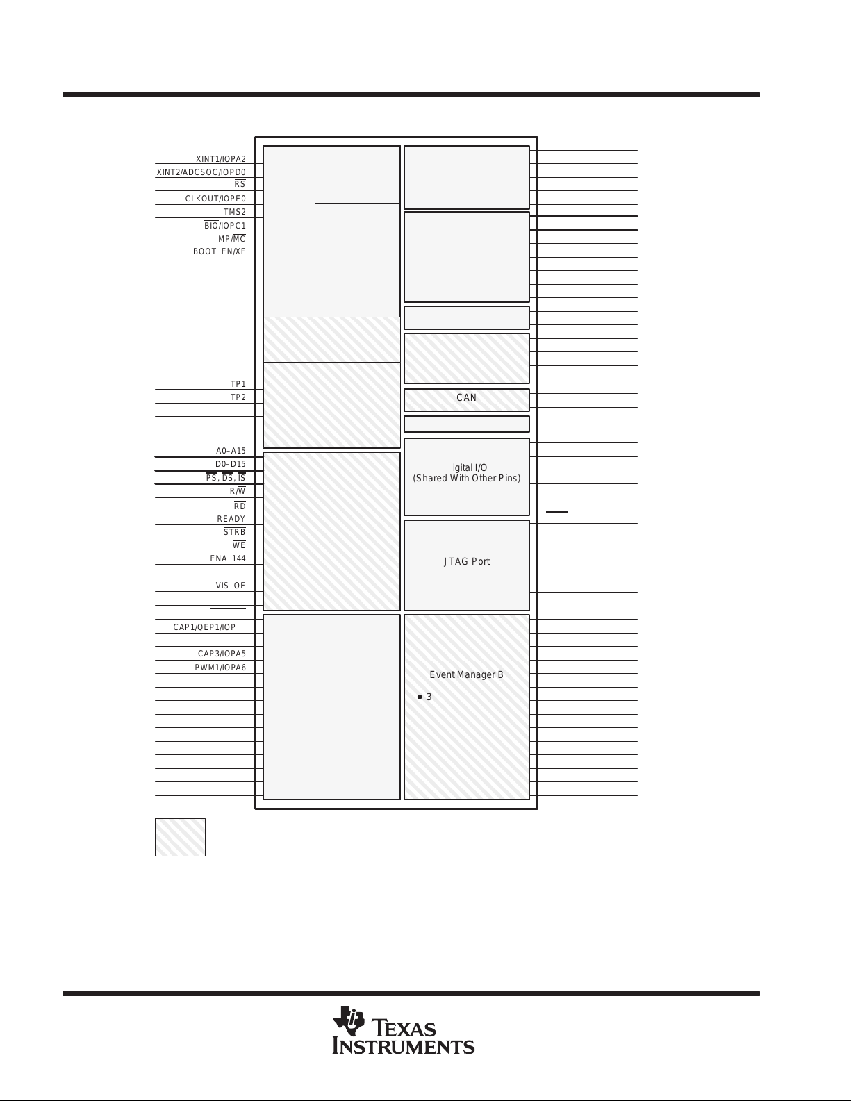
functional block diagram of the ’2407 DSP controller
XTAL1/CLKIN
XTAL2
PLLV
CCA
PLLF2
PLLF
V
SSA
V
REFHI
ADCIN08–ADCIN15
V
CCA
ADCIN00–ADCIN07
SCIRXD/IOPA1
SPISIMO/IOPC2
XINT2/ADCSOC/IOPD0
SCITXD/IOPA0
V
REFLO
V
CCP
(5V)
Port A(0–7) IOPA[0:7]
SPICLK/IOPC4
SPISTE/IOPC5
SPISOMI/IOPC3
Port E(0–7) IOPE[0:7]
Port F(0–6) IOPF[0:6]
Port C(0–7) IOPC[0:7]
Port D(0) IOPD[0]
Port B(0–7) IOPB[0:7]
TDO
TDI
CANRX/IOPC7
TRST
CANTX/IOPC6
EMU1
PDPINTB
TCK
EMU0
TMS
CAP5/QEP4/IOPF0
CAP4/QEP3/IOPE7
PWM7/IOPE1
PWM8/IOPE2
CAP6/IOPF1
PWM10/IOPE4
PWM9/IOPE3
PWM11/IOPE5
PWM12/IOPE6
T4PWM/T4CMP/IOPF3
T3PWM/T3CMP/IOPF2
TDIRB/IOPF4
TCLKINB/IOPF5
DARAM (B0)
256 Words
DARAM (B1)
256 Words
DARAM (B2)
32 Words
’C2xx
DSP
Core
PLL Clock
10-Bit ADC
(With Twin
Autosequencer)
RS
CLKOUT/IOPE0
XINT1/IOPA2
XINT2/ADCSOC/IOPD0
BIO/IOPC1
MP/MC
TMS2
A0–A15
D0–D15
TP1
TP2
BOOT_EN/XF
READY
STRB
R/W
RD
PS, DS, IS
VIS_OE
ENA_144
WE
CAP3/IOPA5
PWM1/IOPA6
CAP1/QEP1/IOPA3
CAP2/QEP2/IOPA4
PDPINTA
PWM5/IOPB2
PWM6/IOPB3
PWM3/IOPB0
PWM4/IOPB1
PWM2/IOPA7
T2PWM/T2CMP/IOPB5
T1PWM/T1CMP/IOPB4
TCLKINA/IOPB7
TDIRA/IOPB6
V
DD
(3.3 V)
V
SS
V
CCP
(5V)
SARAM (2K Words)
Flash/ROM
(32K Words:
4K/12K/12K/4K)
External Memory Interface
Event Manager A
D 3 × Capture Input
D 6 × Compare/PWM
Output
D 2 × GP Timers/PWM
SCI
SPI
WD
Digital I/O
(Shared With Other Pins)
CAN
JTAG Port
Event Manager B
D 3 × Capture Input
D 6 × Compare/PWM
Output
D 2 × GP Timers/PWM
Indicates optional modules
The memory size and peripheral selection of these modules change for different ’240x devices. See
Table 1 for device-specific details.
W/R / IOPC0
ADVANCE
INFORMATION
TMS320LF2407, TMS320LF2406, TMS320LF2402
TMS320LC2406, TMS320LC2404, TMS320LC2402
DSP CONTROLLERS
SPRS094C – APRIL 1999 – REVISED OCTOBER 1999
5
POST OFFICE BOX 1443 • HOUSTON, TEXAS 77251–1443
144
143
142
141
140
139
138
137
136
135
134
RS
133
132
131
130
129
128
127
126
125
124
123
122
121
120
119
118
117
116
115
114
113
112
37
38
39
40
41
42
43
44
45
46
47
48
49
50
51
52
53
54
55
56
57
58
59
60
61
62
63
64
65
66
67
68
69
1
2
3
4
5
6
7
8
9
10
11
12
13
14
15
16
17
18
19
20
21
22
23
24
25
26
27
28
29
30
31
32
33
34
35
36
108
107
106
105
104
103
102
101
100
99
98
97
96
95
94
93
92
91
90
89
88
87
86
85
84
83
82
81
80
79
78
77
76
75
74
73
111
110
109
70
71
72
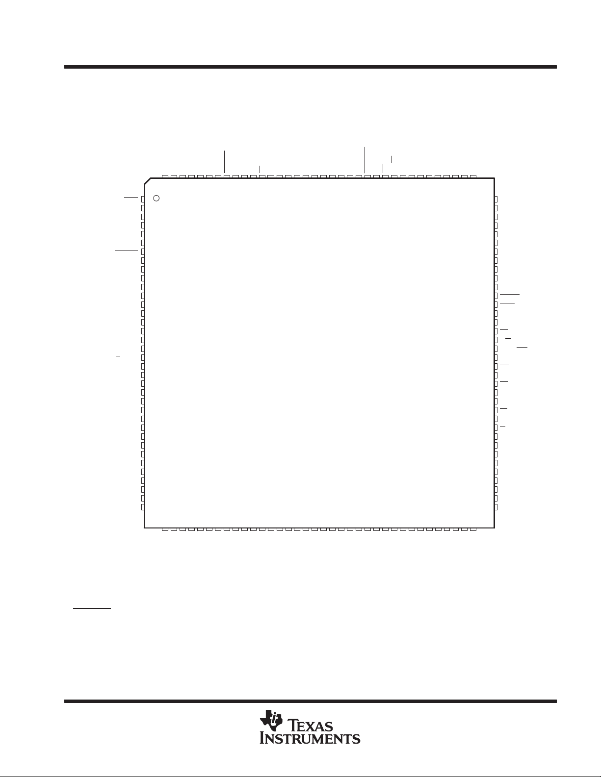
TMS320LF2407
PDPINTA
PLLF
TDIRA/
IOPB6
XINT2/ADCSOC/
IOPD0
CLKOUT
/IOPE0
PDPINTB
XTAL1/CLKIN
XTAL2
PLLV
CCA
PLLF2
BOOT_EN/XF
CCP
V
TP1
TP2
IOPF6
EMU0
EMU1/OFF
TCK
TDI
TDO
TMS
TMS2
TRST
DS
IS
PS
R/W
W/R
/IOPC0
RD
WE
STRB
READY
MP/MC
ENA_144
VIS_OE
A0
A1
A2
A3
A4
A5
A6
A7
A8
A9
A10
A11
A12
A13
A14
A15
D0
D1
D2
D3
D4
D5
D6
D7
D8
D9
D10
D11
D12
D13
D14
D15
PLLV
CCA
V
DD
DD
V
V
DD
DD
V
V
DDO
DDO
V
DDO
V
V
DDO
V
DDO
DDO
V
V
SS
SS
V
V
SS
SS
V
V
SSO
SSO
V
SSO
V
V
SSO
V
SSO
SSO
V
SSO
V
CAP1/QEP1/
IOPA3
CAP2/QEP2/
IOPA4
CAP3/
IOPA5
PWM1/
PWM2/
PWM3/
PWM4/
PWM5/
PWM6/
T1PWM/T1CMP/
IOPB4
T2PWM/T2CMP/
IOPB5
TCLKINA/
CAP4/QEP3/
IOPE7
CAP5/QEP4/
IOPF0
CAP6/
PWM7/
PWM8/
PWM9/
PWM10/
PWM11/
PWM12/
T3PWM/T3CMP/
IOPF2
T4PWM/T4CMP/
IOPF3
TDIRB/
IOPF4
TCLKINB/
ADCIN00
ADCIN01
ADCIN02
ADCIN03
ADCIN04
ADCIN05
ADCIN06
ADCIN07
ADCIN08
ADCIN09
ADCIN10
ADCIN11
ADCIN12
ADCIN13
ADCIN14
ADCIN15
REFHI
V
REFLO
V
CCA
V
SSA
V
CANRX/
CANTX/
SCITXD/
IOPA0
SCIRXD/
IOPA1
SPICLK/
IOPC4
SPISIMO/
IOPC2
SPISOMI/
IOPC3
SPISTE/
IOPC5
XINT1/
IOPA2
†
Bold, italicized pin names
indicate pin function after reset.
‡
BOOT_EN
is available only on flash devices.
IOPB7
IOPE6
IOPB3
IOPB2
IOPE5
IOPB1
IOPB0
IOPA7
IOPE4
IOPA6
IOPE3
IOPE2
IOPE1
IOPF1
IOPC7
IOPC6
IOPF5
IOPC1
BIO/
PGE PACKAGE
†
(TOP VIEW)
‡
ADVANCE
INFORMATION
TMS320LF2407, TMS320LF2406, TMS320LF2402
TMS320LC2406, TMS320LC2404, TMS320LC2402
DSP CONTROLLERS
SPRS094C – APRIL 1999 – REVISED OCTOBER 1999
6
POST OFFICE BOX 1443 • HOUSTON, TEXAS 77251–1443
SCIRXD/
TMS
TDO
V
DDO
V
SSO
TDI
PDPINTB
TCK
RS
IOPF6
V
DD
V
SS
TCLKINB/
IOPF5
XTAL2
XTAL1/CLKIN
BOOT_EN
/XF
§
BIO
/IOPC1
V
SSA
V
CCA
V
REFHI
V
REFLO
ADCIN08
ADCIN00
ADCIN09
ADCIN01
ADCIN10
TCLKINA/
IOPB7
PWM12/
IOPE6
PWM6/
IOPB3
V
SSO
V
DDO
PWM5/
IOPB2
PWM11/
IOPE5
PWM4/
IOPB1
V
SS
V
DD
PWM3/
IOPB0
PWM2/
IOPA7
PWM10/
IOPE4
PWM1/
IOPA6
V
CCP
PWM9/
IOPE3
TP1
PWM8/
IOPE2
TP2
PWM7/
IOPE1
V
SSO
V
DDO
CAP6/
IOPF1
CANRX/
IOPC7
‡
CANTX/
IOPC6
‡
50
49
48
47
46
45
44
43
42
41
40
39
38
37
36
35
34
33
32
31
30
29
28
27
26100
99
98
97
96
95
94
93
92
91
90
89
88
87
86
85
84
83
82
81
80
79
78
77
76
25242322212019181716151413121110987654321
51525354555657585960616263646566676869707172737475
ADCIN11
ADCIN02
ADCIN12
ADCIN03
ADCIN13
ADCIN04
ADCIN05
ADCIN14
ADCIN06
ADCIN07
ADCIN15
EMU1/
EMU0
CAP4/QEP3/
V
CAP1/QEP1/
CAP5/QEP4/
CAP2/QEP2/
V
CAP3/
/IOPE0
DD
DDO
TRST
TDIRB/
V
T4PWM/T4CMP/
PDPINTA
PLLF2
PLLF
T1PWM/T1CMP/
T2PWM/T2CMP/
XINT2/ADCSOC/
SCITXD/
SPISOMI/
SPISTE/
SPICLK/
DDO
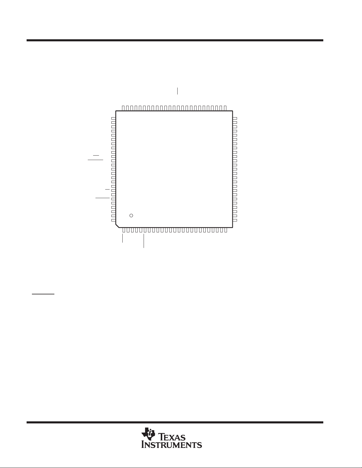
PZ PACKAGE
†
(TOP VIEW)
TDIRA/
TMS320LC2404
TMS320LC2406
TMS320LF2406
T3PWM/T3CMP/
XINT1/
PLLV
CCA
TMS2
V
DD
V
DDO
V
SS
V
SS
V
SSO
V
SSO
V
SSO
V
SSO
†
Bold, italicized pin names
indicate pin function after reset.
‡
CANTX and CANRX are not available on ’LC2404 devices.
§
BOOT_EN
is available only on flash devices.
IOPF4
IOPF3
IOPF2
IOPB6
IOPB4
IOPB5
IOPC0
IOPD0
IOPA2
IOPA0
IOPA1
SPISIMO/
IOPC2
IOPC3
IOPC5
IOPC4
IOPE7
CLKOUT
IOPA3
IOPF0
IOPA4
IOPA5
TDIRB/
IOPF4
OFF
ADVANCE
INFORMATION
TMS320LF2407, TMS320LF2406, TMS320LF2402
TMS320LC2406, TMS320LC2404, TMS320LC2402
DSP CONTROLLERS
SPRS094C – APRIL 1999 – REVISED OCTOBER 1999
7
POST OFFICE BOX 1443 • HOUSTON, TEXAS 77251–1443
V
REFHI
V
CCA
V
SSA
BOOT_EN
/XF
‡
XTAL1/CLKIN
XTAL2
V
SS
V
DD
RS
TCK
TDI
TDO
TMS
V
DDO
IOPC6
IOPC7
TP2
TP1
V
CCP
PWM1
PWM2
PWM3
V
DD
V
SS
PWM4
PWM5
V
ADCIN00
PDPINTA
PLLF2
PLLF
T1PWM/T1CMP/
T2PWM/T2CMP/
SCITXD/
EMU0
TMS2
TCLKINA/
PWM6/
CAP1/QEP1/
CAP2/QEP2/
CAP3/
CLKOUT
ADCIN01
ADCIN02
ADCIN03
ADCIN04
ADCIN05
ADCIN06
ADCIN07
REFLO
SCIRXD/
XINT2/ADCSOC/
PLLV
CCA
EMU1/
TRST
TMS320LC2402
TMS320LF2402
V
SSO
V
DDO
V
DDO
V
SSO
V
DD
V
SS
IOPB4
IOPB5
IOPD0
IOPA0
IOPA1
IOPC2
IOPC3
IOPC4
IOPB7
IOPB3
/IOPE0
IOPA5
IOPA4
IOPA3
OFF
191 2 3 4 5 6 7 8 9101112131415161718
3351 343550 49 48 47 46 45 44 43 42 41 40 3938 37 36
52
64
53
54
55
56
57
58
59
60
61
62
63
32
20
31
30
29
28
27
26
25
24
23
22
21
PG PACKAGE
†
(TOP VIEW)
†
Bold, italicized pin names
indicate pin function after reset.
‡
BOOT_EN
is available only on flash devices.
V
SSO
ADVANCE
INFORMATION

TMS320LF2407, TMS320LF2406, TMS320LF2402
TMS320LC2406, TMS320LC2404, TMS320LC2402
DSP CONTROLLERS
SPRS094C – APRIL 1999 – REVISED OCTOBER 1999
8
POST OFFICE BOX 1443 • HOUSTON, TEXAS 77251–1443
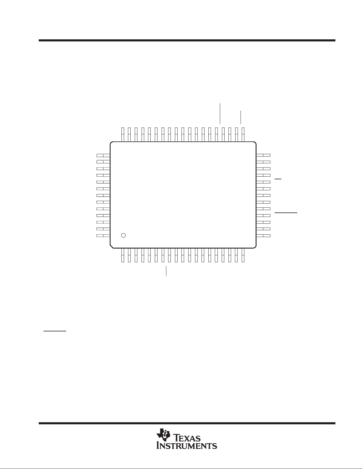
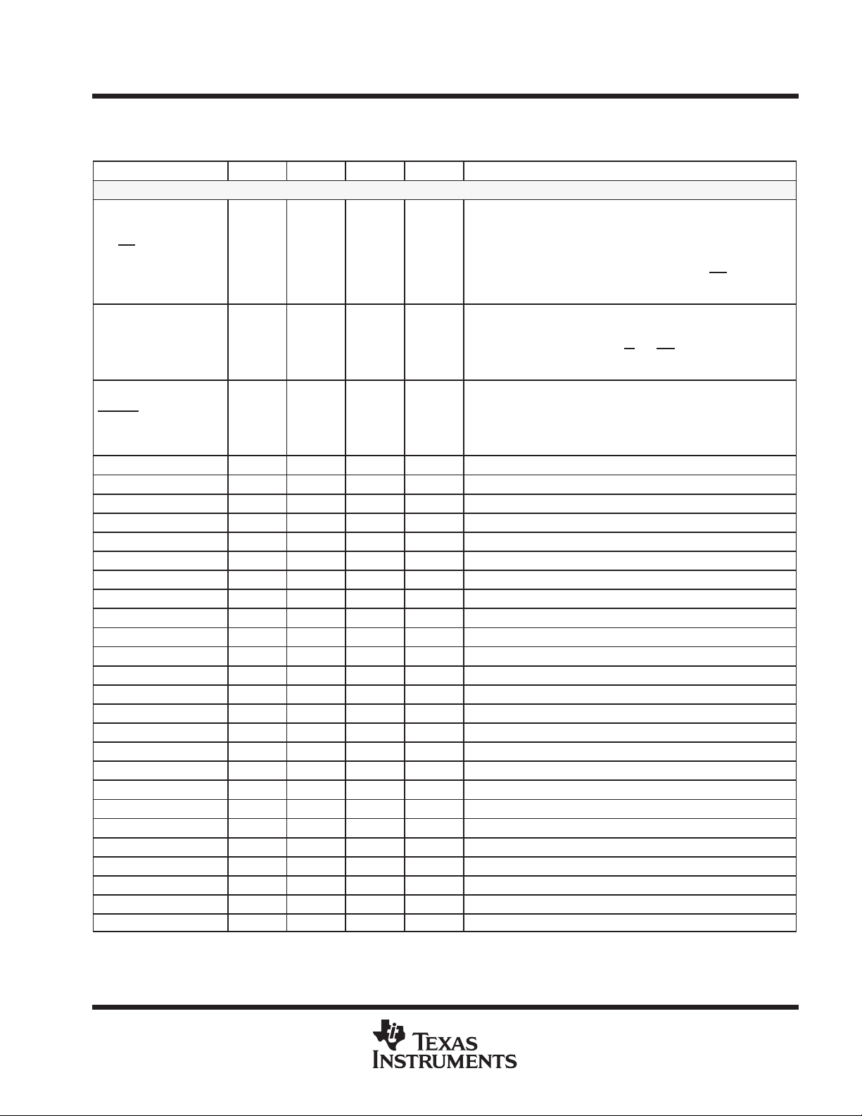
pin functions
The TMS320LF2407 device is the superset of all the ’240x devices. All signals are available on the ’2407 device.
Table 2 lists the key signals available in the ’240x family of devices.
Table 2. ’LF240x and ’LC240x Pin List and Package Options
†‡
PIN NAME ’LF2407 ’2406 ’LC2404 ’2402 DESCRIPTION
EVENT MANAGER A (EVA)
CAP1/QEP1/
IOPA3
83 57 57 4
Capture input #1/quadrature encoder pulse input #1 (EVA) or
GPIO (↑)
CAP2/QEP2/
IOPA4
79 55 55 3
Capture input #2/quadrature encoder pulse input #2 (EVA) or
GPIO (↑)
CAP3/
IOPA5
75 52 52 2 Capture input #3 (EVA) or GPIO (↑)
PWM1/
IOPA6
56 39 39 59
§
Compare/PWM output pin #1 (EVA) or GPIO (↑)
PWM2/
IOPA7
54 37 37 58
§
Compare/PWM output pin #2 (EVA) or GPIO (↑)
PWM3/
IOPB0
52 36 36 57
§
Compare/PWM output pin #3 (EVA) or GPIO (↑)
PWM4/
IOPB1
47 33 33 54
§
Compare/PWM output pin #4 (EVA) or GPIO (↑)
PWM5/
IOPB2
44 31 31 53
§
Compare/PWM output pin #5 (EVA) or GPIO (↑)
PWM6/
IOPB3
40 28 28 50 Compare/PWM output pin #6 (EVA) or GPIO (↑)
T1PWM/T1CMP/
IOPB4
16 12 12 40 Timer 1 compare output (EVA) or GPIO (↑)
T2PWM/T2CMP/
IOPB5
18 13 13 41 Timer 2 compare output (EVA) or GPIO (↑)
TDIRA/
IOPB6
14 11 11
Counting direction for general-purpose (GP) timer (EVA) or
GPIO. If TDIRA=1, upward counting is selected. If TDIRA=0,
downward counting is selected. (↑)
TCLKINA/
IOPB7
37 26 26 49
External clock input for GP timer (EVA) or GPIO. Note that timer
can also use the internal device clock. (↑)
EVENT MANAGER B (EVB)
CAP4/QEP3/
IOPE7
88 60 60
Capture input #4/quadrature encoder pulse input #3 (EVB) or
GPIO (↑)
CAP5/QEP4/
IOPF0
81 56 56
Capture input #5/quadrature encoder pulse input #4 (EVB) or
GPIO (↑)
CAP6/
IOPF1
69 48 48 Capture input #6 (EVB) or GPIO (↑)
PWM7/
IOPE1
65 45 45 Compare/PWM output pin #7 (EVB) or GPIO (↑)
PWM8/
IOPE2
62 43 43 Compare/PWM output pin #8 (EVB) or GPIO (↑)
PWM9/
IOPE3
59 41 41 Compare/PWM output pin #9 (EVB) or GPIO (↑)
PWM10/
IOPE4
55 38 38 Compare/PWM output pin #10 (EVB) or GPIO (↑)
PWM11/
IOPE5
46 32 32 Compare/PWM output pin #11 (EVB) or GPIO (↑)
PWM12/
IOPE6
38 27 27 Compare/PWM output pin #12 (EVB) or GPIO (↑)
T3PWM/T3CMP/
IOPF2
8 7 7 Timer 3 compare output (EVB) or GPIO (↑)
T4PWM/T4CMP/
IOPF3
6 5 5 Timer 4 compare output (EVB) or GPIO (↑)
TDIRB/
IOPF4
2 2 2
Counting direction for general-purpose (GP) timer (EVB) or
GPIO. If TDIRB=1, upward counting is selected. If TDIRB=0,
downward counting is selected. (↑)
TCLKINB/
IOPF5
126 89 89
External clock input for GP timer (EVB) or GPIO. Note that timer
can also use the internal device clock. (↑)
†
Bold, italicized pin names
indicate pin function after reset.
‡
GPIO – General-purpose input/output pin. All GPIOs come up as input after reset.
§
Pin changes with respect to SPRS094B data sheet.
LEGEND: ↑ – Internal pullup ↓ – Internal pulldown
ADVANCE
INFORMATION
TMS320LF2407, TMS320LF2406, TMS320LF2402
TMS320LC2406, TMS320LC2404, TMS320LC2402
DSP CONTROLLERS
SPRS094C – APRIL 1999 – REVISED OCTOBER 1999
9
POST OFFICE BOX 1443 • HOUSTON, TEXAS 77251–1443
pin functions (continued)
Table 2. ’LF240x and ’LC240x Pin List and Package Options
†‡
(Continued)
PIN NAME ’LF2407 ’2406 ’LC2404 ’2402 DESCRIPTION
ANALOG-TO-DIGITAL CONVERTER (ADC)
ADCIN00 112 79 79 18 Analog input #0 to the ADC
ADCIN01 110 77 77 17 Analog input #1 to the ADC
ADCIN02 107 74 74 16 Analog input #2 to the ADC
ADCIN03 105 72 72 15 Analog input #3 to the ADC
ADCIN04 103 70 70 14 Analog input #4 to the ADC
ADCIN05 102 69 69 13 Analog input #5 to the ADC
ADCIN06 100 67 67 12 Analog input #6 to the ADC
ADCIN07 99 66 66 11 Analog input #7 to the ADC
ADCIN08 113 80 80 Analog input #8 to the ADC
ADCIN09 111 78 78 Analog input #9 to the ADC
ADCIN10 109 76 76 Analog input #10 to the ADC
ADCIN11 108 75 75 Analog input #11 to the ADC
ADCIN12 106 73 73 Analog input #12 to the ADC
ADCIN13 104 71 71 Analog input #13 to the ADC
ADCIN14 101 68 68 Analog input #14 to the ADC
ADCIN15 98 65 65 Analog input #15 to the ADC
V
REFHI
115 82 82 20 ADC analog high-voltage reference input
V
REFLO
114 81 81 19 ADC analog low-voltage reference input
V
CCA
116 83 83 21
Analog supply voltage for ADC (3.3 V). V
CCA
must
be isolated from digital supply voltage.
V
SSA
117 84 84 22 Analog ground reference for ADC
CONTROLLER AREA NETWORK (CAN), SERIAL COMMUNICATIONS INTERFACE (SCI), SERIAL PERIPHERAL INTERFACE (SPI)
CANRX 70 49 – –
CANRX/
IOPC7
IOPC7 70 49 49 63
CAN receive data or GPIO (↑)
CANTX 72 50 – –
CANTX/
IOPC6
IOPC6 72 50 50 64
CAN transmit data or GPIO (↑)
SCITXD/
IOPA0
25 17 17 43
SCI asynchronous serial port transmit data or
GPIO (↑)
SCIRXD/
IOPA1
26 18 18 44
SCI asynchronous serial port receive data or or
GPIO (↑)
SPICLK 35 24 24 –
SPICLK/
IOPC4
IOPC4 35 24 24 47
SPI clock or GPIO (↑)
SPISIMO 30 21 21 –
SPISIMO/
IOPC2
IOPC2 30 21 21 45
SPI slave in, master out or GPIO (↑)
SPISOMI 32 22 22 –
SPISOMI/
IOPC3
IOPC3 32 22 22 46
SPI slave out, master in or GPIO (↑)
SPISTE 33 23 23 –
SPISTE/
IOPC5
IOPC5 33 23 23 –
SPI slave transmit enable (optional) or GPIO (↑)
†
Bold, italicized pin names
indicate pin function after reset.
‡
GPIO – General-purpose input/output pin. All GPIOs come up as input after reset.
LEGEND: ↑ – Internal pullup ↓ – Internal pulldown
ADVANCE
INFORMATION
TMS320LF2407, TMS320LF2406, TMS320LF2402
TMS320LC2406, TMS320LC2404, TMS320LC2402
DSP CONTROLLERS
SPRS094C – APRIL 1999 – REVISED OCTOBER 1999
10
POST OFFICE BOX 1443 • HOUSTON, TEXAS 77251–1443
pin functions (continued)
Table 2. ’LF240x and ’LC240x Pin List and Package Options
†‡
(Continued)
PIN NAME ’LF2407 ’2406 ’LC2404 ’2402 DESCRIPTION
EXTERNAL INTERRUPTS, CLOCK
RS 133 93 93 28
Device reset. RS causes the ’240x to terminate
execution and sets PC = 0. When RS
is brought to a
high level, execution begins at location zero of
program memory. RS
affects (or sets to zero) various
registers and status bits. When the watchdog timer
overflows, it initiates a system reset pulse that is
reflected on the RS
pin. (↑)
PDPINTA 7 6 6 36
Power drive protection interrupt input. This interrupt,
when activated, puts the PWM output pins (EVA) in the
high-impedance state should motor drive/power
converter abnormalities, such as overvoltage or
overcurrent, etc., arise. PDPINTA
is a
falling-edge-sensitive interrupt. (↑)
XINT1/
IOPA2
23 16 16
External user interrupt 1 or GPIO. Both XINT1 and
XINT2 are edge-sensitive. The edge polarity is
programmable. (↑)
XINT2/ADCSOC/
IOPD0
21 15 15 42
External user interrupt 2 and ADC start of conversion
or GPIO. External “start-of-conversion” input for
ADC/GPIO. Both XINT1 and XINT2 are
edge-sensitive. The edge polarity is
programmable. (↑)
CLKOUT
/IOPE0 73 51 51 1
Clock output or GPIO. This pin outputs either the CPU
clock (CLKOUT) or the watchdog clock (WDCLK). The
selection is made by the CLKSRC bit (bit 14) of the
System Control and Status Register (SCSR). This pin
can be used as a GPIO if not used as a clock output
pin. (↑)
PDPINTB 137 95 95
Power drive protection interrupt input. This interrupt,
when activated, puts the PWM output pins (EVB) in
the high-impedance state should motor drive/power
converter abnormalities, such as overvoltage or
overcurrent, etc., arise. PDPINT
is a
falling-edge-sensitive interrupt. (↑)
OSCILLATOR, PLL, FLASH, BOOT, AND MISCELLANEOUS
XTAL1/CLKIN 123 87 87 24
PLL oscillator input pin. Crystal input to PLL/clock
source input to PLL. XTAL1/CLKIN is tied to one side
of a reference crystal.
XTAL2 124 88 88 25
Crystal output. PLL oscillator output pin. XTAL2 is tied
to one side of a reference crystal. This pin goes in the
high-impedance state when EMU1/OFF
is active low.
PLLF 11 9 9 38 Filter input 1
PLLV
CCA
12 10 10 39 PLL supply (3.3 V)
PLLF2 10 8 8 37 Filter input 2
BOOT_EN 121 86 – 23
Boot ROM enable, GPO, XF. This pin will be sampled
as input (BOOT_EN
) to update SCSR2.3 (BOOT_EN
BOOT_EN / XF
XF 121 86 86 23
bit) during reset and then driven as an output signal for
XF. ROM devices do not have boot ROM, hence, no
BOOT_EN modes. (↑)
†
Bold, italicized pin names
indicate pin function after reset.
‡
GPIO – General-purpose input/output pin. All GPIOs come up as input after reset.
LEGEND: ↑ – Internal pullup ↓ – Internal pulldown
ADVANCE
INFORMATION
TMS320LF2407, TMS320LF2406, TMS320LF2402
TMS320LC2406, TMS320LC2404, TMS320LC2402
DSP CONTROLLERS
SPRS094C – APRIL 1999 – REVISED OCTOBER 1999
11
POST OFFICE BOX 1443 • HOUSTON, TEXAS 77251–1443
pin functions (continued)
Table 2. ’LF240x and ’LC240x Pin List and Package Options
†‡
(Continued)
PIN NAME ’LF2407 ’2406 ’LC2404 ’2402 DESCRIPTION
OSCILLATOR, PLL, FLASH, BOOT, AND MISCELLANEOUS (CONTINUED)
V
CCP
(5V) 58 40 40 60
§
Flash programming voltage pin. This is the 5-V supply used for
flash programming. Flash cannot be programmed if this pin is
held at 0 V . Connect to 5-V supply for programming or tie it to
GND during functional mode.
TP1 (Flash) 60 42 42 61
§
Flash array test pin.
Do not connect.
TP2 (Flash) 63 44 44 62
§
Flash array test pin
. Do not connect.
IOPF6 131 92 92 General-purpose I/O (↑)
BIO
/IOPC1 119 85 85
Branch control input. BIO is polled by the BCND pma,BIO
instruction. If BIO
is low, a branch is executed. If BIO is not
used, it should be pulled high. This pin is configured as a branch
control input by all device resets. It can be used as a GPIO, if
not used as a branch control input. (↑)
EMULATION AND TEST
EMU0 90 61 61 7
Emulator I/O #0 with internal pullup. When TRST is driven high,
this pin is used as an interrupt to or from the emulator system
and is defined as input/output through the JTAG scan. (↑)
EMU1/OFF 91 62 62 8
Emulator pin 1. Emulator pin 1 disables all outputs. When TRST
is driven high, EMU1/OFF is used as an interrupt to or from the
emulator system and is defined as an input/output through the
JTAG scan. When TRST
is driven low, this pin is configured as
OFF
. EMU1/OFF, when active low, puts all output drivers in the
high-impedance state. Note that OFF
is used exclusively for
testing and emulation purposes (not for multiprocessing
applications). Therefore, for the OFF
condition, the following
apply:
TRST
= 0
EMU0 = 1
EMU1/OFF
= 0
TCK 135 94 94 29 JTAG test clock with internal pullup (↑)
TDI 139 96 96 30
JTAG test data input (TDI) with internal pullup. TDI is clocked
into the selected register (instruction or data) on a rising edge of
TCK. (↑)
TDO 142 99 99 31
JTAG scan out, test data output (TDO). The contents of the
selected register (instruction or data) is shifted out of TDO on
the falling edge of TCK. (↓)
TMS 144 100 100 32
JTAG test-mode select (TMS) with internal pullup. This serial
control input is clocked into the TAP controller on the rising edge
of TCK. (↑)
TMS2 36 25 25 48
JTAG test-mode select 2 (TMS) with internal pullup. This serial
control input is clocked into the TAP controller on the rising edge
of TCK. Used for test and emulation only. (↑)
TRST 1 1 1 33
JTAG test reset with internal pulldown. TRST, when driven high,
gives the scan system control of the operations of the device. If
this signal is not connected or driven low, the device operates in
its functional mode, and the test reset signals are ignored. (↓)
†
Bold, italicized pin names
indicate pin function after reset.
‡
GPIO – General-purpose input/output pin. All GPIOs come up as input after reset.
§
Pin changes with respect to SPRS094B data sheet.
LEGEND: ↑ – Internal pullup ↓ – Internal pulldown
ADVANCE
INFORMATION
TMS320LF2407, TMS320LF2406, TMS320LF2402
TMS320LC2406, TMS320LC2404, TMS320LC2402
DSP CONTROLLERS
SPRS094C – APRIL 1999 – REVISED OCTOBER 1999
12
POST OFFICE BOX 1443 • HOUSTON, TEXAS 77251–1443
pin functions (continued)
Table 2. ’LF240x and ’LC240x Pin List and Package Options
†‡
(Continued)
PIN NAME ’LF2407 ’2406 ’LC2404 ’2402 DESCRIPTION
ADDRESS, DATA, AND MEMORY CONTROL SIGNALS
DS 87
Data space strobe. IS, DS, and PS are always high
unless low-level asserted for access to the relevant
external memory space or I/O. They are placed in the
high-impedance state during reset, power down, and
when EMU1/OFF
is active low.
IS 82
I/O space strobe. IS, DS, and PS are always high
unless low-level asserted for access to the relevant
external memory space or I/O. They are placed in the
high-impedance state during reset, power down, and
when EMU1/OFF
is active low.
PS 84
Program space strobe. IS, DS, and PS are always
high unless low-level asserted for access to the
relevant external memory space or I/O. They are
placed in the high-impedance state during reset,
power down, and when EMU1/OFF
is active low.
R/W 92
Read/write qualifier signal. R/W indicates transfer
direction during communication to an external device.
It is normally in read mode (high), unless low level is
asserted for performing a write operation. It is placed
in the high-impedance state when EMU1/OFF
is
active low and during power down.
W/R
19
Write/Read qualifier or GPIO. This is an inverted R/W
signal useful for zero-wait-state memory interface. It
W/R
/ IOPC0
IOPC0 19 14 14
is normally low, unless a memory write operation is
performed. See T able 13, Port C section, for reset
note regarding ’LF2406 and ’LF2402. (↑)
RD 93
Read enable strobe. Read-select indicates an active,
external read cycle. RD
is active on all external
program, data, and I/O reads. RD
goes into the
high-impedance state when EMU1/OFF
is active low.
WE 89
Write enable strobe. The falling edge of WE indicates
that the device is driving the external data bus
(D15–D0). WE
is active on all external program,
data, and I/O writes. WE
goes in the high-impedance
state when EMU1/OFF
is active low.
STRB 96
External memory access strobe. STRB is always high
unless asserted low to indicate an external bus cycle.
STRB
is active for all off-chip accesses. It is placed in
the high-impedance state during power down, and
when EMU1/OFF
is active low.
READY 120
READY is pulled low to add wait states for external
accesses. READY indicates that an external device is
prepared for a bus transaction to be completed. If the
device is not ready, it pulls the READY pin low. The
processor waits one cycle and checks READY again.
Note that the processor performs READY-detection if
at least one software wait state is programmed. To
meet the external READY timings, the wait-state
generator control register (WSGR) should be
programmed for at least one wait state. (↑)
†
Bold, italicized pin names
indicate pin function after reset.
‡
GPIO – General-purpose input/output pin. All GPIOs come up as input after reset.
LEGEND: ↑ – Internal pullup ↓ – Internal pulldown
ADVANCE
INFORMATION
TMS320LF2407, TMS320LF2406, TMS320LF2402
TMS320LC2406, TMS320LC2404, TMS320LC2402
DSP CONTROLLERS
SPRS094C – APRIL 1999 – REVISED OCTOBER 1999
13
POST OFFICE BOX 1443 • HOUSTON, TEXAS 77251–1443
pin functions (continued)
Table 2. ’LF240x and ’LC240x Pin List and Package Options
†‡
(Continued)
PIN NAME ’LF2407 ’2406 ’LC2404 ’2402 DESCRIPTION
ADDRESS, DATA, AND MEMORY CONTROL SIGNALS (CONTINUED)
MP/MC 118
Microprocessor/Microcomputer mode select. If this pin is low
during reset, the device is put in microcomputer mode and
program execution begins at 0000h of internal program memory
(flash EEPROM). A high value during reset puts the device in
microprocessor mode and program execution begins at 0000h of
external program memory. This line sets the MP/MC
bit (bit 2 in
the SCSR2 register). (↓)
ENA_144 122
Active high to enable external interface signals. If pulled low, the
’2407 behaves like the ’2406/’2404—i.e., it has no external
memory and generates an illegal address if any of the three
external spaces are accessed (IS
and DS asserted). This pin
has an internal pulldown. (↓)
VIS_OE 97
Visibility output enable (active when data bus is output). This pin
is active (low) whenever the external databus is driving as an
output during visibility mode. Can be used by external decode
logic to prevent data bus contention while running in visibility
mode.
A0 80 Bit 0 of the 16-bit address bus
A1 78 Bit 1 of the 16-bit address bus
A2 74 Bit 2 of the 16-bit address bus
A3 71 Bit 3 of the 16-bit address bus
A4 68 Bit 4 of the 16-bit address bus
A5 64 Bit 5 of the 16-bit address bus
A6 61 Bit 6 of the 16-bit address bus
A7 57 Bit 7 of the 16-bit address bus
A8 53 Bit 8 of the 16-bit address bus
A9 51 Bit 9 of the 16-bit address bus
A10 48 Bit 10 of the 16-bit address bus
A11 45 Bit 11 of the 16-bit address bus
A12 43 Bit 12 of the 16-bit address bus
A13 39 Bit 13 of the 16-bit address bus
A14 34 Bit 14 of the 16-bit address bus
A15 31 Bit 15 of the 16-bit address bus
D0 127 Bit 0 of 16-bit data bus (↑)
D1 130 Bit 1 of 16-bit data bus (↑)
D2 132 Bit 2 of 16-bit data bus (↑)
D3 134 Bit 3 of 16-bit data bus (↑)
D4 136 Bit 4 of 16-bit data bus (↑)
D5 138 Bit 5 of 16-bit data bus (↑)
D6 143 Bit 6 of 16-bit data bus (↑)
D7 5 Bit 7 of 16-bit data bus (↑)
D8 9 Bit 8 of 16-bit data bus (↑)
†
Bold, italicized pin names
indicate pin function after reset.
‡
GPIO – General-purpose input/output pin. All GPIOs come up as input after reset.
LEGEND: ↑ – Internal pullup ↓ – Internal pulldown
ADVANCE
INFORMATION
TMS320LF2407, TMS320LF2406, TMS320LF2402
TMS320LC2406, TMS320LC2404, TMS320LC2402
DSP CONTROLLERS
SPRS094C – APRIL 1999 – REVISED OCTOBER 1999
14
POST OFFICE BOX 1443 • HOUSTON, TEXAS 77251–1443
pin functions (continued)
Table 2. ’LF240x and ’LC240x Pin List and Package Options
†‡
(Continued)
PIN NAME ’LF2407 ’2406 ’LC2404 ’2402 DESCRIPTION
ADDRESS, DATA, AND MEMORY CONTROL SIGNALS (CONTINUED)
D9 13 Bit 9 of 16-bit data bus (↑)
D10 15 Bit 10 of 16-bit data bus (↑)
D11 17 Bit 11 of 16-bit data bus (↑)
D12 20 Bit 12 of 16-bit data bus (↑)
D13 22 Bit 13 of 16-bit data bus (↑)
D14 24 Bit 14 of 16-bit data bus (↑)
D15 27 Bit 15 of 16-bit data bus (↑)
POWER SUPPLY
29 20 20 6
50 35 35 27
V
DD
86 59 59 56
§
Core supply +3.3 V . Digital logic supply voltage.
129 91 91
4 4 4 10
42 30 30 35
67 47 47 52
§
V
DDO
77 54 54
I/O buffer supply +3.3 V. Digital logic and buffer supply voltage.
95 64 64
141 98 98
28 19 19 5
49 34 34 26
V
SS
85 58 58 55
§
Core ground. Digital logic ground reference.
128 90 90
3 3 3 9
41 29 29 34
66 46 46 51
§
V
SSO
76 53 53
I/O buffer ground. Digital logic and buffer ground reference.
V
SSO
94 63 63
I/O
buffer
ground.
Digital
logic
and
buffer
ground
reference.
125 97 97
140
†
Bold, italicized pin names
indicate pin function after reset.
‡
GPIO – General-purpose input/output pin. All GPIOs come up as input after reset.
§
Pin changes with respect to SPRS094B data sheet.
LEGEND: ↑ – Internal pullup ↓ – Internal pulldown
ADVANCE
INFORMATION

TMS320LF2407, TMS320LF2406, TMS320LF2402
TMS320LC2406, TMS320LC2404, TMS320LC2402
DSP CONTROLLERS
SPRS094C – APRIL 1999 – REVISED OCTOBER 1999
15
POST OFFICE BOX 1443 • HOUSTON, TEXAS 77251–1443
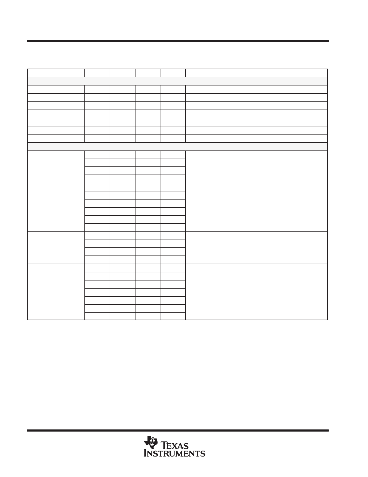
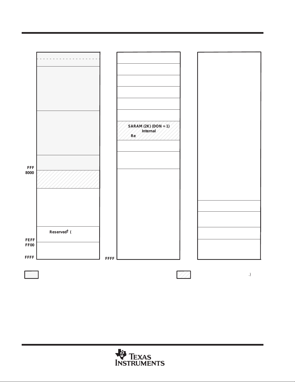
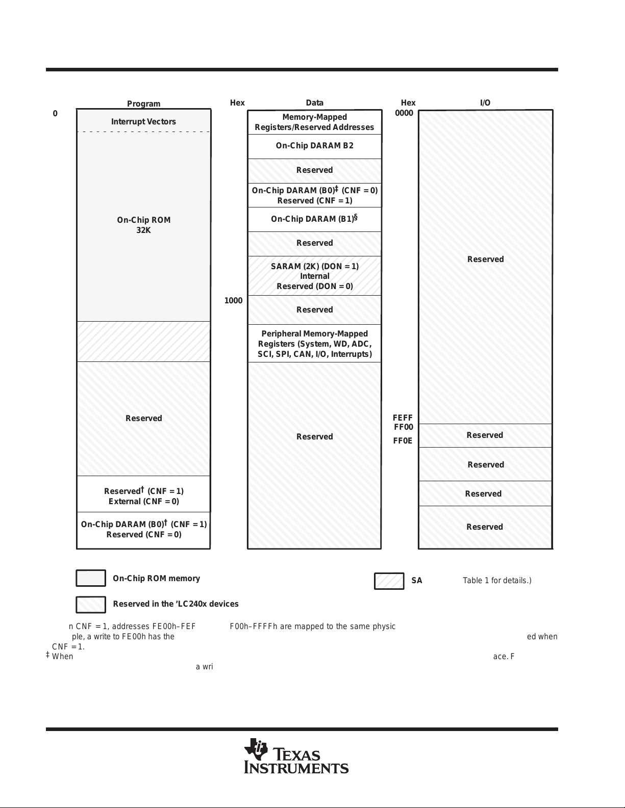
memory maps – ’LF2407
Reserved
0000
003F
Hex Program
Interrupt Vectors
On-Chip Flash Memory (Sectored) – if MP/MC = 0
External Program Memory – if MP/MC
= 1
7FFF
8000
0000
005F
0060
Hex Data
Memory-Mapped
Registers/Reserved Addresses
007F
0080
On-Chip DARAM B2
01FF
Reserved
02FF
0300
On-Chip DARAM (B0)
‡
(CNF = 0)
Reserved (CNF = 1)
03FF
0400
On-Chip DARAM (B1)
§
07FF
0800
Reserved
6FFF
7000
Reserved
Peripheral Memory-Mapped
Registers (System, WD, ADC,
SCI, SPI, CAN, I/O, Interrupts)
7FFF
8000
External
0000
Hex I/O
FEFF
FF00
FF0E
FF0F
Reserved
External
FFFF
FEFF
FF00
Reserved
†
(CNF = 1)
External (CNF = 0)
FDFF
FE00
External
On-Chip DARAM (B0)
†
(CNF = 1)
External (CNF = 0)
FFFF
FFFE
Wait-State Generator Control
Register (On-Chip)
FF10
Flash Control Mode Register
(Only for Flash Devices)
SARAM (See Table 1 for details.)
FFFF
SARAM (2K) (PON = 1)
Internal
External (PON=0)
87FF
8800
0FFF
FLASH SECTOR 0 (4K)
1000
3FFF
FLASH SECTOR 1 (12K)
FLASH SECTOR 2 (12K)
FLASH SECTOR 3 (4K)
4000
6FFF
7000
0FFF
1000
0200
SARAM (2K) (DON = 1)
Internal
External (DON=0)
0040
NOTE A: Boot ROM: If the boot ROM is enabled, then address 0000–00FF in the program space will be occupied by boot ROM.
†
When CNF = 1, addresses FE00h–FEFFh and FF00h–FFFFh are mapped to the same physical block (B0) in program-memory space. For
example, a write to FE00h has the same effect as a write to FF00h. For simplicity, addresses FE00h–FEFFh are referred to as reserved when
CNF = 1.
‡
When CNF = 0, addresses 0100h–01FFh and 0200h–02FFh are mapped to the same physical block (B0) in data-memory space. For example,
a write to 0100h has the same effect as a write to 0200h. For simplicity , addresses 0100h–01FFh are referred to as reserved.
§
Addresses 0300h–03FFh and 0400h–04FFh are mapped to the same physical block (B1) in data-memory space. For example, a write to 0400h
has the same effect as a write to 0300h. For simplicity , addresses 0400h–04FFh are referred to as reserved.
Figure 1. TMS320LF2407 Memory Map
ADVANCE
INFORMATION
TMS320LF2407, TMS320LF2406, TMS320LF2402
TMS320LC2406, TMS320LC2404, TMS320LC2402
DSP CONTROLLERS
SPRS094C – APRIL 1999 – REVISED OCTOBER 1999
16
POST OFFICE BOX 1443 • HOUSTON, TEXAS 77251–1443
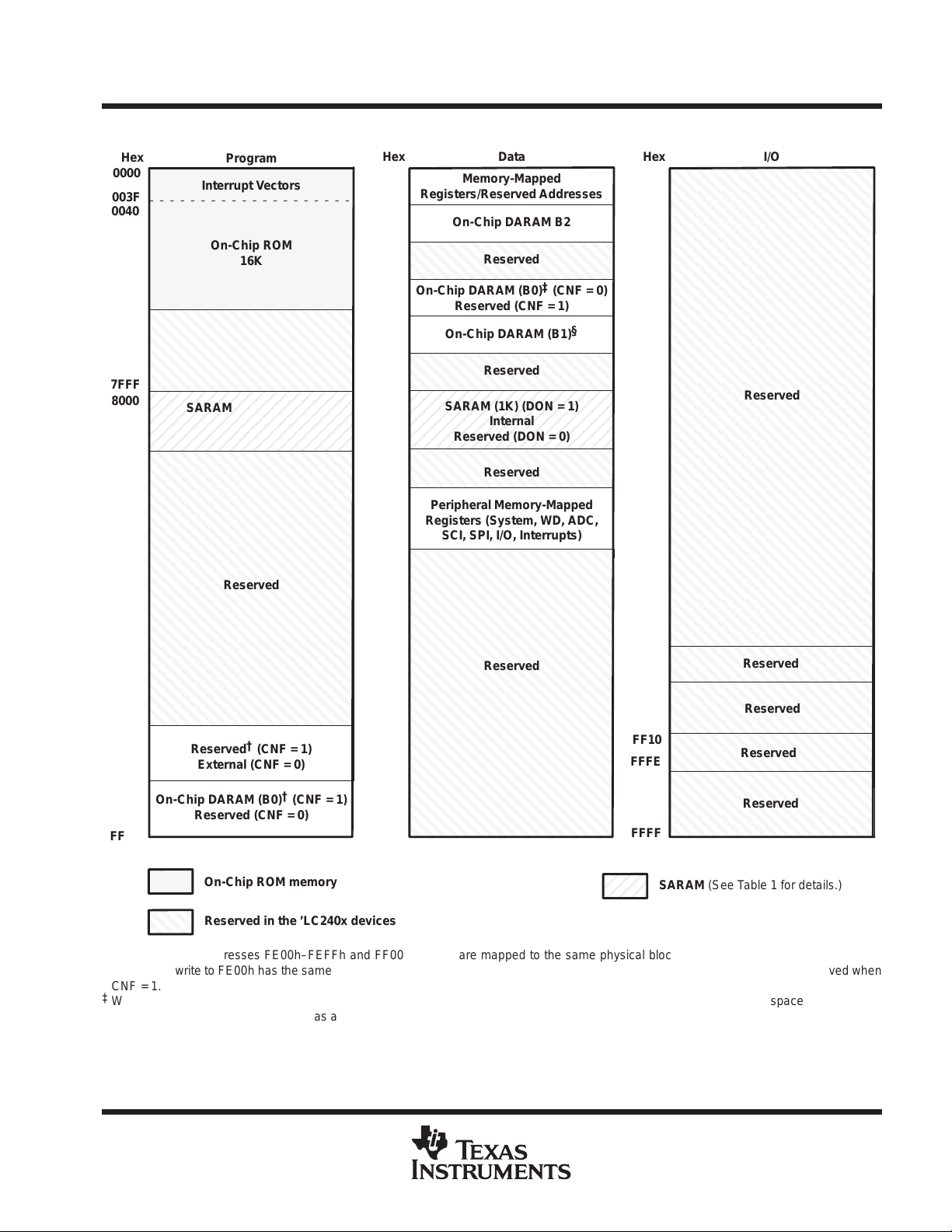
memory maps (continued) – ’LF2406
Reserved
On-Chip Flash Memory (Sectored)
0000
005F
0060
Hex Data
Memory-Mapped
Registers/Reserved Addresses
007F
0080
On-Chip DARAM B2
01FF
0200
Reserved
02FF
0300
On-Chip DARAM (B0)
‡
(CNF = 0)
Reserved (CNF = 1)
03FF
0400
On-Chip DARAM (B1)
§
07FF
0800
Reserved
SARAM (2K) (DON = 1)
Internal
Reserved (DON = 0)
6FFF
7000
Reserved
Peripheral Memory-Mapped
Registers (System, WD, ADC,
SCI, SPI, CAN, I/O, Interrupts)
7FFF
8000
Reserved
0000
Hex I/O
FEFF
FF00
FF0E
FF0F
Reserved
Reserved
FFFF
FFFE
Reserved
FF10
Flash Control Mode Register
(Only for Flash devices)
SARAM (See Table 1 for details.)
FFFF
0FFF
1000
0000
003F
Hex Program
Interrupt Vectors
7FFF
8000
FFFF
FEFF
FF00
Reserved
†
(CNF = 1)
External (CNF = 0)
FDFF
FE00
On-Chip DARAM (B0)
†
(CNF = 1)
External (CNF = 0)
SARAM (2K) (PON = 1)
Internal
External (PON=0)
87FF
8800
0FFF
FLASH SECTOR 0 (4K)
1000
3FFF
FLASH SECTOR 1 (12K)
FLASH SECTOR 2 (12K)
FLASH SECTOR 3 (4K)
4000
6FFF
7000
Reserved
0040
NOTE A: Boot ROM: If the boot ROM is enabled, then address 0000–00FF in the program space will be occupied by boot ROM.
†
When CNF = 1, addresses FE00h–FEFFh and FF00h–FFFFh are mapped to the same physical block (B0) in program-memory space. For
example, a write to FE00h has the same effect as a write to FF00h. For simplicity, addresses FE00h–FEFFh are referred to as reserved when
CNF = 1.
‡
When CNF = 0, addresses 0100h–01FFh and 0200h–02FFh are mapped to the same physical block (B0) in data-memory space. For example,
a write to 0100h has the same effect as a write to 0200h. For simplicity , addresses 0100h–01FFh are referred to as reserved.
§
Addresses 0300h–03FFh and 0400h–04FFh are mapped to the same physical block (B1) in data-memory space. For example, a write to 0400h
has the same effect as a write to 0300h. For simplicity , addresses 0400h–04FFh are referred to as reserved.
Figure 2. TMS320LF2406 Memory Map
ADVANCE
INFORMATION
TMS320LF2407, TMS320LF2406, TMS320LF2402
TMS320LC2406, TMS320LC2404, TMS320LC2402
DSP CONTROLLERS
SPRS094C – APRIL 1999 – REVISED OCTOBER 1999
17
POST OFFICE BOX 1443 • HOUSTON, TEXAS 77251–1443
memory maps (continued) – ’LF2402
Reserved
On-Chip Flash Memory (Sectored)
0000
005F
0060
Hex Data
Memory-Mapped
Registers/Reserved Addresses
007F
0080
On-Chip DARAM B2
01FF
0200
Reserved
02FF
0300
On-Chip DARAM (B0)
‡
(CNF = 0)
Reserved (CNF = 1)
03FF
0400
On-Chip DARAM (B1)
§
07FF
0800
Reserved
6FFF
7000
Reserved
Peripheral Memory-Mapped
Registers (System, WD, ADC,
SCI, I/O, Interrupts)
7FFF
8000
Reserved
0000
Hex I/O
FEFF
FF00
FF0E
FF0F
Reserved
Reserved
FFFF
FFFE
FF10
Flash Control Mode Register
(Only for Flash devices)
FFFF
0FFF
1000
Reserved
Reserved
0000
Hex Program
Interrupt Vectors
FFFF
FEFF
FF00
Reserved
†
(CNF = 1)
External (CNF = 0)
FDFF
FE00
On-Chip DARAM (B0)
†
(CNF = 1)
External (CNF = 0)
0FFF
003F
Hex Program
7FFF
8000
FFFF
FEFF
FF00
Reserved
†
(CNF = 1)
External (CNF = 0)
FDFF
FE00
Reserved
FLASH SECTOR 0 (4K)
FLASH SECTOR 1 (4K)
Reserved
87FF
8800
2000
Reserved
1000
1FFF
0040
NOTE A: Boot ROM: If the boot ROM is enabled, then address 0000–00FF in the program space will be occupied by boot ROM.
†
When CNF = 1, addresses FE00h–FEFFh and FF00h–FFFFh are mapped to the same physical block (B0) in program-memory space. For
example, a write to FE00h has the same effect as a write to FF00h. For simplicity, addresses FE00h–FEFFh are referred to as reserved when
CNF = 1.
‡
When CNF = 0, addresses 0100h–01FFh and 0200h–02FFh are mapped to the same physical block (B0) in data-memory space. For example,
a write to 0100h has the same effect as a write to 0200h. For simplicity , addresses 0100h–01FFh are referred to as reserved.
§
Addresses 0300h–03FFh and 0400h–04FFh are mapped to the same physical block (B1) in data-memory space. For example, a write to 0400h
has the same effect as a write to 0300h. For simplicity , addresses 0400h–04FFh are referred to as reserved.
Figure 3. TMS320LF2402 Memory Map
ADVANCE
INFORMATION
TMS320LF2407, TMS320LF2406, TMS320LF2402
TMS320LC2406, TMS320LC2404, TMS320LC2402
DSP CONTROLLERS
SPRS094C – APRIL 1999 – REVISED OCTOBER 1999
18
POST OFFICE BOX 1443 • HOUSTON, TEXAS 77251–1443
memory maps (continued) – ’LC2406
Reserved
Reserved
On-Chip ROM
32K
Reserved
Program
Interrupt Vectors
Hex Data
Memory-Mapped
Registers/Reserved Addresses
On-Chip DARAM B2
Reserved
On-Chip DARAM (B0)
‡
(CNF = 0)
Reserved (CNF = 1)
On-Chip DARAM (B1)
§
Reserved
SARAM (2K) (DON = 1)
Internal
Reserved (DON = 0)
Reserved
Peripheral Memory-Mapped
Registers (System, WD, ADC,
SCI, SPI, CAN, I/O, Interrupts)
Hex I/O
Reserved
Reserved
†
(CNF = 1)
External (CNF = 0)
On-Chip DARAM (B0)
†
(CNF = 1)
Reserved (CNF = 0)
Reserved
Reserved
SARAM (See Table 1 for details.)
On-Chip ROM memory
Reserved in the ’LC240x devices
Reserved
0000
003F
0040
Hex
7FFF
8000
FFFF
FEFF
FF00
FDFF
FE00
0000
005F
0060
007F
0080
01FF
0200
02FF
0300
03FF
0400
07FF
0800
6FFF
7000
7FFF
8000
FFFF
0FFF
1000
0000
FEFF
FF00
FF0E
FF0F
FFFF
FFFE
FF10
SARAM (2K) (PON = 1)
Internal
Reserved (PON = 0)
87FF
8800
†
When CNF = 1, addresses FE00h–FEFFh and FF00h–FFFFh are mapped to the same physical block (B0) in program-memory space. For
example, a write to FE00h has the same effect as a write to FF00h. For simplicity, addresses FE00h–FEFFh are referred to as reserved when
CNF = 1.
‡
When CNF = 0, addresses 0100h–01FFh and 0200h–02FFh are mapped to the same physical block (B0) in data-memory space. For example,
a write to 0100h has the same effect as a write to 0200h. For simplicity , addresses 0100h–01FFh are referred to as reserved.
§
Addresses 0300h–03FFh and 0400h–04FFh are mapped to the same physical block (B1) in data-memory space. For example, a write to 0400h
has the same effect as a write to 0300h. For simplicity , addresses 0400h–04FFh are referred to as reserved.
Figure 4. TMS320LC2406 Memory Map
ADVANCE
INFORMATION
TMS320LF2407, TMS320LF2406, TMS320LF2402
TMS320LC2406, TMS320LC2404, TMS320LC2402
DSP CONTROLLERS
SPRS094C – APRIL 1999 – REVISED OCTOBER 1999
19
POST OFFICE BOX 1443 • HOUSTON, TEXAS 77251–1443
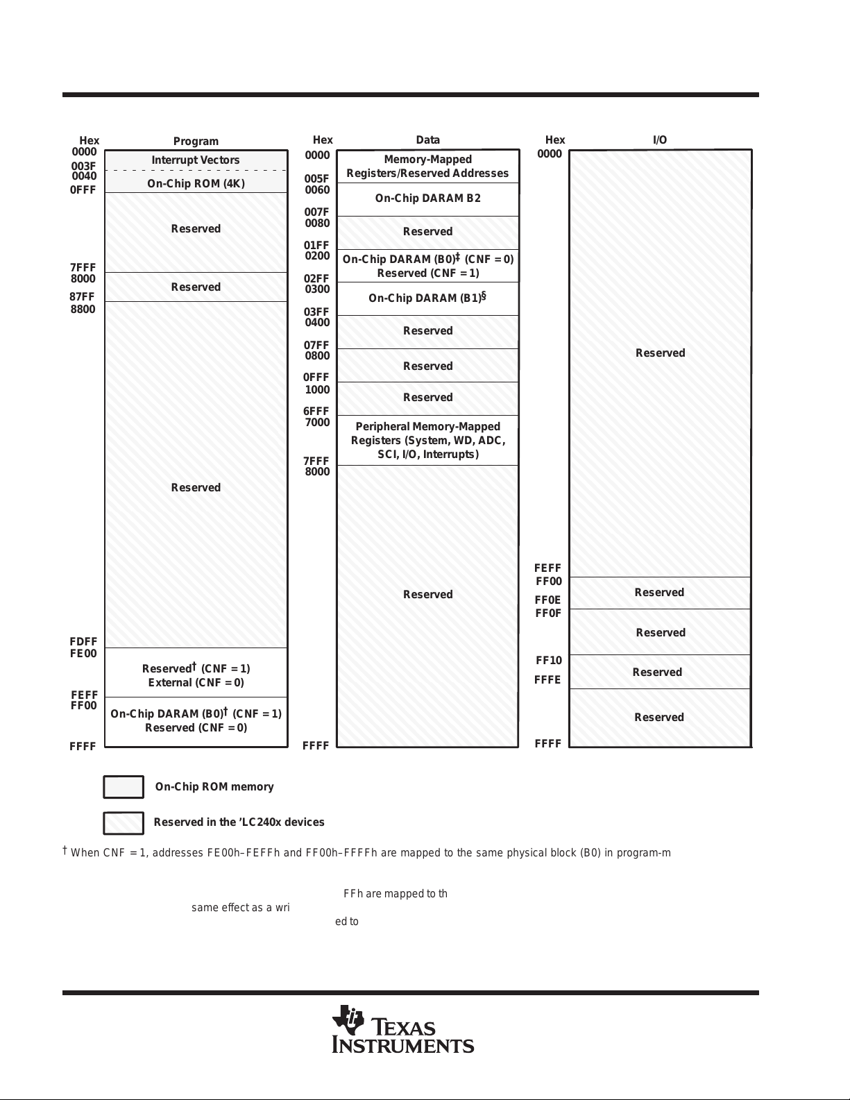
memory maps (continued) – ’LC2404
Reserved
Reserved
On-Chip ROM
16K
Reserved
Program
Interrupt Vectors
Hex Data
Memory-Mapped
Registers/Reserved Addresses
On-Chip DARAM B2
Reserved
On-Chip DARAM (B0)
‡
(CNF = 0)
Reserved (CNF = 1)
On-Chip DARAM (B1)
§
Reserved
SARAM (1K) (DON = 1)
Internal
Reserved (DON = 0)
Reserved
Peripheral Memory-Mapped
Registers (System, WD, ADC,
SCI, SPI, I/O, Interrupts)
Hex I/O
Reserved
Reserved
†
(CNF = 1)
External (CNF = 0)
On-Chip DARAM (B0)
†
(CNF = 1)
Reserved (CNF = 0)
Reserved
Reserved
SARAM (See Table 1 for details.)
On-Chip ROM memory
Reserved in the ’LC240x devices
Reserved
0000
003F
0040
Hex
7FFF
8000
FFFF
FEFF
FF00
FDFF
FE00
83FF
8400
0000
005F
0060
007F
0080
01FF
0200
02FF
0300
03FF
0400
07FF
0800
6FFF
7000
7FFF
8000
FFFF
0BFF
0C00
0000
FEFF
FF00
FF0E
FF0F
FFFF
FFFE
FF10
SARAM (1K) (PON = 1)
Internal
Reserved (PON = 0)
Reserved
3FFF
4000
†
When CNF = 1, addresses FE00h–FEFFh and FF00h–FFFFh are mapped to the same physical block (B0) in program-memory space. For
example, a write to FE00h has the same effect as a write to FF00h. For simplicity, addresses FE00h–FEFFh are referred to as reserved when
CNF = 1.
‡
When CNF = 0, addresses 0100h–01FFh and 0200h–02FFh are mapped to the same physical block (B0) in data-memory space. For example,
a write to 0100h has the same effect as a write to 0200h. For simplicity , addresses 0100h–01FFh are referred to as reserved.
§
Addresses 0300h–03FFh and 0400h–04FFh are mapped to the same physical block (B1) in data-memory space. For example, a write to 0400h
has the same effect as a write to 0300h. For simplicity , addresses 0400h–04FFh are referred to as reserved.
Figure 5. TMS320LC2404 Memory Map
ADVANCE
INFORMATION
TMS320LF2407, TMS320LF2406, TMS320LF2402
TMS320LC2406, TMS320LC2404, TMS320LC2402
DSP CONTROLLERS
SPRS094C – APRIL 1999 – REVISED OCTOBER 1999
20
POST OFFICE BOX 1443 • HOUSTON, TEXAS 77251–1443
memory maps (continued) – ’LC2402
Reserved
Reserved
On-Chip ROM (4K)
Reserved
Program
Interrupt Vectors
Hex Data
Memory-Mapped
Registers/Reserved Addresses
On-Chip DARAM B2
Reserved
On-Chip DARAM (B0)
‡
(CNF = 0)
Reserved (CNF = 1)
On-Chip DARAM (B1)
§
Reserved
Reserved
Peripheral Memory-Mapped
Registers (System, WD, ADC,
SCI, I/O, Interrupts)
Hex I/O
Reserved
Reserved
†
(CNF = 1)
External (CNF = 0)
On-Chip DARAM (B0)
†
(CNF = 1)
Reserved (CNF = 0)
Reserved
Reserved
On-Chip ROM memory
Reserved in the ’LC240x devices
Reserved
0000
003F
Hex
8000
FFFF
FEFF
FF00
FDFF
FE00
87FF
8800
0000
005F
0060
007F
0080
01FF
0200
02FF
0300
03FF
0400
07FF
0800
6FFF
7000
7FFF
8000
FFFF
0FFF
1000
0000
FEFF
FF00
FF0E
FF0F
FFFF
FFFE
FF10
7FFF
Reserved
Reserved
Reserved
0FFF
0040
†
When CNF = 1, addresses FE00h–FEFFh and FF00h–FFFFh are mapped to the same physical block (B0) in program-memory space. For
example, a write to FE00h has the same effect as a write to FF00h. For simplicity, addresses FE00h–FEFFh are referred to as reserved when
CNF = 1.
‡
When CNF = 0, addresses 0100h–01FFh and 0200h–02FFh are mapped to the same physical block (B0) in data-memory space. For example,
a write to 0100h has the same effect as a write to 0200h. For simplicity , addresses 0100h–01FFh are referred to as reserved.
§
Addresses 0300h–03FFh and 0400h–04FFh are mapped to the same physical block (B1) in data-memory space. For example, a write to 0400h
has the same effect as a write to 0300h. For simplicity , addresses 0400h–04FFh are referred to as reserved.
Figure 6. TMS320LC2402 Memory Map
ADVANCE
INFORMATION
TMS320LF2407, TMS320LF2406, TMS320LF2402
TMS320LC2406, TMS320LC2404, TMS320LC2402
DSP CONTROLLERS
SPRS094C – APRIL 1999 – REVISED OCTOBER 1999
21
POST OFFICE BOX 1443 • HOUSTON, TEXAS 77251–1443
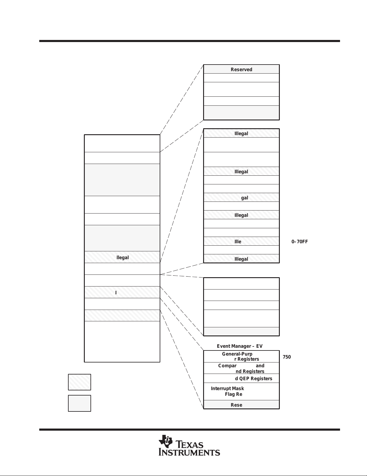
peripheral memory map of the ’LF240x/’LC240x
Illegal
Illegal
Illegal
Illegal
Illegal
Illegal
Illegal
Illegal
Reserved
Reserved
70C0–70FF
General-Purpose
Timer Registers
Flag Registers
Event Manager – EVB
Deadband Registers
Compare, PWM, and
Interrupt Mask, Vector, and
Capture and QEP Registers
7500–7508
7511–7519
7520–7529
752C–7531
7532–753F
7432–743F
742C–7431
7420–7429
7411–7419
7400–7408
Reserved
Flag Registers
Interrupt Mask, Vector and
Capture and QEP Registers
Deadband Registers
Compare, PWM, and
Timer Registers
General-Purpose
Event Manager – EVA
7230–73FF
7100–722F
70A0–70BF
7090–709F
7080–708F
7070–707F
7060–706F
7050–705F
7040–704F
7030–703F
7020–702F
7010–701F
7000–700F
CAN Control Registers
ADC Control Registers
Digital I/O Control Registers
External-Interrupt Registers
SCI
SPI
Watchdog Timer Registers
Control Registers
System Configuration and
Hex
Hex
005F
0007
0006
0005
0004
0003
0000
and Reserved
Emulation Registers
Interrupt Flag Register
Register (Reserved)
Global-Memory Allocation
Interrupt-Mask Register
FFFF
8000
7FFF
7540
753F
7500
74FF
7440
743F
7400
73FF
7000
6FFF
0800
07FF
0400
03FF
0300
02FF
0200
01FF
0080
007F
0060
005F
0000
External
Illegal
Peripheral Frame 3 (PF3)
Peripheral Frame 2 (PF2)
Peripheral Frame 1 (PF1)
Reserved
On-Chip DARAM B1
On-Chip DARAM B0
Reserved
On-Chip DARAM B2
and Reserved
Memory-Mapped Registers
“Illegal” indicates that access to
these addresses causes a
nonmaskable interrupt (NMI).
Reserved
Illegal
“Reserved” indicates addresses that
are reserved for test and future expansion.
ADVANCE
INFORMATION

TMS320LF2407, TMS320LF2406, TMS320LF2402
TMS320LC2406, TMS320LC2404, TMS320LC2402
DSP CONTROLLERS
SPRS094C – APRIL 1999 – REVISED OCTOBER 1999
22
POST OFFICE BOX 1443 • HOUSTON, TEXAS 77251–1443
device reset and interrupts
The TMS320x240x software-programmable interrupt structure supports flexible on-chip and external interrupt
configurations to meet real-time interrupt-driven application requirements. The ’LF240x recognizes three types
of interrupt sources.
D Reset (hardware- or software-initiated) is unarbitrated by the CPU and takes immediate priority over any
other executing functions. All maskable interrupts are disabled until the reset service routine enables them.
The ’LF240x devices have two sources of reset: an external reset pin and a watchdog timer timeout (reset).
D Hardware-generated interrupts are requested by external pins or by on-chip peripherals. There are two
types:
–
External interrupts
are generated by one of four external pins corresponding to the interrupts XINT1,
XINT2, PDPINT A, and PDPINTB. These four can be masked both by dedicated enable bits and by t he
CPU’s interrupt mask register (IMR), which can mask each maskable interrupt line at the DSP core.
–
Peripheral interrupts
are initiated internally by these on-chip peripheral modules: event manager A,
event manager B, SPI, SCI, WD, CAN, and ADC. They can be masked both by enable bits for each
event in each peripheral and by the CPU’s IMR, which can mask each maskable interrupt line at the DSP
core.
D Software-generated interrupts for the ’LF240x devices include:
–
The INTR instruction.
This instruction allows initialization of any ’LF240x interrupt with software. Its
operand indicates the interrupt vector location to which the CPU branches. This instruction globally
disables maskable interrupts (sets the INTM bit to 1).
–
The NMI instruction.
This instruction forces a branch to interrupt vector location 24h. This instruction
globally disables maskable interrupts. ’240x devices do not have the NMI hardware signal, only
software activation is provided.
–
The TRAP instruction.
This instruction forces the CPU to branch to interrupt vector location 22h. The
TRAP instruction does
not
disable maskable interrupts (INTM is not set to 1); therefore, when the CPU
branches to the interrupt service routine, that routine can be interrupted by the maskable hardware
interrupts.
–
An emulator trap.
This interrupt can be generated with either an INTR instruction or a TRAP instruction.
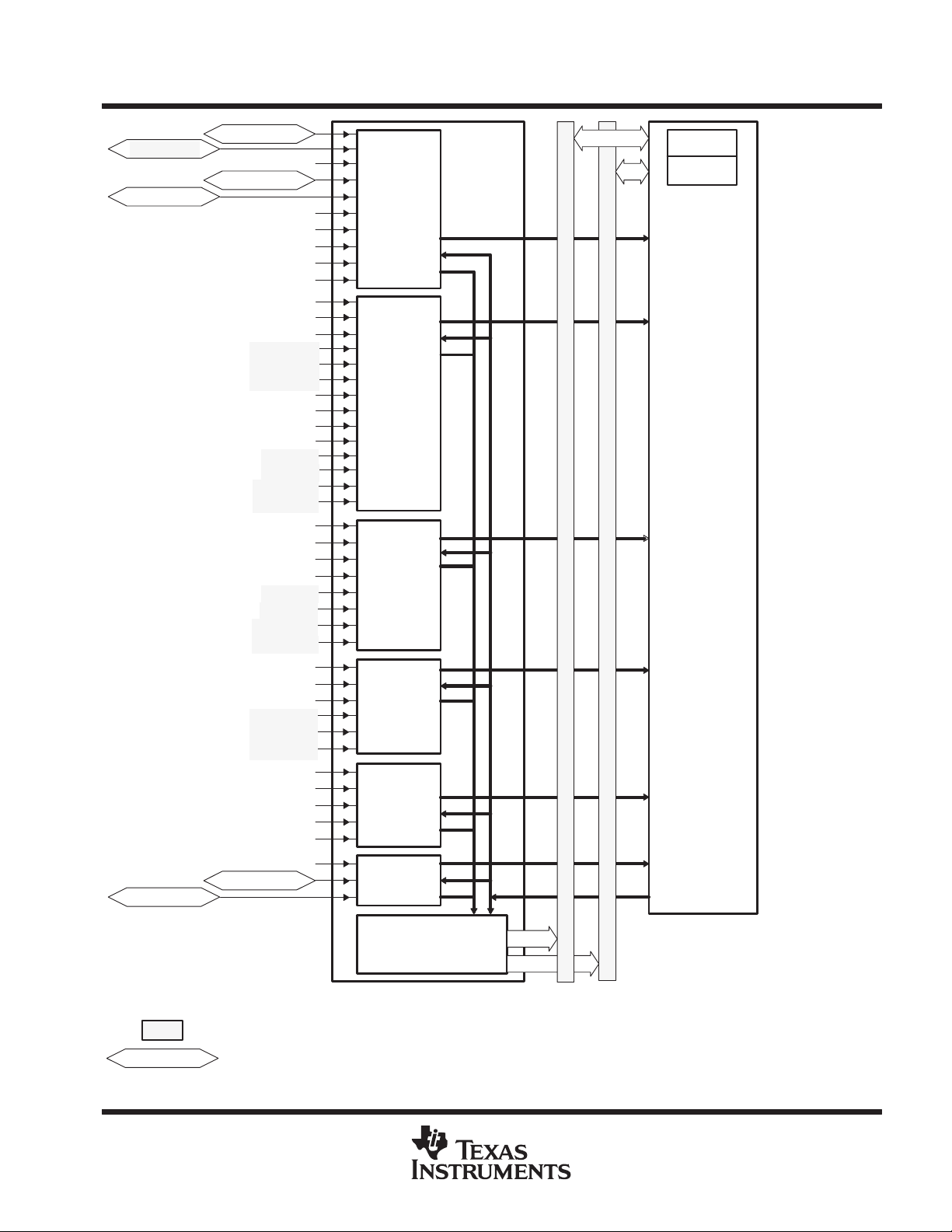
Six core interrupts (INT1–INT6) are expanded using a peripheral interrupt expansion (PIE) module identical to
the ’F24x devices. The PIE manages all the peripheral interrupts from the ’240x peripherals and are grouped to
share the six-core level interrupts. Figure 7 shows the PIE block diagram for hardware-generated interrupts.
The PIE diagram (Figure 7) and the interrupt table (Table 3) explain the grouping and interrupt vector maps.
’LF240x devices have interrupts identical to the ’F24x devices and should be completely code-compatible.
’240x devices also have peripheral interrupts identical to the ’F24x – plus additional interrupts for new
peripherals such as event manager B. Though the new interrupts share the ’24x interrupt grouping, they all have
a unique vector to differentiate among the interrupts. See Table 3 for details.
ADVANCE
INFORMATION
TMS320LF2407, TMS320LF2406, TMS320LF2402
TMS320LC2406, TMS320LC2404, TMS320LC2402
DSP CONTROLLERS
SPRS094C – APRIL 1999 – REVISED OCTOBER 1999
23
POST OFFICE BOX 1443 • HOUSTON, TEXAS 77251–1443
CPU
IACK
Addr
Bus
Data
Bus
PIVR & Logic
PIRQR#
PIACK#
IRQ GEN
Level 6
IRQ GEN
Level 5
IRQ GEN
Level 4
IRQ GEN
Level 3
IRQ GEN
Level 2
IRQ GEN
Level 1
ADCINT
CANERINT
CANMBINT
TXINT
RXINT
SPIINT
CAP3INT
CAP2INT
CAP1INT
T2OFINT
T2UFINT
T2CINT
T2PINT
T1OFINT
T1UFINT
T1CINT
T1PINT
CMP3INT
CMP2INT
CMP1INT
CANERINT
CANMBINT
TXINT
RXINT
SPIINT
ADCINT
PDPINTB
INT1
INT2
INT3
INT4
INT6
INT5
IMR
IFR
PIE
CAP6INT
CAP5INT
CAP4INT
T4OFINT
T4UFINT
T4CINT
T4PINT
CMP6INT
CMP5INT
CMP4INT
T3OFINT
T3UFINT
T3PINT
T3CINT
PDPINTA
Indicates change with respect to the TMS320F243/F241/C242 data sheets.
XINT1
XINT2
XINT1
XINT2
Interrupts from external interrupt pins. The remaining interrupts are internal to the peripherals.
Figure 7. Peripheral Interrupt Expansion (PIE) Module Block Diagram for Hardware-Generated Interrupts
ADVANCE
INFORMATION
TMS320LF2407, TMS320LF2406, TMS320LF2402
TMS320LC2406, TMS320LC2404, TMS320LC2402
DSP CONTROLLERS
SPRS094C – APRIL 1999 – REVISED OCTOBER 1999
24
POST OFFICE BOX 1443 • HOUSTON, TEXAS 77251–1443
interrupt request structure
Table 3. ’LF240x/’LC240x Interrupt Source Priority and Vectors
INTERRUPT
NAME
OVERALL
PRIORITY
CPU
INTERRUPT
AND
VECTOR
ADDRESS
BIT
POSITION IN
PIRQRx AND
PIACKRx
PERIPHERAL
INTERRUPT
VECTOR
(PIV)
MASK-
ABLE?
SOURCE
PERIPHERAL
MODULE
DESCRIPTION
Reset 1
RSN
0000h
N/A N
RS pin,
Watchdog
Reset from pin, watchdog
timeout
Reserved 2
–
0026h
N/A N CPU Emulator trap
NMI 3
NMI
0024h
N/A N
Nonmaskable
Interrupt
Nonmaskable interrupt,
software interrupt only
PDPINTA 4 0.0 0020h Y EVA
Power device protection
PDPINTB 5 2.0 0019h Y EVB
Power
device
rotection
interrupt pins
ADCINT 6
0.1 0004h Y ADC
ADC interrupt in
high-priority mode
XINT1 7 0.2 0001h Y
External
Interrupt Logic
External interrupt pins in high
priority
XINT2 8
0.3 0011h Y
External
Interrupt Logic
External interrupt pins in high
priority
SPIINT 9
INT1
0.4 0005h Y SPI SPI interrupt pins in high priority
RXINT 10
0002h
0.5 0006h Y SCI
SCI receiver interrupt in
high-priority mode
TXINT 11 0.6 0007h Y SCI
SCI transmitter interrupt in
high-priority mode
CANMBINT 12 0.7 0040 Y CAN
CAN mailbox in high-priority
mode
CANERINT 13 0.8 0041 Y CAN
CAN error interrupt in
high-priority mode
CMP1INT 14 0.9 0021h Y EVA Compare 1 interrupt
CMP2INT 15 0.10 0022h Y EVA Compare 2 interrupt
CMP3INT 16 0.11 0023h Y EVA Compare 3 interrupt
T1PINT 17
0.12 0027h Y EVA Timer 1 period interrupt
T1CINT 18
INT2
0.13 0028h Y EVA Timer 1 compare interrupt
T1UFINT 19
0004h
0.14 0029h Y EVA Timer 1 underflow interrupt
T1OFINT 20 0.15 002Ah Y EVA Timer 1 overflow interrupt
CMP4INT 21 2.1 0024h Y EVB Compare 4 interrupt
CMP5INT 22 2.2 0025h Y EVB Compare 4 interrupt
CMP6INT 23 2.3 0026h Y EVB Compare 4 interrupt
T3PINT 24 2.4 002Fh Y EVB Timer 3 period interrupt
T3CINT 25 2.5 0030h Y EVB Timer 3 compare interrupt
T3UFINT 26 2.6 0031h Y EVB Timer 3 underflow interrupt
T3OFINT 27 2.7 0032h Y EVB Timer 3 overflow interrupt
†
Refer to the
TMS320C240 DSP Controllers CPU, System, and Instruction Set Reference Guide
(literature number SPRU160) and the
TMS320F243/’F241/’C242 DSP Controllers System and Peripherals User’s Guide
(literature number SPRU276) for more information.
New peripheral interrupts and vectors with respect to the ’F243/’F241 devices.
ADVANCE
INFORMATION
TMS320LF2407, TMS320LF2406, TMS320LF2402
TMS320LC2406, TMS320LC2404, TMS320LC2402
DSP CONTROLLERS
SPRS094C – APRIL 1999 – REVISED OCTOBER 1999
25
POST OFFICE BOX 1443 • HOUSTON, TEXAS 77251–1443
interrupt request structure (continued)
Table 3.’LF240x/’LC240x Interrupt Source Priority and Vectors (Continued)
INTERRUPT
NAME
OVERALL
PRIORITY
CPU
INTERRUPT
AND
VECTOR
ADDRESS
BIT
POSITION IN
PIRQRx AND
PIACKRx
PERIPHERAL
INTERRUPT
VECTOR
(PIV)
MASK-
ABLE?
SOURCE
PERIPHERAL
MODULE
DESCRIPTION
T2PINT 28 1.0 002Bh Y EVA Timer 2 period interrupt
T2CINT 29 1.1 002Ch Y EVA Timer 2 compare interrupt
T2UFINT 30 1.2 002Dh Y EVA Timer 2 underflow interrupt
T2OFINT 31
INT3
1.3 002Eh Y EVA Timer 2 overflow interrupt
T4PINT 32
INT3
0006h
2.8 0039h Y EVB Timer 4 period interrupt
T4CINT 33 2.9 003Ah Y EVB Timer 4 compare interrupt
T4UFINT 34 2.10 003Bh Y EVB Timer 4 underflow interrupt
T4OFINT 35 2.11 003Ch Y EVB Timer 4 overflow interrupt
CAP1INT 36 1.4 0033h Y EVA Capture 1 interrupt
CAP2INT 37 1.5 0034h Y EVA Capture 2 interrupt
CAP3INT 38
INT4
1.6 0035h Y EVA Capture 3 interrupt
CAP4INT 39
INT4
0008h
2.12 0036h Y EVB Capture 4 interrupt
CAP5INT 40 2.13 0037h Y EVB Capture 5 interrupt
CAP6INT 41 2.14 0038h Y EVB Capture 6 interrupt
SPIINT 42 1.7 0005h Y SPI SPI interrupt (low priority)
RXINT 43 1.8 0006h Y SCI
SCI receiver interrupt
(low-priority mode)
TXINT 44
INT5
1.9 0007h Y SCI
SCI transmitter interrupt
(low-priority mode)
CANMBINT 45
000Ah
1.10 0040h Y CAN
CAN mailbox interrupt
(low-priority mode)
CANERINT 46 1.11 0041h Y CAN
CAN error interrupt
(low-priority mode)
ADCINT 47 1.12 0004h Y ADC
ADC interrupt
(low priority)
XINT1 48
INT6
000Ch
1.13 0001h Y
External
Interrupt Logic
External interrupt pins
(low-priority mode)
XINT2 49
000Ch
1.14 0011h Y
External
Interrupt Logic
External interrupt pins
(low-priority mode)
Reserved 000Eh N/A Y CPU Analysis interrupt
TRAP N/A 0022h N/A N/A CPU TRAP instruction
Phantom
Interrupt
Vector
N/A N/A 0000h N/A CPU Phantom interrupt vector
INT8–INT16 N/A 0010h–0020h N/A N/A CPU
INT20–INT31 N/A 00028h–0603Fh N/A N/A CPU
Software interrupt vectors
†
†
Refer to the
TMS320C240 DSP Controllers CPU, System, and Instruction Set Reference Guide
(literature number SPRU160) and the
TMS320F243/’F241/’C242 DSP Controllers System and Peripherals User’s Guide
(literature number SPRU276) for more information.
New peripheral interrupts and vectors with respect to the ’F243/’F241 devices.
ADVANCE
INFORMATION

TMS320LF2407, TMS320LF2406, TMS320LF2402
TMS320LC2406, TMS320LC2404, TMS320LC2402
DSP CONTROLLERS
SPRS094C – APRIL 1999 – REVISED OCTOBER 1999
26
POST OFFICE BOX 1443 • HOUSTON, TEXAS 77251–1443
DSP CPU Core
The TMS320x240x devices use an advanced Harvard-type architecture that maximizes processing power by
maintaining two separate memory bus structures — program and data — for full-speed execution. This multiple
bus structure allows data and instructions to be read simultaneously. Instructions support data transfers
between program memory and data memory . This architecture permits coefficients that are stored in program
memory to be read in RAM, thereby eliminating the need for a separate coefficient ROM. This, coupled with a
four-deep pipeline, allows the ’LF240x/’LC240x devices to execute most instructions in a single cycle. See the
architectural block diagram of the ’24x DSP Core for more information.
TMS320x240x instruction set
The ’x240x microprocessor implements a comprehensive instruction set that supports both numeric-intensive
signal-processing operations and general-purpose applications, such as multiprocessing and high-speed
control. Source code for the ’C1x and ’C2x DSPs is upwardly compatible with the ’x243/’x241 and ’240x devices.
For maximum throughput, the next instruction is prefetched while the current one is being executed. Because
the same data lines are used to communicate to external data, program, or I/O space, the number of cycles an
instruction requires to execute varies, depending upon whether the next data operand fetch is from internal or
external memory . Highest throughput is achieved by maintaining data memory on chip and using either internal
or fast external program memory.
addressing modes
The TMS320x240x instruction set provides four basic memory-addressing modes: direct, indirect, immediate,
and register.
In direct addressing, the instruction word contains the lower seven bits of the data memory address. This field
is concatenated with the nine bits of the data memory page pointer (DP) to form the 16-bit data memory address.
Therefore, in the direct-addressing mode, data memory is paged effectively with a total of 512 pages, with each
page containing 128 words.
Indirect addressing accesses data memory through the auxiliary registers. In this addressing mode, the address
of the instruction operand is contained in the currently selected auxiliary register. Eight auxiliary registers
(AR0–AR7) provide flexible and powerful indirect addressing. T o select a specific auxiliary register , the auxiliary
register pointer (ARP) is loaded with a value from 0 to 7 for AR0 through AR7, respectively.
scan-based emulation
TMS320x2xx devices incorporate scan-based emulation logic for code-development and hardware-
development support. Scan-based emulation allows the emulator to control the processor in the system without
the use of intrusive cables to the full pinout of the device. The scan-based emulator communicates with the ’x2xx
by way of the IEEE 1149.1-compatible (JTAG) interface. The ’x240x DSPs, like the TMS320F243/241,
TMS320F206, TMS320C203, and TMS320LC203, do not include boundary scan. The scan chain of these
devices is useful for emulation function only.
ADVANCE
INFORMATION
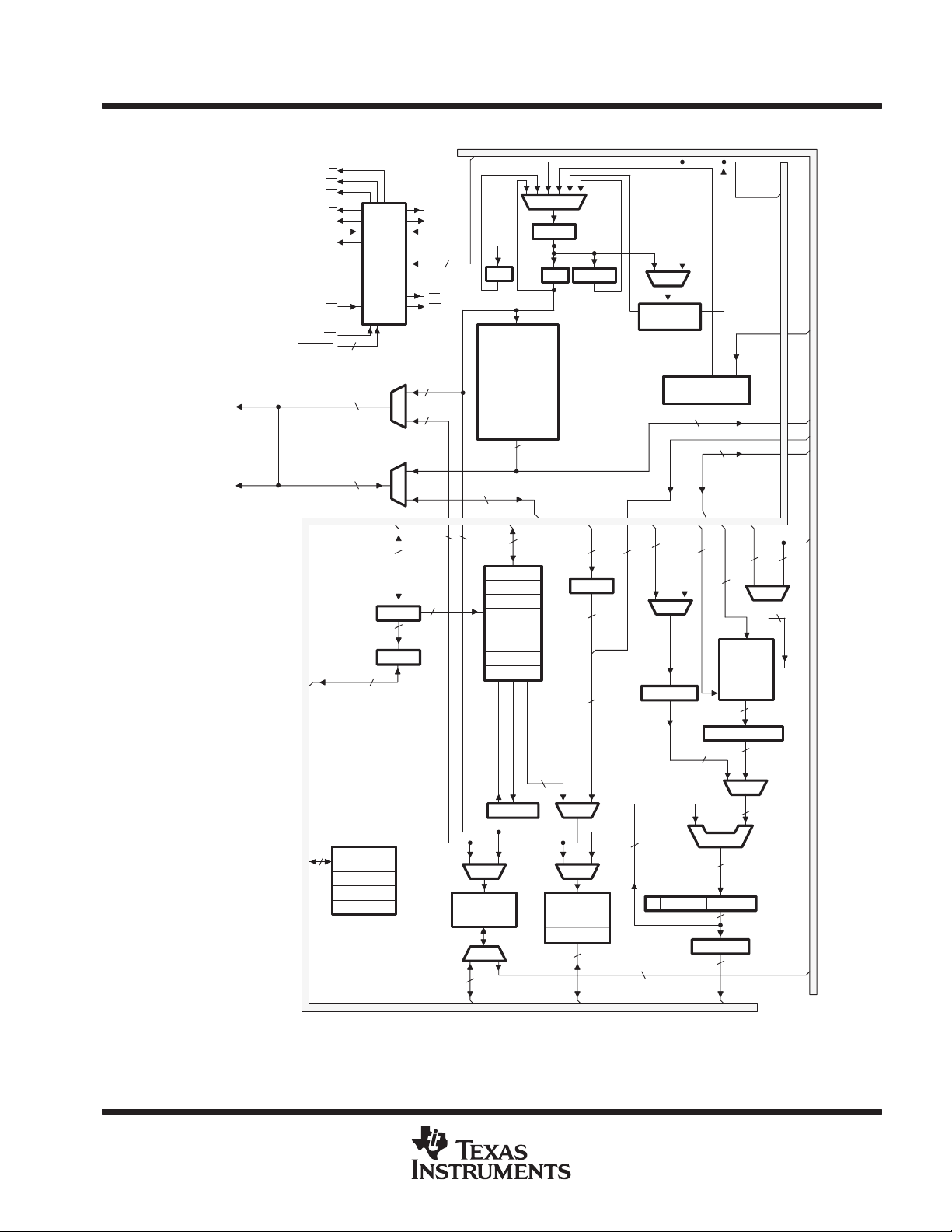
TMS320LF2407, TMS320LF2406, TMS320LF2402
TMS320LC2406, TMS320LC2404, TMS320LC2402
DSP CONTROLLERS
SPRS094C – APRIL 1999 – REVISED OCTOBER 1999
27
POST OFFICE BOX 1443 • HOUSTON, TEXAS 77251–1443
functional block diagram of the ’240x DSP CPU
32
16
Data Bus
16
OSCALE (0–7)
D15–D0
A15–A0
16
1616
32
32
ACCL(16)ACCH(16)C
32
CALU(32)
3232
MUX
ISCALE (0–16)
16
MUX
PREG(32)
Multiplier
TREG0(16)
MUX
16
16
MUX
B1 (256 × 16)
B2 (32 × 16)
DARAM
B0 (256 × 16)
DARAM
7
LSB
from
IR
MUX
DP(9)
9
9
MUX
1616
ARAU(16)
16
3
3
3
3
ARB(3)
ARP(3)
Program Bus
16
16
16
16
AR7(16)
AR6(16)
AR5(16)
AR3(16)
AR2(16)
AR1(16)
AR0(16)
Stack 8 × 16
PC
MUX
WE
RD
16
XTAL2
CLKOUT
XTAL1
2
XINT[1–2]
MP/MC
RS
XF
READY
STRB
R/W
PS
DS
IS
Control
Data Bus
Program Bus
Data Bus
AR4(16)
16
MUXMUX
Data/Prog
16
PSCALE (–6,ā0,ā1,ā4)
16
Data
32
16
16
16
16
16
FLASH EEPROM/
ROM
MUX
MUX
NPAR
PAR MST ACK
Program Control
(PCTRL)
Memory Map
Register
IMR (16)
IFR (16)
GREG (16)
16
Program Bus
NOTES: A. See T able 4 for symbol descriptions.
B. For clarity, the data and program buses are shown as single buses although they include address and data bits.
C. Refer to the TMS320F243, TMS320F241 DSP Controllers data sheet (literature number SPRS064), the TMS320C240,
TMS320F240 DSP Controllers data sheet (literature number SPRS042), and the
TMS320C240 DSP Controllers CPU, System, and
Instruction Set Reference Guide
(literature number SPRU160) for CPU instruction set information.
ADVANCE
INFORMATION
TMS320LF2407, TMS320LF2406, TMS320LF2402
TMS320LC2406, TMS320LC2404, TMS320LC2402
DSP CONTROLLERS
SPRS094C – APRIL 1999 – REVISED OCTOBER 1999
28
POST OFFICE BOX 1443 • HOUSTON, TEXAS 77251–1443
’240x legend for the internal hardware
Table 4. Legend for the ’240x DSP CPU Internal Hardware
SYMBOL NAME DESCRIPTION
ACC Accumulator
32-bit register that stores the results and provides input for subsequent CALU operations. Also includes shift
and rotate capabilities
ARAU
Auxiliary Register
Arithmetic Unit
An unsigned, 16-bit arithmetic unit used to calculate indirect addresses using the auxiliary registers as inputs
and outputs
AUX
REGS
Auxiliary Registers
0–7
These 16-bit registers are used as pointers to anywhere within the data space address range. They are
operated upon by the ARAU and are selected by the auxiliary register pointer (ARP). AR0 can also be used
as an index value for AR updates of more than one and as a compare value to AR.
C Carry
Register carry output from CALU. C is fed back into the CALU for extended arithmetic operation. The C bit
resides in status register 1 (ST1), and can be tested in conditional instructions. C is also used in accumulator
shifts and rotates.
CALU
Central Arithmetic
Logic Unit
32-bit-wide main arithmetic logic unit for the TMS320C2xx core. The CALU executes 32-bit operations in a
single machine cycle. CALU operates on data coming from ISCALE or PSCALE with data from ACC, and
provides status results to PCTRL.
DARAM Dual-Access RAM
If the on-chip RAM configuration control bit (CNF) is set to 0, the reconfigurable data dual-access RAM
(DARAM) block B0 is mapped to data space; otherwise, B0 is mapped to program space. Blocks B1 and B2
are mapped to data memory space only, at addresses 0300–03FF and 0060–007F, respectively. Blocks 0
and 1 contain 256 words, while block 2 contains 32 words.
DP
Data Memory
Page Pointer
The 9-bit DP register is concatenated with the seven least significant bits (LSBs) of an instruction word to
form a direct memory address of 16 bits. DP can be modified by the LST and LDP instructions.
GREG
Global Memory
Allocation
Register
GREG specifies the size of the global data memory space. Since the global memory space is not used in
the ’240x devices, this register is reserved.
IMR
Interrupt Mask
Register
IMR individually masks or enables the seven interrupts.
IFR
Interrupt Flag
Register
The 7-bit IFR indicates that the TMS320C2xx has latched an interrupt from one of the seven maskable
interrupts.
INT# Interrupt Traps A total of 32 interrupts by way of hardware and/or software are available.
ISCALE
Input Data-Scaling
Shifter
16- to 32-bit barrel left-shifter. ISCALE shifts incoming 16-bit data 0 to16 positions left, relative to the 32-bit
output within the fetch cycle; therefore, no cycle overhead is required for input scaling operations.
MPY Multiplier
16 × 16-bit multiplier to a 32-bit product. MPY executes multiplication in a single cycle. MPY operates either
signed or unsigned 2s-complement arithmetic multiply.
MSTACK Micro Stack
MSTACK provides temporary storage for the address of the next instruction to be fetched when program
address-generation logic is used to generate sequential addresses in data space.
MUX Multiplexer Multiplexes buses to a common input
NPAR
Next Program
Address Register
NPAR holds the program address to be driven out on the PAB in the next cycle.
OSCALE
Output
Data-Scaling
Shifter
16- to 32-bit barrel left-shifter. OSCALE shifts the 32-bit accumulator output 0 to 7 bits left for quantization
management and outputs either the 16-bit high- or low-half of the shifted 32-bit data to the data-write data
bus (DWEB).
PAR
Program Address
Register
PAR holds the address currently being driven on P AB for as many cycles as it takes to complete all memory
operations scheduled for the current bus cycle.
PC Program Counter
PC increments the value from NPAR to provide sequential addresses for instruction-fetching and sequential
data-transfer operations.
PCTRL
Program
Controller
PCTRL decodes instruction, manages the pipeline, stores status, and decodes conditional operations.
ADVANCE
INFORMATION
TMS320LF2407, TMS320LF2406, TMS320LF2402
TMS320LC2406, TMS320LC2404, TMS320LC2402
DSP CONTROLLERS
SPRS094C – APRIL 1999 – REVISED OCTOBER 1999
29
POST OFFICE BOX 1443 • HOUSTON, TEXAS 77251–1443
’240x legend for the internal hardware (continued)
Table 4. Legend for the ’240x DSP CPU Internal Hardware (Continued)
SYMBOL NAME DESCRIPTION
PREG Product Register 32-bit register holds results of 16 × 16 multiply
PSCALE
Product-Scaling
Shifter
0-, 1-, or 4-bit left shift, or 6-bit right shift of multiplier product. The left-shift options are used to manage the
additional sign bits resulting from the 2s-complement multiply. The right-shift option is used to scale down
the number to manage overflow of product accumulation in the CALU. PSCALE resides in the path from the
32-bit product shifter and from either the CALU or the data-write data bus (DWEB), and requires no cycle
overhead.
STACK Stack
STACK is a block of memory used for storing return addresses for subroutines and interrupt-service
routines, or for storing data. The ’C2xx stack is 16-bit wide and eight-level deep.
TREG
Temporary
Register
16-bit register holds one of the operands for the multiply operations. TREG holds the dynamic shift count
for the LACT, ADDT, and SUBT instructions. TREG holds the dynamic bit position for the BITT instruction.
status and control registers
Two status registers, ST0 and ST1, contain the status of various conditions and modes. These registers can
be stored into data memory and loaded from data memory , thus allowing the status of the machine to be saved
and restored for subroutines.
The load status register (LST) instruction is used to write to ST0 and ST1. The store status register (SST)
instruction is used to read from ST0 and ST1 — except for the INTM bit, which is not affected by the LST
instruction. The individual bits of these registers can be set or cleared when using the SETC and CLRC
instructions. Figure 8 shows the organization of status registers ST0 and ST1, indicating all status bits contained
in each. Several bits in the status registers are reserved and are read as logic 1s. Table 5 lists status register
field definitions.
15 13 12 11 10 9 8 0
ST0
ARP OV OVM 1 INTM DP
15 13 12 11 10 9 8 7 6 5 4 3 2 1 0
ST1
ARB CNF TC SXM C 1 1 1 1 XF 1 1 PM
Figure 8. Organization of Status Registers ST0 and ST1
Table 5. Status Register Field Definitions
FIELD FUNCTION
ARB
Auxiliary register pointer buffer . When the ARP is loaded into ST0, the old ARP value is copied to the ARB except during an LST
instruction. When the ARB is loaded by way of an LST #1 instruction, the same value is also copied to the ARP.
ARP
Auxiliary register (AR) pointer. ARP selects the AR to be used in indirect addressing. When the ARP is loaded, the old ARP value
is copied to the ARB register. ARP can be modified by memory-reference instructions when using indirect addressing, and by the
LARP, MAR, and LST instructions. The ARP is also loaded with the same value as ARB when an LST #1 instruction is executed.
C
Carry bit. C is set to 1 if the result of an addition generates a carry, or reset to 0 if the result of a subtraction generates a borrow.
Otherwise, C is reset after an addition or set after a subtraction, except if the instruction is ADD or SUB with a 16-bit shift. In these
cases, ADD can only set and SUB can only reset the carry bit, but cannot affect it otherwise. The single-bit shift and rotate
instructions also affect C, as well as the SETC, CLRC, and LST #1 instructions. Branch instructions have been provided to branch
on the status of C. C is set to 1 on a reset.
CNF
On-chip RAM configuration control bit. If CNF is set to 0, the reconfigurable data dual-access RAM blocks are mapped to data
space; otherwise, they are mapped to program space. The CNF can be modified by the SETC CNF, CLRC CNF, and LST #1
instructions. RS
sets the CNF to 0.
ADVANCE
INFORMATION
TMS320LF2407, TMS320LF2406, TMS320LF2402
TMS320LC2406, TMS320LC2404, TMS320LC2402
DSP CONTROLLERS
SPRS094C – APRIL 1999 – REVISED OCTOBER 1999
30
POST OFFICE BOX 1443 • HOUSTON, TEXAS 77251–1443
status and control registers (continued)
Table 5. Status Register Field Definitions (Continued)
FIELD FUNCTION
DP
Data memory page pointer. The 9-bit DP register is concatenated with the seven LSBs of an instruction word to form a direct
memory address of 16 bits. DP can be modified by the LST and LDP instructions.
INTM
Interrupt mode bit. When INTM is set to 0, all unmasked interrupts are enabled. When set to 1, all maskable interrupts are disabled.
INTM is set and reset by the SETC INTM and CLRC INTM instructions. RS
also sets INTM. INTM has no effect on the unmaskable
RS
and NMI interrupts. Note that INTM is unaffected by the LST instruction. This bit is set to 1 by reset. It is also set to 1 when
a maskable interrupt trap is taken.
OV
Overflow flag bit. As a latched overflow signal, OV is set to 1 when overflow occurs in the arithmetic logic unit (ALU). Once an
overflow occurs, the OV remains set until a reset, BCND/D on OV/NOV, or LST instruction clears OV .
OVM
Overflow mode bit. When OVM is set to 0, overflowed results overflow normally in the accumulator. When set to 1, the accumulator
is set to either its most positive or negative value upon encountering an overflow. The SETC and CLRC instructions set and reset
this bit, respectively. LST can also be used to modify the OVM.
PM
Product shift mode. If these two bits are 00, the multiplier’s 32-bit product is loaded into the ALU with no shift. If PM = 01, the PREG
output is left-shifted one place and loaded into the ALU, with the LSB zero-filled. If PM = 10, the PREG output is left-shifted by four
bits and loaded into the ALU, with the LSBs zero-filled. PM = 11 produces a right shift of six bits, sign-extended. Note that the PREG
contents remain unchanged. The shift takes place when transferring the contents of the PREG to the ALU. PM is loaded by the
SPM and LST #1 instructions. PM is cleared by RS
.
SXM
Sign-extension mode bit. SXM = 1 produces sign extension on data as it is passed into the accumulator through the scaling shifter.
SXM = 0 suppresses sign extension. SXM does not affect the definitions of certain instructions; for example, the ADDS instruction
suppresses sign extension regardless of SXM. SXM is set by the SETC SXM instruction and reset by the CLRC SXM instruction
and can be loaded by the LST #1 instruction. SXM is set to 1 by reset.
TC
T est/control flag bit. TC is affected by the BIT, BITT , CMPR, LST #1, and NORM instructions. TC is set to a 1 if a bit tested by BIT
or BITT is a 1, if a compare condition tested by CMPR exists between AR (ARP) and AR0, if the exclusive-OR function of the two
most significant bits (MSBs) of the accumulator is true when tested by a NORM instruction. The conditional branch, call, and return
instructions can execute based on the condition of TC.
XF
XF pin status bit. XF indicates the state of the XF pin, a general-purpose output pin. XF is set by the SETC XF instruction and reset
by the CLRC XF instruction. XF is set to 1 by reset.
central processing unit
The TMS320x240x central processing unit (CPU) contains a 16-bit scaling shifter, a 16 x 16-bit parallel
multiplier, a 32-bit central arithmetic logic unit (CALU), a 32-bit accumulator, and additional shifters at the
outputs of both the accumulator and the multiplier. This section describes the CPU components and their
functions. The functional block diagram shows the components of the CPU.
input scaling shifter
The TMS320x240x provides a scaling shifter with a 16-bit input connected to the data bus and a 32-bit output
connected to the CALU. This shifter operates as part of the path of data coming from program or data space
to the CALU and requires no cycle overhead. It is used to align the 16-bit data coming from memory to the 32-bit
CALU. This is necessary for scaling arithmetic as well as aligning masks for logical operations.
The scaling shifter produces a left shift of 0 to 16 on the input data. The LSBs of the output are filled with zeros;
the MSBs can either be filled with zeros or sign-extended, depending upon the value of the SXM bit
(sign-extension mode) of status register ST1. The shift count is specified by a constant embedded in the
instruction word or by a value in TREG. The shift count in the instruction allows for specific scaling or alignment
operations specific to that point in the code. The TREG base shift allows the scaling factor to be adaptable to
the system’s performance.
ADVANCE
INFORMATION
 Loading...