


 Loading...
Texas instruments TMS320F28062, TMS320F28068, TMS320F28067, TMS320F28069, TMS320F28064 ADVANCE INFORMATION
...TMS320F28069, TMS320F28068, TMS320F28067, TMS320F28066
TMS320F28065, TMS320F28064, TMS320F28063, TMS320F28062
www.ti.com |
SPRS698A –NOVEMBER 2010 –REVISED JANUARY 2011 |
Piccolo Microcontrollers
Check for
Samples: TMS320F28069, TMS320F28068, TMS320F28067, TMS320F28066, TMS320F28065, TMS320F28064, TMS320F28063,
TMS320F28062
1 TMS320F2806x ( Piccolo™ ) MCUs
1.1Features
•High-Efficiency 32-Bit CPU (TMS320C28x™ )
–80 MHz (12.5-ns Cycle Time)
–16 x 16 and 32 x 32 MAC Operations
–16 x 16 Dual MAC
–Harvard Bus Architecture
–Atomic Operations
–Fast Interrupt Response and Processing
–Unified Memory Programming Model
–Code-Efficient (in C/C++ and Assembly)
•Floating-Point Unit
–Native Single-Precision Floating-Point Operations
•Programmable Control Law Accelerator (CLA)
–32-Bit Floating-Point Math Accelerator
–Executes Code Independently of the Main CPU
•Viterbi, Complex Math, CRC Unit (VCU)
–Extends C28x™ Instruction Set to Support Complex Multiply, Viterbi Operations, and Cyclic Redundency Check (CRC)
•Embedded Memory
–Up to 256KB Flash
–Up to 100KB RAM
–2KB OTP ROM
•6-Channel DMA
•Low Device and System Cost
–Single 3.3-V Supply
–No Power Sequencing Requirement
–Integrated Power-on Reset and Brown-out Reset
–Low-Power Operating Modes
–No Analog Support Pin
•Clocking
–Two Internal Zero-pin Oscillators
–On-Chip Crystal Oscillator/External Clock Input
–Dynamic PLL Ratio Changes Supported
–Watchdog Timer Module
–Missing Clock Detection Circuitry
•Peripheral Interrupt Expansion (PIE) Block That Supports All Peripheral Interrupts
•Three 32-Bit CPU Timers
•Advanced Control Peripherals
•Up to 8 Enhanced Pulse Width Modulator (ePWM) Modules
–16 PWM Channels Total (8 HRPWM-Capable)
–Independent 16-Bit Timer in Each Module
•3 Input Capture (eCAP) Modules
•4 High-Resolution Input Capture (HRCAP) Modules
•2 Quadrature Encoder (eQEP) Modules
•12-Bit ADC, Dual Sample-and-Hold
–Up to 3 MSPS
–Up to 16 Channels
•On-Chip Temperature Sensor
•128-Bit Security Key/Lock
–Protects Secure Memory Blocks
–Prevents Firmware Reverse Engineering
•Serial Port Peripherals
–Up to Two Serial Communications Interface (SCI) [UART] Modules
–Two Serial Peripheral Interface (SPI) Modules
–One Inter-Integrated-Circuit (I2C) Bus
–One Multi-Channel Buffered Serial Port (McBSP) Bus
–One Enhanced Controller Area Network (eCAN)
•Up to 54 Individually Programmable, Multiplexed GPIO Pins With Input Filtering
•Advanced Emulation Features
–Analysis and Breakpoint Functions
–Real-Time Debug via Hardware
•2806x Packages
–80-Pin PFP and 100-Pin PZP PowerPAD™ Low-Profile Quad Flatpacks (LQFPs)
–80-Pin PN and 100-Pin PZ LQFPs
Please be aware that an important notice concerning availability, standard warranty, and use in critical applications of Texas
Instruments semiconductor products and disclaimers thereto appears at the end of this data sheet.
Piccolo, PowerPAD, C28x, TMS320C2000, C2000, Code Composer Studio, XDS510, XDS560, TMS320C28x, TMS320C54x, TMS320C55x are trademarks of Texas Instruments.
All other trademarks are the property of their respective owners.
ADVANCE INFORMATION concerns new products in the sampling |
Copyright © 2010–2011, Texas Instruments Incorporated |
or preproduction phase of development. Characteristic data and other |
|
specifications are subject to change without notice. |
|
ADVANCEINFORMATION

TMS320F28069, TMS320F28068, TMS320F28067, TMS320F28066
TMS320F28065, TMS320F28064, TMS320F28063, TMS320F28062
SPRS698A –NOVEMBER 2010 –REVISED JANUARY 2011 |
www.ti.com |
1.2Description
The F2806x Piccolo™ family of microcontrollers provides the power of the C28x™ core and Control Law Accelerator (CLA) coupled with highly integrated control peripherals in low pin-count devices. This family is code-compatible with previous C28x-based code, as well as providing a high level of analog integration.
An internal voltage regulator allows for single-rail operation. Enhancements have been made to the HRPWM module to allow for dual-edge control (frequency modulation). Analog comparators with internal 10-bit references have been added and can be routed directly to control the PWM outputs. The ADC
converts from 0 to 3.3-V fixed full scale range and supports ratio-metric VREFHI/VREFLO references. The ADC interface has been optimized for low overhead/latency.
INFORMATIONADVANCE
2 |
TMS320F2806x ( Piccolo™ ) MCUs |
Copyright © 2010–2011, Texas Instruments Incorporated |
Submit Documentation Feedback
Product Folder Link(s): TMS320F28069 TMS320F28068 TMS320F28067 TMS320F28066 TMS320F28065
TMS320F28064 TMS320F28063 TMS320F28062

TMS320F28069, TMS320F28068, TMS320F28067, TMS320F28066
TMS320F28065, TMS320F28064, TMS320F28063, TMS320F28062
www.ti.com |
SPRS698A –NOVEMBER 2010 –REVISED JANUARY 2011 |
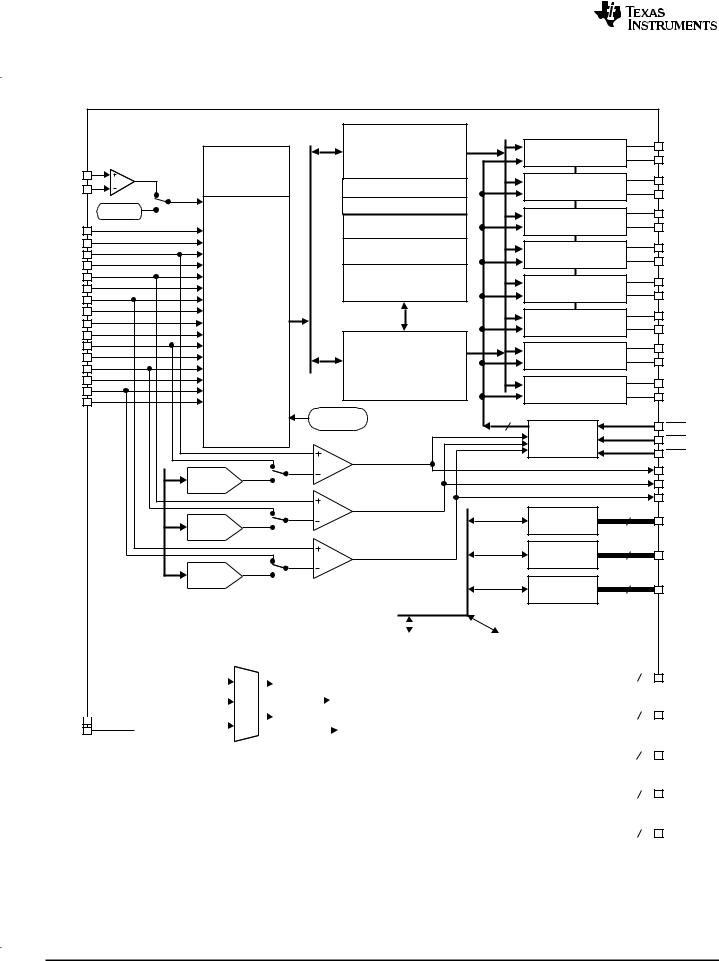
1.3Functional Block Diagram
|
|
M0 SARAM (1Kx16) |
|
|
(0-wait, Non-Secure) |
|
|
|
|
|
M1 SARAM (1Kx16) |
|
|
(0-wait, Non-Secure) |
|
|
|
|
|
|
|
|
L5 DPSARAM (8Kx16) |
|
|
(0-wait, Non-Secure) |
|
|
DMA RAM0 |
|
|
|
|
|
L6 DPSARAM (8Kx16) |
Bus |
|
(0-wait, Non-Secure) |
|
DMA RAM1 |
|
|
|
|
DMA |
|
L7 DPSARAM (8Kx16) |
|
(0-wait, Non-Secure) |
|
|
|
DMA RAM2 |
|
|
L8 DPSARAM (8Kx16) |
|
|
(0-wait, Non-Secure) |
|
|
DMA RAM3 |
|
|
|
|
DMA Bus |
|
Mux |
COMP1OUT |
|
|
GPIO |
COMP2OUT |
COMP3OUT |
|
COMP1A |
|
COMP1B |
|
COMP2A |
|
COMP2B |
|
COMP3A |
AIOMux |
COMP3B |
|
COMP  BusPeripheral
+
DAC bit-32
ADC 0-wait Result Regs
A7:0
ADC
B7:0
16-bit Peripheral Bus
L0 DPSARAM (2Kx16) |
|
|
|
|
|
|
|
|
|
|
|
OTP 1Kx16 |
|
(0-wait, Secure) |
|
|
|
|
|
|
|
|
|
|
|
Secure |
|
CLA Data RAM2 |
|
|
|
|
|
|
|
|
|
|
|
|
|
|
|
|
|
|
|
|
L1 DPSARAM (1Kx16) |
|
|
|
|
|
|
(0-wait, Secure) |
|
|
|
|
|
FLASH |
|
|
|
|
|
||
CLA Data RAM0 |
|
|
|
|
|
|
|
|
|
|
|
64K/128Kx16 |
|
|
|
|
|
|
|
|
L2 DPSARAM (1Kx16) |
|
|
Code |
|
|
8 equal sectors |
(0-wait, Secure) |
|
|
Security |
|
|
Secure |
|
|
|
|
|||
CLA Data RAM1 |
|
|
Module |
|
|
|
L3 DPSARAM (4Kx16) |
|
|
(CSM) |
|
|
|
|
|
|
|
|
|
|
(0-wait, Secure) |
|
|
|
|
|
PUMP |
|
|
|
|
|
||
CLA Program RAM |
|
|
|
|
|
|
|
|
|
|
|
|
OTP/Flash |
|
|
|
|
|
|
|
L4 SARAM (8Kx16) |
|
|
|
PSWD |
Wrapper |
|
(0-wait, Secure) |
|
|
|
|
|
|
|
|
|
|
|
|
|
|
|
|
Memory Bus |
|
|
|
Bus |
|
|
|
|
|
|
Memory |
BusCLA |
BusDMA |
Boot-ROM |
|
|
GPIO Mux |
(32Kx16) |
|
|
||||
|
|
|
|
|
|
|
|
|
|
(0-wait, |
|
|
|
|
|
|
Non-Secure) |
|
|
|
|
|
|
C28x 32-bit CPU |
TRST |
|
|
|
|
|
|
|
||
|
|
|
|
FPU |
TCK, TDI, TMS |
|
|
|
|
VCU |
|
||
|
|
|
|
|
||
|
|
|
|
|
TDO |
|
|
|
|
CLA + |
|
XCLKIN |
GPIO Mux |
|
|
|
Message |
OSC1, OSC2, |
LPM Wakeup |
|
|
|
|
RAMs |
Ext, PLLs, |
3 Ext. Interrupts |
|
|
|
|
|
LPM, WD, |
|
|
|
|
|
DMA |
CPU Timers |
X1 |
|
|
|
|
0/1/2. PIE |
X2 |
|
|
|
|
|
6-ch |
|
||
|
|
|
|
|
||
|
|
|
|
XRS |
|
|
|
|
|
|
|
|
|
CLA Bus
DMA Bus
Memory Bus
|
|
32-bit |
32-bit Peripheral Bus |
32-bit Peripheral |
Peripheral Bus |
(CLA accessible) 32-bit Peripheral |
||
(CLA accessible) |
Bus |
Bus |
SCI-A/B |
SPI-A/B |
I2C-A |
ePWM1 to ePWM8 |
McBSP-A |
|
eCAP- |
eQEP- |
HRCAP- |
eCAN-A |
|||
(4L FIFO) |
(4L FIFO) (4L FIFO) |
HRPWM (8ch) |
|
1/2/3 |
1/2 |
1/2/3/4 |
(32-mbox) |
|||||
|
|
|||||||||||
|
|
|
|
|
|
|
|
|
|
|
|
|
SCITXDx |
SCIRXDx |
SPISIMOx SPISOMIx SPICLKx SPISTEx |
SDAx |
SCLx |
TZx EPWMxA EPWMxB ESYNCI ESYNCO |
MFSRA MDRA MCLKRA MFSXA MDXA |
MCLKXA |
ECAPx |
EQEPxA EQEPxB EQEPxI EQEPxS |
HRCAPx |
CANRXx |
CANTXx |
GPIO Mux
A.Not all peripheral pins are available at the same time due to multiplexing.
Figure 1-1. Functional Block Diagram
ADVANCEINFORMATION
Copyright © 2010–2011, Texas Instruments Incorporated |
TMS320F2806x ( Piccolo™ ) MCUs |
3 |
Submit Documentation Feedback
Product Folder Link(s): TMS320F28069 TMS320F28068 TMS320F28067 TMS320F28066 TMS320F28065
TMS320F28064 TMS320F28063 TMS320F28062
INFORMATIONADVANCE
TMS320F28069, TMS320F28068, TMS320F28067, TMS320F28066
TMS320F28065, TMS320F28064, TMS320F28063, TMS320F28062
SPRS698A –NOVEMBER 2010 –REVISED JANUARY 2011 |
www.ti.com |
1.4System Device Diagram
|
|
|
C28x |
PWM1 |
|
PWM-1A |
|
|
|
Core |
|
||
|
|
ADC |
(DMA-accessible) |
|
PWM-1B |
|
|
|
(80-MHz) |
|
|||
VREFLO |
|
(DMA- |
|
|
|
|
|
|
PWM2 |
|
PWM-2A |
||
VREFHI |
accessible) |
FPU |
|
|||
|
|
(DMA-accessible) |
|
PWM-2B |
||
|
|
|
|
|
||
|
VREF |
|
VCU |
|
|
PWM-3A |
|
|
|
PWM3 |
|
||
A0 |
|
|
Flash Memory |
(DMA-accessible) |
|
PWM-3B |
|
|
|
|
|
|
|
A1 |
|
|
RAM |
PWM4 |
|
PWM-4A |
A2 |
|
|
|
|||
|
|
|
(DMA-accessible) |
|
PWM-4B |
|
A3 |
|
|
|
|
||
|
|
|
|
|
|
|
A4 |
|
|
RAM |
PWM5 |
|
PWM-5A |
A5 |
|
12-bit |
(Dual-Access) |
|
||
|
(DMA-accessible) |
|
PWM-5B |
|||
A6 |
|
|
|
|||
|
3-MSPS |
|
|
|||
|
|
|
|
|
||
A7 |
|
|
|
|
|
|
|
Dual-S/H |
|
PWM6 |
|
PWM-6A |
|
B0 |
|
|
|
|||
|
|
|
(DMA-accessible) |
|
PWM-6B |
|
B1 |
|
|
|
|
||
|
SOC- |
|
|
|
|
|
B2 |
|
CLA Core |
|
|
PWM-7A |
|
|
based |
PWM7 |
|
|||
B3 |
|
|
80-MHz Floating-Point |
(DMA-accessible) |
|
PWM-7B |
B4 |
|
|
(Accelerator) |
|
||
|
|
|
|
|
||
B5 |
|
|
(DMA-accessible) |
PWM8 |
|
PWM-8A |
B6 |
|
|
|
(DMA-accessible) |
|
PWM-8B |
B7 |
|
|
|
|
||
|
|
|
|
|
|
|
|
|
|
Temp |
6 |
|
|
|
|
|
Sensor |
|
TZ1 |
|
|
|
|
|
|
||
|
|
|
|
|
|
|
|
|
|
|
Trip Zone |
|
TZ2 |
|
|
|
CMP1-Out |
|
|
TZ3 |
|
|
|
|
|
|
|
|
10-bit |
|
|
|
|
CMP1-out |
|
|
|
|
|
CMP2-out |
|
|
DAC |
|
|
|
|
|
|
|
|
|
|
|
|
|
|
|
CMP2-Out |
|
|
CMP3-out |
|
|
|
|
|
|
|
|
10-bit |
|
|
eCAP x 3 |
3 |
eCAP |
|
|
|
|
|||
|
DAC |
|
|
|
|
|
|
|
|
CMP3-Out |
eQEP x 2 |
8 |
eQEP |
|
|
|
|
|||
|
|
|
|
|
||
|
10-bit |
|
|
|
|
|
|
DAC |
Analog |
|
HRCAP x 4 |
4 |
HRCAP |
|
|
|
|
|||
|
|
Comparators |
|
|
|
|
|
|
|
|
|
|
|
|
|
|
|
|
|
|
|
|
|
|
|
|
|
|
|
|
COMMS |
|
|
|
|
|
|
|
|
|
|
|
|
|
|
|
|
|
|
|
|
|
|
|
|
|
|
|
|
|
|
|
||
|
|
|
|
|
|
|
|
|
|
|
|
|
|
|
|
|
|
Timers 32-bit |
|
|
|
|
|
|||||
|
|
|
|
|
|
|
|
|
|
|
|
|
|
|
|
|
|
|
|
|
|
|
|
|
||||
|
|
|
|
|
|
Vreg |
|
|
|
|
|
|
|
|
|
|
|
|
|
|
|
|
|
|
|
|
|
|
|
|
|
|
|
|
|
|
|
|
|
|
|
|
|
|
|
|
|
Timer-0 |
|
|
|
UART x 2 |
|
4 |
|
|
|
|
|
|
|
|
|
|
|
|
|
|
|
|
|
|
|
|
|
|
|
|
|
|
|
|
|
|
||
|
|
|
|
|
|
Int-Osc-1 |
|
|
CLKSEL |
|
|
WD |
|
|
|
|
|
|
Timer-1 |
|
|
|
|
|
|
|
|
|
|
|
|
|
|
|
|
|
|
|
|
|
|
|
|
|
|
|
|
|
|
|
|
|
|
|
|||
X1 |
|
|
|
|
Int-Osc-2 |
|
|
PLL |
|
|
|
|
|
|
Timer-2 |
|
|
|
SPI x 2 |
8 |
|
|
||||||
|
|
|
|
|
|
|
|
|
|
|
|
|
|
|
|
|
|
|
|
|
|
|
|
|
||||
X2 |
|
|
|
|
On-chip Osc |
|
|
|
|
|
|
|
|
|
System |
|
GPIO |
|
|
|
|
2 |
|
|
||||
|
|
|
|
|
|
|
|
|
|
|
|
|
|
|
|
|
|
|
|
|||||||||
|
|
|
|
|
|
|
|
|
|
|
|
|
|
|
|
|
|
|
|
|
||||||||
|
|
|
|
|
|
|
|
|
|
|
|
|
|
|
|
|
|
|
|
|
|
|
|
|
|
|||
|
|
|
|
|
|
POR/BOR |
|
|
|
|
|
|
|
|
|
|
|
|
Control |
|
|
I2C |
|
|
|
|||
|
|
|
|
|
|
|
|
|
|
|
|
|
|
|
|
|
|
|
|
|
|
|
||||||
|
|
|
|
|
|
|
|
|
|
|
|
|
|
|
|
|
|
|
|
|
|
|
|
|
2 |
|
|
|
|
|
|
|
|
|
|
|
|
|
|
|
|
|
|
|
|
|
|
|
|
|
|
|
|
|
|
|
|
|
|
|
|
|
|
|
|
|
|
|
|
|
|
|
|
|
|
|
|
|
|
|
|
CAN |
|
|
|
|
|
|
|
|
|
|
|
|
|
|
|
|
|
|
|
|
|
|
|
|
|
|
|
|
|
|
|
||
|
|
|
|
|
|
|
|
|
|
|
|
|
|
|
|
|
|
|
|
|
|
|
|
|
6 |
|
|
|
|
|
|
|
|
|
|
|
|
|
|
|
|
|
|
|
|
|
|
|
|
|
|
|
|
|
|
|
|
|
|
|
|
|
|
|
|
|
|
|
|
|
|
|
|
|
|
|
|
|
|
|
|
|
|
|
||
|
|
|
|
|
|
|
|
|
|
|
|
|
|
|
|
|
|
|
|
|
|
|
|
McBSP |
|
|
|
|
|
|
|
|
|
|
|
|
|
|
|
|
|
|
|
|
|
|
|
|
|
|
|
|
|
||||
|
|
|
|
|
|
|
|
|
|
|
|
|
|
|
|
|
|
|
|
|
|
|
|
(DMA-accessible) |
|
|
|
|
|
|
|
|
|
|
|
|
|
|
|
|
|
|
|
|
|
|
|
|
|
|
|
|
|
|
|||
|
|
|
|
|
|
|
|
|
|
|
|
|
|
|
|
|
|
|
|
|
|
|
|
|
|
|
|
|
|
|
|
|
|
|
|
|
|
|
|
|
|
|
|
|
|
|
|
|
|
|
|
|
|
|
|
|
|
Figure 1-2. Peripheral Blocks
4 |
TMS320F2806x ( Piccolo™ ) MCUs |
Copyright © 2010–2011, Texas Instruments Incorporated |
Submit Documentation Feedback
Product Folder Link(s): TMS320F28069 TMS320F28068 TMS320F28067 TMS320F28066 TMS320F28065
TMS320F28064 TMS320F28063 TMS320F28062

TMS320F28069, TMS320F28068, TMS320F28067, TMS320F28066
TMS320F28065, TMS320F28064, TMS320F28063, TMS320F28062
www.ti.com |
SPRS698A –NOVEMBER 2010 –REVISED JANUARY 2011 |
1 |
TMS320F2806x ( Piccolo™ ) MCUs .................. |
1 |
|
|
1.1 |
Features .............................................. |
1 |
|
1.2 |
Description ........................................... |
2 |
|
1.3 |
Functional Block Diagram ............................ |
3 |
|
1.4 |
System Device Diagram ............................. |
4 |
2 |
Revision History ......................................... |
6 |
|
3 |
Device Overview ........................................ |
7 |
|
|
3.1 |
Device Characteristics ............................... |
7 |
|
3.2 |
Memory Maps ...................................... |
10 |
|
3.3 |
Pin Assignments .................................... |
20 |
|
3.4 |
Signal Descriptions ................................. |
22 |
|
3.5 |
Brief Descriptions ................................... |
31 |
|
3.6 |
Register Map ....................................... |
40 |
|
3.7 |
Device Emulation Registers ........................ |
42 |
|
3.8 |
VREG/BOR/POR ................................... |
43 |
|
3.9 |
System Control ..................................... |
45 |
|
3.10 |
Low-power Modes Block ........................... |
53 |
4 Device and Documentation Support ............... |
54 |
||
|
4.1 |
Getting Started ..................................... |
54 |
|
4.2 |
Development Support .............................. |
54 |
4.3Device and Development Support Tool
|
|
Nomenclature ....................................... |
54 |
|
4.4 |
Documentation Support ............................ |
56 |
|
4.5 |
Community Resources ............................. |
57 |
5 |
Device Operating Conditions ....................... |
58 |
|
|
5.1 |
Absolute Maximum Ratings ........................ |
58 |
|
5.2 |
Recommended Operating Conditions .............. |
58 |
|
5.3 |
Electrical Characteristics ........................... |
59 |
6 |
Peripheral and Electrical Specifications .......... |
60 |
|
|
6.1 |
Parameter Information .............................. |
60 |
6.2 |
Test Load Circuit ................................... |
60 |
6.3 |
Device Clock Table ................................. |
61 |
6.4 |
Clock Requirements and Characteristics ........... |
63 |
6.5 |
Power Sequencing ................................. |
64 |
6.6 |
Current Consumption ............................... |
67 |
6.7Emulator Connection Without Signal Buffering for
|
|
the MCU ............................................ |
69 |
6.8 |
|
Interrupts ............................................ |
70 |
6.9 |
Control Law Accelerator (CLA) Overview .......... |
75 |
|
6.10 |
Analog Block ........................................ |
78 |
|
6.11 |
Detailed Descriptions ............................... |
92 |
|
6.12 |
Serial Peripheral Interface (SPI) Module ........... |
93 |
|
6.13Serial Communications Interface (SCI) Module
..................................................... 102
6.14Multichannel Buffered Serial Port (McBSP) Module
..................................................... 105
6.15Enhanced Controller Area Network (eCAN) Module
..................................................... |
115 |
6.16 Inter-Integrated Circuit (I2C) ...................... |
119 |
6.17Enhanced Pulse Width Modulator (ePWM) Modules
|
(ePWM1/2/3/4/5/6/7/8) ............................ |
122 |
6.18 |
High-Resolution PWM (HRPWM) ................. |
129 |
6.19 |
Enhanced Capture Module (eCAP1) .............. |
130 |
6.20 |
High-Resolution Capture (HRCAP) Module ....... |
132 |
6.21Enhanced Quadrature Encoder Modules (eQEP1/2)
|
..................................................... |
133 |
6.22 |
JTAG Port ......................................... |
136 |
6.23 |
General-Purpose Input/Output (GPIO) MUX ...... |
137 |
6.24 |
Flash Timing ....................................... |
149 |
7 Mechanical Packaging and Orderable |
|
|
Information ............................................ |
151 |
|
7.1 |
Thermal Data ...................................... |
151 |
7.2 |
Packaging Information ............................ |
152 |
ADVANCEINFORMATION
Copyright © 2010–2011, Texas Instruments Incorporated |
Contents |
5 |
Submit Documentation Feedback
Product Folder Link(s): TMS320F28069 TMS320F28068 TMS320F28067 TMS320F28066 TMS320F28065
TMS320F28064 TMS320F28063 TMS320F28062

TMS320F28069, TMS320F28068, TMS320F28067, TMS320F28066
TMS320F28065, TMS320F28064, TMS320F28063, TMS320F28062
SPRS698A –NOVEMBER 2010 –REVISED JANUARY 2011 |
www.ti.com |
2 Revision History
This data sheet revision history highlights the technical changes made to the SPRS698 device-specific data sheet to make it an SPRS698A revision.
Scope: Added 80-pin PN package and 100-pin PZ package.
Added "T" temperature range (–40°C to 105°C).
|
Added new sections. |
|||
|
Information/data on the TMS320F2806x devices is now Advance Information. |
|||
|
ADVANCE INFORMATION concerns new products in the sampling or preproduction phase of |
|||
|
development. Characteristic data and other specifications are subject to change without notice. |
|||
|
|
|
|
|
|
LOCATION |
|
ADDITIONS, DELETIONS, AND MODIFICATIONS |
|
|
|
|
|
|
|
Global |
• Added 80-pin PN package |
||
|
|
|||
|
|
• Added 100-pin PZ package |
||
|
|
• Added "T" temperature range (–40°C to 105°C) |
||
|
|
|
|
|
ADVANCEINFORMATION |
Section 1 |
• Added Section 1.2, Description |
||
TMS320F2806x |
||||
• Figure 1-1, Functional Block Diagram: |
||||
(Piccolo™ ) MCUs |
||||
|
– Removed "32-bit Peripheral Bus" |
|||
|
|
|||
|
|
|
||
Section 3 |
• |
Table 3-1, Hardware Features: |
||
Device Overview |
||||
|
– 6-Channel DMA: Added "0" to TYPE column |
|||
|
|
|||
|
|
– High-resolution capture modules (HRCAP): Added "0" to TYPE column |
||
|
|
– Multi-Channel Buffered Serial Port (McBSP): Added "1" to TYPE column |
||
|
• |
– Updated "Temperature options" |
||
|
Added Section 3.8, VREG/BOR/POR |
|||
|
|
• Added Section 3.2, Memory Maps |
||
|
|
• Figure 3-8, 80-Pin PN/PFP LQFP (Top View): |
||
|
|
|
– Removed SCI-B signals and eQEP2 signals |
|
|
|
• |
Table 3-6, Terminal Functions: |
|
|
|
|
– Added "SCI-B is only available in the PZ and PZP packages" note to DESCRIPTION of PN/PFP pins# 39, |
|
|
|
|
59, 76, 70, 41, 52, 78, 1 |
|
|
|
|
– Added "eQEP2 is only available in the PZ and PZP packages" note to DESCRIPTION of PN/PFP |
|
|
|
|
pins# 77, 31, 62, 61, 33, 32 |
|
|
|
• Added Section 3.5, Brief Descriptions |
||
|
|
• Added Section 3.6, Register Map |
||
|
|
• Added Section 3.7, Device Emulation Registers |
||
|
|
• Added Section 3.9, System Control |
||
|
|
• Added Section 3.10, Low-power Modes Block |
||
|
|
|
|
|
|
Section 4 |
• Added Section 4.1, Getting Started |
||
|
Device and |
|||
|
• |
Section 4.3, Device and Development Support Tool Nomenclature: |
||
|
Documentation Support |
|||
|
|
|
– Updated PACKAGE TYPE in Figure 4-1, Device Nomenclature |
|
|
|
• Added Section 4.4, Documentation Support |
||
|
|
|
||
|
|
Added Section 6, Peripheral and Electrical Specifications |
||
|
|
|
|
|
|
Section 7 |
|
|
|
|
Mechanical Packaging |
• Added Section 7.1, Thermal Data |
||
|
and Orderable |
|||
|
|
|
||
|
Information |
|
|
|
|
|
|
|
|
6 |
Revision History |
Copyright © 2010–2011, Texas Instruments Incorporated |
Submit Documentation Feedback
Product Folder Link(s): TMS320F28069 TMS320F28068 TMS320F28067 TMS320F28066 TMS320F28065
TMS320F28064 TMS320F28063 TMS320F28062

TMS320F28069, TMS320F28068, TMS320F28067, TMS320F28066
TMS320F28065, TMS320F28064, TMS320F28063, TMS320F28062
www.ti.com |
SPRS698A –NOVEMBER 2010 –REVISED JANUARY 2011 |
3 Device Overview
3.1Device Characteristics
Table 3-1 lists the features of the TMS320F2806x devices.
ADVANCEINFORMATION
Copyright © 2010–2011, Texas Instruments Incorporated |
Device Overview |
7 |
Submit Documentation Feedback
Product Folder Link(s): TMS320F28069 TMS320F28068 TMS320F28067 TMS320F28066 TMS320F28065
TMS320F28064 TMS320F28063 TMS320F28062

TMS320F28069, TMS320F28068, TMS320F28067, TMS320F28066
TMS320F28065, TMS320F28064, TMS320F28063, TMS320F28062
|
SPRS698A –NOVEMBER 2010 –REVISED JANUARY 2011 |
|
|
|
|
|
|
|
|
|
|
|
|
|
|
|
|
|
|
www.ti.com |
|||||||
|
|
|
|
|
|
|
|
|
Table 3-1. Hardware Features |
|
|
|
|
|
|
|
|
|
|
|
|
||||||
|
|
|
|
|
|
|
|
|
|
|
|
|
|
|
|
|
|
|
|
||||||||
|
FEATURE |
TYPE(1) |
28069 |
28068 |
28067 |
28066 |
28065 |
28064 |
28063 |
28062 |
|||||||||||||||||
|
|
|
|
(80 MHz) |
(80 MHz) |
(80 MHz) |
(80 MHz) |
(80 MHz) |
(80 MHz) |
(80 MHz) |
(80 MHz) |
||||||||||||||||
|
|
|
|
100-Pin |
|
80-Pin |
100-Pin |
|
80-Pin |
100-Pin |
|
80-Pin |
100-Pin |
|
80-Pin |
100-Pin |
|
80-Pin |
100-Pin |
|
80-Pin |
100-Pin |
|
80-Pin |
100-Pin |
|
80-Pin |
|
Package Type |
|
|
PZ/PZP |
|
PN/PFP |
PZ/PZP |
|
PN/PFP |
PZ/PZP |
|
PN/PFP |
PZ/PZP |
|
PN/PFP |
PZ/PZP |
|
PN/PFP |
PZ/PZP |
|
PN/PFP |
PZ/PZP |
|
PN/PFP |
PZ/PZP |
|
PN/PFP |
|
|
|
|
LQFP |
|
LQFP |
LQFP |
|
LQFP |
LQFP |
|
LQFP |
LQFP |
|
LQFP |
LQFP |
|
LQFP |
LQFP |
|
LQFP |
LQFP |
|
LQFP |
LQFP |
|
LQFP |
|
Instruction cycle |
|
– |
12.5 ns |
12.5 ns |
12.5 ns |
12.5 ns |
12.5 ns |
12.5 ns |
12.5 ns |
12.5 ns |
||||||||||||||||
|
Floating-Point Unit (FPU) |
|
|
Yes |
|
Yes |
|
Yes |
|
Yes |
|
Yes |
|
Yes |
|
Yes |
|
Yes |
|||||||||
|
Viterbi, Complex Math, CRC Unit (VCU) |
|
|
Yes |
|
Yes |
|
No |
|
No |
|
Yes |
|
Yes |
|
No |
|
No |
|||||||||
|
Control Law Accelerator (CLA) |
0 |
|
Yes |
|
No |
|
No |
|
No |
|
Yes |
|
No |
|
No |
|
No |
|||||||||
|
|
|
|
|
|
|
|
|
|
|
|
|
|
|
|
|
|
|
|
||||||||
|
6-Channel DMA |
|
0 |
|
Yes |
|
Yes |
|
Yes |
|
Yes |
|
Yes |
|
Yes |
|
Yes |
|
Yes |
||||||||
|
|
|
|
|
|
|
|
|
|
|
|
|
|
|
|||||||||||||
ADVANCEINFORMATION |
On-chip Flash (16-bit word) |
– |
128K |
128K |
128K |
128K |
|
64K |
|
64K |
|
64K |
|
64K |
|||||||||||||
|
|
|
|
|
|
|
|
|
|
|
|
|
|
|
|
|
|
|
|
|
|
|
|
|
|
|
|
On-chip SARAM (16-bit word) |
– |
|
50K |
|
50K |
|
50K |
|
34K |
|
50K |
|
50K |
|
34K |
|
26K |
||||||||||
|
|
|
|
|
|
|
|
|
|
|
|
|
|
|
|
|
|
|
|
|
|
|
|
|
|
|
|
|
Code security for on-chip |
– |
|
Yes |
|
Yes |
|
Yes |
|
Yes |
|
Yes |
|
Yes |
|
Yes |
|
Yes |
|||||||||
|
flash/SARAM/OTP blocks |
|
|
|
|
|
|
|
|
||||||||||||||||||
|
|
|
|
|
|
|
|
|
|
|
|
|
|
|
|
|
|
|
|
|
|
|
|
|
|
||
|
Boot ROM (32K x 16) |
– |
|
Yes |
|
Yes |
|
Yes |
|
Yes |
|
Yes |
|
Yes |
|
Yes |
|
Yes |
|||||||||
|
|
|
|
|
|
|
|
|
|
|
|
|
|
|
|
|
|
|
|
|
|
|
|
|
|
|
|
|
One-time programmable (OTP) ROM |
– |
|
1K |
|
1K |
|
1K |
|
1K |
|
1K |
|
1K |
|
1K |
|
1K |
|||||||||
|
(16-bit word) |
|
|
|
|
|
|
|
|
|
|||||||||||||||||
|
|
|
|
|
|
|
|
|
|
|
|
|
|
|
|
|
|
|
|
|
|
|
|
|
|
|
|
|
ePWM outputs |
|
1 |
19 |
|
15 |
19 |
|
15 |
19 |
|
15 |
19 |
|
15 |
19 |
|
15 |
19 |
|
15 |
19 |
|
15 |
19 |
|
15 |
|
High-resolution ePWM Channels |
1 |
8 |
|
6 |
8 |
|
6 |
8 |
|
6 |
8 |
|
6 |
8 |
|
6 |
8 |
|
6 |
8 |
|
6 |
8 |
|
6 |
|
|
eCAP inputs |
|
0 |
|
3 |
|
3 |
|
3 |
|
3 |
|
3 |
|
3 |
|
3 |
|
3 |
||||||||
|
High-resolution capture modules |
0 |
|
4 |
|
4 |
|
4 |
|
4 |
|
4 |
|
4 |
|
4 |
|
4 |
|||||||||
|
(HRCAP) |
|
|
|
|
|
|
|
|
|
|||||||||||||||||
|
|
|
|
|
|
|
|
|
|
|
|
|
|
|
|
|
|
|
|
|
|
|
|
|
|
|
|
|
|
|
|
|
|
|
|
|
|
|
|
|
|
|
|
|
|
|
|
||||||||
|
eQEP modules |
|
0 |
2 |
|
1 |
2 |
|
1 |
2 |
|
1 |
2 |
|
1 |
2 |
|
1 |
2 |
|
1 |
2 |
|
1 |
2 |
|
1 |
|
Watchdog timer |
|
– |
|
Yes |
|
Yes |
|
Yes |
|
Yes |
|
Yes |
|
Yes |
|
Yes |
|
Yes |
||||||||
|
|
MSPS |
|
|
3 |
|
3 |
|
3 |
|
3 |
|
3 |
|
3 |
|
3 |
|
3 |
||||||||
|
|
Conversion Time |
|
325 ns |
325 ns |
325 ns |
325 ns |
325 ns |
325 ns |
325 ns |
325 ns |
||||||||||||||||
|
12-Bit ADC |
Channels |
3 |
16 |
|
12 |
16 |
|
12 |
16 |
|
12 |
16 |
|
12 |
16 |
|
12 |
16 |
|
12 |
16 |
|
12 |
16 |
|
12 |
|
|
|
|
|
|
|
|
|
|
|
|
|
|
|
|
|
|
|
|
|
|
|
|
|
|
|
|
|
|
Temperature Sensor |
|
|
Yes |
|
Yes |
|
Yes |
|
Yes |
|
Yes |
|
Yes |
|
Yes |
|
Yes |
||||||||
|
|
|
|
|
|
|
|
|
|
|
|
|
|
|
|
|
|
|
|
||||||||
|
|
Dual Sample-and-Hold |
|
|
Yes |
|
Yes |
|
Yes |
|
Yes |
|
Yes |
|
Yes |
|
Yes |
|
Yes |
||||||||
|
|
|
|
|
|
|
|
|
|
|
|
|
|
|
|
|
|
|
|
||||||||
|
32-Bit CPU timers |
– |
|
3 |
|
3 |
|
3 |
|
3 |
|
3 |
|
3 |
|
3 |
|
3 |
|||||||||
|
|
|
|
|
|
|
|
|
|
|
|
|
|
|
|
|
|
|
|
||||||||
|
Comparators with Integrated DACs |
0 |
|
3 |
|
3 |
|
3 |
|
3 |
|
3 |
|
3 |
|
3 |
|
3 |
|||||||||
|
|
|
|
|
|
|
|
|
|
|
|
|
|
|
|
|
|
|
|
||||||||
|
Inter-integrated circuit (I2C) |
0 |
|
1 |
|
1 |
|
1 |
|
1 |
|
1 |
|
1 |
|
1 |
|
1 |
|||||||||
|
|
|
|
|
|
|
|
|
|
|
|
|
|
|
|
|
|
|
|
|
|
|
|
|
|
|
|
|
Multi-Channel Buffered Serial Port |
1 |
|
1 |
|
1 |
|
1 |
|
1 |
|
1 |
|
1 |
|
1 |
|
1 |
|||||||||
|
(McBSP) |
|
|
|
|
|
|
|
|
|
|||||||||||||||||
|
|
|
|
|
|
|
|
|
|
|
|
|
|
|
|
|
|
|
|
|
|
|
|
|
|
|
|
|
|
|
|
|
|
|
|
|
|
|
|
|
|
|
|
|
|
|
|
|
|
|
|
|
|
|
|
|
Enhanced Controller Area Network |
0 |
|
1 |
|
1 |
|
1 |
|
1 |
|
1 |
|
1 |
|
1 |
|
1 |
|||||||||
|
(eCAN) |
|
|
|
|
|
|
|
|
|
|||||||||||||||||
|
|
|
|
|
|
|
|
|
|
|
|
|
|
|
|
|
|
|
|
|
|
|
|
|
|
|
|
|
Serial Peripheral Interface (SPI) |
1 |
|
2 |
|
2 |
|
2 |
|
2 |
|
2 |
|
2 |
|
2 |
|
2 |
|||||||||
|
Serial Communications Interface (SCI) |
0 |
2 |
|
1 |
2 |
|
1 |
2 |
|
1 |
2 |
|
1 |
2 |
|
1 |
2 |
|
1 |
2 |
|
1 |
2 |
|
1 |
|
(1)A type change represents a major functional feature difference in a peripheral module. Within a peripheral type, there may be minor differences between devices that do not affect the basic functionality of the module. These device-specific differences are listed in the TMS320x28xx, 28xxx DSP Peripheral Reference Guide (literature number SPRU566) and in the peripheral reference guides.
8 Device Overview Copyright © 2010–2011, Texas Instruments Incorporated
Submit Documentation Feedback
Product Folder Link(s): TMS320F28069 TMS320F28068 TMS320F28067 TMS320F28066 TMS320F28065
TMS320F28064 TMS320F28063 TMS320F28062

TMS320F28069, TMS320F28068, TMS320F28067, TMS320F28066
TMS320F28065, TMS320F28064, TMS320F28063, TMS320F28062
www.ti.com SPRS698A –NOVEMBER 2010 –REVISED JANUARY 2011
Table 3-1. Hardware Features (continued)
|
FEATURE |
TYPE(1) |
|
28069 |
28068 |
28067 |
28066 |
28065 |
28064 |
28063 |
28062 |
|
|||||||||||||||||
|
|
|
|
(80 MHz) |
(80 MHz) |
(80 MHz) |
(80 MHz) |
(80 MHz) |
(80 MHz) |
(80 MHz) |
(80 MHz) |
|
|||||||||||||||||
|
|
|
|
100-Pin |
|
80-Pin |
100-Pin |
|
80-Pin |
100-Pin |
|
80-Pin |
100-Pin |
|
80-Pin |
100-Pin |
|
80-Pin |
100-Pin |
|
80-Pin |
100-Pin |
|
80-Pin |
100-Pin |
|
80-Pin |
|
|
Package Type |
|
|
|
PZ/PZP |
|
PN/PFP |
PZ/PZP |
|
PN/PFP |
PZ/PZP |
|
PN/PFP |
PZ/PZP |
|
PN/PFP |
PZ/PZP |
|
PN/PFP |
PZ/PZP |
|
PN/PFP |
PZ/PZP |
|
PN/PFP |
PZ/PZP |
|
PN/PFP |
|
|
|
|
|
|
LQFP |
|
|
LQFP |
LQFP |
|
LQFP |
LQFP |
|
LQFP |
LQFP |
|
LQFP |
LQFP |
|
LQFP |
LQFP |
|
LQFP |
LQFP |
|
LQFP |
LQFP |
|
LQFP |
|
|
|
|
|
|
|
|
|
|
|
|
|
|
|
|
|
|
|
|
|
|
|
|
|
|
|
|
|
|
|
2-pin Oscillator |
|
|
|
|
|
1 |
|
1 |
|
1 |
|
1 |
|
1 |
|
1 |
|
1 |
|
1 |
|
||||||||
|
|
|
|
|
|
|
|
|
|
|
|
|
|
|
|
|
|
|
|
|
|
||||||||
0-pin Oscillator |
|
|
|
|
|
2 |
|
2 |
|
2 |
|
2 |
|
2 |
|
2 |
|
2 |
|
2 |
|
||||||||
|
|
|
|
|
|
|
|
|
|
|
|
|
|
|
|
|
|
|
|
|
|
||||||||
I/O pins |
|
GPIO |
– |
54 |
|
|
40 |
54 |
|
40 |
54 |
|
40 |
54 |
|
40 |
54 |
|
40 |
54 |
|
40 |
54 |
|
40 |
54 |
|
40 |
|
|
|
|
|
|
|
|
|
|
|
|
|
|
|
|
|
|
|
|
|
|
|
|
|
|
|
|
|
|
|
(shared) |
|
AIO |
– |
|
|
6 |
|
6 |
|
6 |
|
6 |
|
6 |
|
6 |
|
6 |
|
6 |
|
||||||||
|
|
|
|
|
|
|
|
|
|
|
|
||||||||||||||||||
|
|
|
|
|
|
|
|
|
|
|
|
|
|
|
|
|
|
|
|
|
|||||||||
External interrupts |
– |
|
|
3 |
|
3 |
|
3 |
|
3 |
|
3 |
|
3 |
|
3 |
|
3 |
|
||||||||||
Supply voltage (nominal) |
– |
|
3.3 V |
3.3 V |
3.3 V |
3.3 V |
3.3 V |
3.3 V |
3.3 V |
3.3 V |
|
||||||||||||||||||
|
|
T: –40°C to 105°C |
– |
PZ |
|
|
PN |
PZ |
|
PN |
PZ |
|
PN |
PZ |
|
PN |
PZ |
|
PN |
PZ |
|
PN |
PZ |
|
PN |
PZ |
|
PN |
ADVANCEINFORMATION |
Temperature |
|
S: –40°C to 125°C |
– |
PZP |
|
|
PFP |
PZP |
|
PFP |
PZP |
|
PFP |
PZP |
|
PFP |
PZP |
|
PFP |
PZP |
|
PFP |
PZP |
|
PFP |
PZP |
|
PFP |
|
options |
|
|
|
|
|
|
|
|
|
|
|
||||||||||||||||||
|
|
Q: –40°C to 125°C(1) |
– |
PZP |
|
|
PFP |
PZP |
|
PFP |
PZP |
|
PFP |
PZP |
|
PFP |
PZP |
|
PFP |
PZP |
|
PFP |
PZP |
|
PFP |
PZP |
|
PFP |
|
Product status(2) |
– |
|
TMX |
TMX |
TMX |
TMX |
TMX |
TMX |
TMX |
TMX |
|
||||||||||||||||||
(1) "Q" refers to Q100 qualification for automotive applications.
(2) See Section 4.3, Device and Development Support Tool Nomenclature, for descriptions of device stages. The "TMX" product status denotes an experimental device that is not necessarily representative of the final device's electrical specifications.
Copyright © 2010–2011, Texas Instruments Incorporated |
Device Overview |
9 |
|
Submit Documentation Feedback |
|
Product Folder Link(s): TMS320F28069 TMS320F28068 TMS320F28067 TMS320F28066 TMS320F28065
TMS320F28064 TMS320F28063 TMS320F28062

TMS320F28069, TMS320F28068, TMS320F28067, TMS320F28066
TMS320F28065, TMS320F28064, TMS320F28063, TMS320F28062
SPRS698A –NOVEMBER 2010 –REVISED JANUARY 2011 |
www.ti.com |
3.2Memory Maps
In Figure 3-1 through Figure 3-7, the following apply:
•Memory blocks are not to scale.
•Peripheral Frame 0, Peripheral Frame 1, Peripheral Frame 2, and Peripheral Frame 3 memory maps are restricted to data memory only. A user program cannot access these memory maps in program space.
•Protected means the order of Write-followed-by-Read operations is preserved rather than the pipeline order.
•Certain memory ranges are EALLOW protected against spurious writes after configuration.
•Locations 0x3D 7C80–0x3D 7CC0 contain the internal oscillator and ADC calibration routines. These locations are not programmable by the user.
INFORMATIONADVANCE
10 |
Device Overview |
Copyright © 2010–2011, Texas Instruments Incorporated |
Submit Documentation Feedback
Product Folder Link(s): TMS320F28069 TMS320F28068 TMS320F28067 TMS320F28066 TMS320F28065
TMS320F28064 TMS320F28063 TMS320F28062
TMS320F28069, TMS320F28068, TMS320F28067, TMS320F28066
TMS320F28065, TMS320F28064, TMS320F28063, TMS320F28062
www.ti.com |
SPRS698A –NOVEMBER 2010 –REVISED JANUARY 2011 |
0x00 0000
0x00 0040
0x00 0400
0x00 0800
0x00 0D00
0x00 0E00
0x00 1400
0x00 1480
0x00 1500
0x00 1580
0x00 2000
0x00 5000
0x00 6000
0x00 7000
0x00 8000
0x00 8800
0x00 8C00
0x00 9000
0x00 A000
0x00 C000
0x00 E000
0x01 0000
0x01 2000
0x01 4000 0x3D 7800 0x3D 7BFA 0x3D 7C80
0x3D 7CC0
0x3D 7CD0 0x3D 7E80
0x3D 7EB0 0x3D 8000
0x3F 7FF8 0x3F 8000 0x3F FFC0
Data Space |
Prog Space |
|
|
M0 VECTOR RAM (ENABLED IF VMAP = 0)
M0 SARAM (1K x 16, 0-Wait)
M1 SARAM (1K x 16, 0-Wait)
Peripheral Frame 0
PIE Vector - RAM (256 x 16) (Enabled if VMAP = 1, ENPIE = 1)
Reserved
Peripheral Frame 0
CLA Registers
CLA-to-CPU Message RAM
CPU-to-CLA Message RAM
Reserved
Reserved
Peripheral Frame 3
(4K x 16, Protected)
DMA-Accessible
Peripheral Frame 1 |
Reserved |
|
(4K x 16, Protected) |
||
|
Peripheral Frame 2
(4K x 16, Protected)
L0 DPSARAM (2K x 16)
(0-Wait, Secure Zone + ECSL, CLA Data RAM2)
L1 DPSARAM (1K x 16)
(0-Wait, Secure Zone + ECSL, CLA Data RAM 0)
L2 DPSARAM (1K x 16)
(0-Wait, Secure Zone + ECSL, CLA Data RAM 1)
L3 DPSARAM (4K x 16)
(0-Wait, Secure Zone + ECSL, CLA Program RAM)
L4 SARAM (8K x 16)
(0-Wait, Secure Zone + ECSL, Dual Mapped)
L5 DPSARAM (8K x 16) (0-Wait, DMA RAM 0)
L6 DPSARAM (8K x 16) (0-Wait, DMA RAM 1)
L7 DPSARAM (8K x 16) (0-Wait, DMA RAM 2)
L8 DPSARAM (8K x 16) (0-Wait, DMA RAM 3)
Reserved
User OTP (1K x 16, Secure Zone + ECSL)
Reserved
Calibration Data
Get_mode function
Reserved
PARTID
Calibration Data
Reserved
FLASH
(128K x 16, 8 Sectors, Secure Zone + ECSL)
128-Bit Password
Boot ROM (32K x 16, 0-Wait)
VECTOR (32 VECTORS, ENABLED IF VMAP = 1)
Figure 3-1. 28069 Memory Map
Copyright © 2010–2011, Texas Instruments Incorporated |
Device Overview |
11 |
Submit Documentation Feedback
Product Folder Link(s): TMS320F28069 TMS320F28068 TMS320F28067 TMS320F28066 TMS320F28065
TMS320F28064 TMS320F28063 TMS320F28062
ADVANCEINFORMATION
INFORMATIONADVANCE
TMS320F28069, TMS320F28068, TMS320F28067, TMS320F28066
TMS320F28065, TMS320F28064, TMS320F28063, TMS320F28062
SPRS698A –NOVEMBER 2010 –REVISED JANUARY 2011 |
www.ti.com |
0x00 0000
0x00 0040
0x00 0400
0x00 0800
0x00 0D00
0x00 0E00
0x00 1400
0x00 5000
0x00 6000
0x00 7000
0x00 8000
0x00 8800
0x00 8C00
0x00 9000
0x00 A000
0x00 C000
0x00 E000
0x01 0000
0x01 2000
0x01 4000 0x3D 7800 0x3D 7BFA 0x3D 7C80
0x3D 7CC0
0x3D 7CD0 0x3D 7E80
0x3D 7EB0 0x3D 8000
0x3F 7FF8 0x3F 8000 0x3F FFC0
Data Space |
Prog Space |
|
|
M0 VECTOR RAM (ENABLED IF VMAP = 0)
M0 SARAM (1K x 16, 0-Wait)
M1 SARAM (1K x 16, 0-Wait)
Peripheral Frame 0
PIE Vector - RAM (256 x 16)
(Enabled if Reserved VMAP = 1,
ENPIE = 1)
Peripheral Frame 0
Reserved
Peripheral Frame 3
(4K x 16, Protected)
DMA-Accessible
Peripheral Frame 1 |
Reserved |
|
(4K x 16, Protected) |
||
|
Peripheral Frame 2
(4K x 16, Protected)
L0 DPSARAM (2K x 16) (0-Wait, Secure Zone + ECSL)
L1 DPSARAM (1K x 16) (0-Wait, Secure Zone + ECSL)
L2 DPSARAM (1K x 16) (0-Wait, Secure Zone + ECSL)
L3 DPSARAM (4K x 16) (0-Wait, Secure Zone + ECSL)
L4 SARAM (8K x 16)
(0-Wait, Secure Zone + ECSL, Dual Mapped)
L5 DPSARAM (8K x 16) (0-Wait, DMA RAM 0)
L6 DPSARAM (8K x 16) (0-Wait, DMA RAM 1)
L7 DPSARAM (8K x 16) (0-Wait, DMA RAM 2)
L8 DPSARAM (8K x 16) (0-Wait, DMA RAM 3)
Reserved
User OTP (1K x 16, Secure Zone + ECSL)
Reserved
Calibration Data
Get_mode function
Reserved
PARTID
Calibration Data
Reserved
FLASH
(128K x 16, 8 Sectors, Secure Zone + ECSL)
128-Bit Password
Boot ROM (32K x 16, 0-Wait)
VECTOR (32 VECTORS, ENABLED IF VMAP = 1)
Figure 3-2. 28068/28067 Memory Map
12 |
Device Overview |
Copyright © 2010–2011, Texas Instruments Incorporated |
Submit Documentation Feedback
Product Folder Link(s): TMS320F28069 TMS320F28068 TMS320F28067 TMS320F28066 TMS320F28065
TMS320F28064 TMS320F28063 TMS320F28062
TMS320F28069, TMS320F28068, TMS320F28067, TMS320F28066
TMS320F28065, TMS320F28064, TMS320F28063, TMS320F28062
www.ti.com |
SPRS698A –NOVEMBER 2010 –REVISED JANUARY 2011 |
0x00 0000
0x00 0040
0x00 0400
0x00 0800
0x00 0D00
0x00 0E00
0x00 1400
0x00 5000
0x00 6000
0x00 7000
0x00 8000
0x00 8800
0x00 8C00
0x00 9000
0x00 A000
0x00 C000
0x00 E000
0x01 0000 0x3D 7800 0x3D 7BFA 0x3D 7C80
0x3D 7CC0
0x3D 7CD0 0x3D 7E80
0x3D 7EB0 0x3D 8000
0x3F 7FF8 0x3F 8000 0x3F FFC0
Data Space |
Prog Space |
|
|
M0 VECTOR RAM (ENABLED IF VMAP = 0)
M0 SARAM (1K x 16, 0-Wait)
M1 SARAM (1K x 16, 0-Wait)
Peripheral Frame 0
PIE Vector - RAM (256 x 16)
(Enabled if Reserved VMAP = 1,
ENPIE = 1)
Peripheral Frame 0
Reserved
Peripheral Frame 3
(4K x 16, Protected)
DMA-Accessible
Peripheral Frame 1 |
Reserved |
|
(4K x 16, Protected) |
||
|
Peripheral Frame 2
(4K x 16, Protected)
L0 DPSARAM (2K x 16) (0-Wait, Secure Zone + ECSL)
L1 DPSARAM (1K x 16) (0-Wait, Secure Zone + ECSL)
L2 DPSARAM (1K x 16) (0-Wait, Secure Zone + ECSL)
L3 DPSARAM (4K x 16) (0-Wait, Secure Zone + ECSL)
L4 SARAM (8K x 16)
(0-Wait, Secure Zone + ECSL, Dual Mapped)
L5 DPSARAM (8K x 16) (0-Wait, DMA RAM 0)
L6 DPSARAM (8K x 16) (0-Wait, DMA RAM 1)
Reserved
User OTP (1K x 16, Secure Zone + ECSL)
Reserved
Calibration Data
Get_mode function
Reserved
PARTID
Calibration Data
Reserved
FLASH
(128K x 16, 8 Sectors, Secure Zone + ECSL)
128-Bit Password
Boot ROM (32K x 16, 0-Wait)
VECTOR (32 VECTORS, ENABLED IF VMAP = 1)
Figure 3-3. 28066 Memory Map
ADVANCEINFORMATION
Copyright © 2010–2011, Texas Instruments Incorporated |
Device Overview |
13 |
Submit Documentation Feedback
Product Folder Link(s): TMS320F28069 TMS320F28068 TMS320F28067 TMS320F28066 TMS320F28065
TMS320F28064 TMS320F28063 TMS320F28062

INFORMATIONADVANCE
TMS320F28069, TMS320F28068, TMS320F28067, TMS320F28066
TMS320F28065, TMS320F28064, TMS320F28063, TMS320F28062
SPRS698A –NOVEMBER 2010 –REVISED JANUARY 2011 |
www.ti.com |
0x00 0000
0x00 0040
0x00 0400
0x00 0800
0x00 0D00
0x00 0E00
0x00 1400
0x00 1480
0x00 1500
0x00 1580
0x00 2000
0x00 5000
0x00 6000
0x00 7000
0x00 8000
0x00 8800
0x00 8C00
0x00 9000
0x00 A000
0x00 C000
0x00 E000
0x01 0000
0x01 2000
0x01 4000 0x3D 7800 0x3D 7BFA 0x3D 7C80
0x3D 7CC0
0x3D 7CD0 0x3D 7E80
0x3D 7EB0 0x3E 8000
0x3F 7FF8 0x3F 8000 0x3F FFC0
Data Space |
Prog Space |
|
|
M0 VECTOR RAM (ENABLED IF VMAP = 0)
M0 SARAM (1K x 16, 0-Wait)
M1 SARAM (1K x 16, 0-Wait)
Peripheral Frame 0
PIE Vector - RAM (256 x 16) (Enabled if VMAP = 1, ENPIE = 1)
Reserved
Peripheral Frame 0
CLA Registers
CLA-to-CPU Message RAM
CPU-to-CLA Message RAM
Reserved
Reserved
Peripheral Frame 3
(4K x 16, Protected)
DMA-Accessible
Peripheral Frame 1 |
Reserved |
|
(4K x 16, Protected) |
||
|
Peripheral Frame 2
(4K x 16, Protected)
L0 DPSARAM (2K x 16)
(0-Wait, Secure Zone + ECSL, CLA Data RAM2)
L1 DPSARAM (1K x 16)
(0-Wait, Secure Zone + ECSL, CLA Data RAM 0)
L2 DPSARAM (1K x 16)
(0-Wait, Secure Zone + ECSL, CLA Data RAM 1)
L3 DPSARAM (4K x 16)
(0-Wait, Secure Zone + ECSL, CLA Program RAM)
L4 SARAM (8K x 16)
(0-Wait, Secure Zone + ECSL, Dual Mapped)
L5 DPSARAM (8K x 16) (0-Wait, DMA RAM 0)
L6 DPSARAM (8K x 16) (0-Wait, DMA RAM 1)
L7 DPSARAM (8K x 16) (0-Wait, DMA RAM 2)
L8 DPSARAM (8K x 16) (0-Wait, DMA RAM 3)
Reserved
User OTP (1K x 16, Secure Zone + ECSL)
Reserved
Calibration Data
Get_mode function
Reserved
PARTID
Calibration Data
Reserved
FLASH
(64K x 16, 8 Sectors, Secure Zone + ECSL)
128-Bit Password
Boot ROM (32K x 16, 0-Wait)
VECTOR (32 VECTORS, ENABLED IF VMAP = 1)
Figure 3-4. 28065 Memory Map
14 |
Device Overview |
Copyright © 2010–2011, Texas Instruments Incorporated |
Submit Documentation Feedback
Product Folder Link(s): TMS320F28069 TMS320F28068 TMS320F28067 TMS320F28066 TMS320F28065
TMS320F28064 TMS320F28063 TMS320F28062
TMS320F28069, TMS320F28068, TMS320F28067, TMS320F28066
TMS320F28065, TMS320F28064, TMS320F28063, TMS320F28062
www.ti.com |
SPRS698A –NOVEMBER 2010 –REVISED JANUARY 2011 |
0x00 0000
0x00 0040
0x00 0400
0x00 0800
0x00 0D00
0x00 0E00
0x00 1400
0x00 5000
0x00 6000
0x00 7000
0x00 8000
0x00 8800
0x00 8C00
0x00 9000
0x00 A000
0x00 C000
0x00 E000
0x01 0000
0x01 2000
0x01 4000 0x3D 7800 0x3D 7BFA 0x3D 7C80
0x3D 7CC0
0x3D 7CD0 0x3D 7E80
0x3D 7EB0 0x3E 8000
0x3F 7FF8 0x3F 8000 0x3F FFC0
Data Space |
Prog Space |
|
|
M0 VECTOR RAM (ENABLED IF VMAP = 0)
M0 SARAM (1K x 16, 0-Wait)
M1 SARAM (1K x 16, 0-Wait)
Peripheral Frame 0
PIE Vector - RAM (256 x 16)
(Enabled if Reserved VMAP = 1,
ENPIE = 1)
Peripheral Frame 0
Reserved
Peripheral Frame 3
(4K x 16, Protected)
DMA-Accessible
Peripheral Frame 1 |
Reserved |
|
(4K x 16, Protected) |
||
|
Peripheral Frame 2
(4K x 16, Protected)
L0 DPSARAM (2K x 16) (0-Wait, Secure Zone + ECSL)
L1 DPSARAM (1K x 16) (0-Wait, Secure Zone + ECSL)
L2 DPSARAM (1K x 16) (0-Wait, Secure Zone + ECSL)
L3 DPSARAM (4K x 16) (0-Wait, Secure Zone + ECSL)
L4 SARAM (8K x 16)
(0-Wait, Secure Zone + ECSL, Dual Mapped)
L5 DPSARAM (8K x 16) (0-Wait, DMA RAM 0)
L6 DPSARAM (8K x 16) (0-Wait, DMA RAM 1)
L7 DPSARAM (8K x 16) (0-Wait, DMA RAM 2)
L8 DPSARAM (8K x 16) (0-Wait, DMA RAM 3)
Reserved
User OTP (1K x 16, Secure Zone + ECSL)
Reserved
Calibration Data
Get_mode function
Reserved
PARTID
Calibration Data
Reserved
FLASH
(64K x 16, 8 Sectors, Secure Zone + ECSL)
128-Bit Password
Boot ROM (32K x 16, 0-Wait)
VECTOR (32 VECTORS, ENABLED IF VMAP = 1)
Figure 3-5. 28064 Memory Map
ADVANCEINFORMATION
Copyright © 2010–2011, Texas Instruments Incorporated |
Device Overview |
15 |
Submit Documentation Feedback
Product Folder Link(s): TMS320F28069 TMS320F28068 TMS320F28067 TMS320F28066 TMS320F28065
TMS320F28064 TMS320F28063 TMS320F28062
INFORMATIONADVANCE
TMS320F28069, TMS320F28068, TMS320F28067, TMS320F28066
TMS320F28065, TMS320F28064, TMS320F28063, TMS320F28062
SPRS698A –NOVEMBER 2010 –REVISED JANUARY 2011 |
www.ti.com |
0x00 0000
0x00 0040
0x00 0400
0x00 0800
0x00 0D00
0x00 0E00
0x00 1400
0x00 5000
0x00 6000
0x00 7000
0x00 8000
0x00 8800
0x00 8C00
0x00 9000
0x00 A000
0x00 C000
0x00 E000
0x01 0000 0x3D 7800 0x3D 7BFA 0x3D 7C80
0x3D 7CC0
0x3D 7CD0 0x3D 7E80
0x3D 7EB0 0x3E 8000
0x3F 7FF8 0x3F 8000 0x3F FFC0
Data Space |
Prog Space |
|
|
M0 VECTOR RAM (ENABLED IF VMAP = 0)
M0 SARAM (1K x 16, 0-Wait)
M1 SARAM (1K x 16, 0-Wait)
Peripheral Frame 0
PIE Vector - RAM (256 x 16)
(Enabled if Reserved VMAP = 1,
ENPIE = 1)
Peripheral Frame 0
Reserved
Peripheral Frame 3
(4K x 16, Protected)
DMA-Accessible
Peripheral Frame 1 |
Reserved |
|
(4K x 16, Protected) |
||
|
Peripheral Frame 2
(4K x 16, Protected)
L0 DPSARAM (2K x 16) (0-Wait, Secure Zone + ECSL)
L1 DPSARAM (1K x 16) (0-Wait, Secure Zone + ECSL)
L2 DPSARAM (1K x 16) (0-Wait, Secure Zone + ECSL)
L3 DPSARAM (4K x 16) (0-Wait, Secure Zone + ECSL)
L4 SARAM (8K x 16)
(0-Wait, Secure Zone + ECSL, Dual Mapped)
L5 DPSARAM (8K x 16) (0-Wait, DMA RAM 0)
L6 DPSARAM (8K x 16) (0-Wait, DMA RAM 1)
Reserved
User OTP (1K x 16, Secure Zone + ECSL)
Reserved
Calibration Data
Get_mode function
Reserved
PARTID
Calibration Data
Reserved
FLASH
(64K x 16, 8 Sectors, Secure Zone + ECSL)
128-Bit Password
Boot ROM (32K x 16, 0-Wait)
VECTOR (32 VECTORS, ENABLED IF VMAP = 1)
Figure 3-6. 28063 Memory Map
16 |
Device Overview |
Copyright © 2010–2011, Texas Instruments Incorporated |
Submit Documentation Feedback
Product Folder Link(s): TMS320F28069 TMS320F28068 TMS320F28067 TMS320F28066 TMS320F28065
TMS320F28064 TMS320F28063 TMS320F28062
TMS320F28069, TMS320F28068, TMS320F28067, TMS320F28066
TMS320F28065, TMS320F28064, TMS320F28063, TMS320F28062
www.ti.com |
SPRS698A –NOVEMBER 2010 –REVISED JANUARY 2011 |
0x00 0000
0x00 0040
0x00 0400
0x00 0800
0x00 0D00
0x00 0E00
0x00 1400
0x00 5000
0x00 6000
0x00 7000
0x00 8000
0x00 8800
0x00 8C00
0x00 9000
0x00 A000
0x00 C000
0x00 E000 0x3D 7800 0x3D 7BFA 0x3D 7C80
0x3D 7CC0
0x3D 7CD0 0x3D 7E80
0x3D 7EB0 0x3E 8000
0x3F 7FF8 0x3F 8000 0x3F FFC0
Data Space |
Prog Space |
|
|
M0 VECTOR RAM (ENABLED IF VMAP = 0)
M0 SARAM (1K x 16, 0-Wait)
M1 SARAM (1K x 16, 0-Wait)
Peripheral Frame 0
PIE Vector - RAM (256 x 16)
(Enabled if Reserved VMAP = 1,
ENPIE = 1)
Peripheral Frame 0
Reserved
Peripheral Frame 3
(4K x 16, Protected)
DMA-Accessible
Peripheral Frame 1 |
Reserved |
|
(4K x 16, Protected) |
||
|
Peripheral Frame 2
(4K x 16, Protected)
L0 DPSARAM (2K x 16) (0-Wait, Secure Zone + ECSL)
L1 DPSARAM (1K x 16) (0-Wait, Secure Zone + ECSL)
L2 DPSARAM (1K x 16) (0-Wait, Secure Zone + ECSL)
L3 DPSARAM (4K x 16) (0-Wait, Secure Zone + ECSL)
L4 SARAM (8K x 16)
(0-Wait, Secure Zone + ECSL, Dual Mapped)
L5 DPSARAM (8K x 16) (0-Wait, DMA RAM 0)
Reserved
User OTP (1K x 16, Secure Zone + ECSL)
Reserved
Calibration Data
Get_mode function
Reserved
PARTID
Calibration Data
Reserved
FLASH
(64K x 16, 8 Sectors, Secure Zone + ECSL)
128-Bit Password
Boot ROM (32K x 16, 0-Wait)
VECTOR (32 VECTORS, ENABLED IF VMAP = 1)
Figure 3-7. 28062 Memory Map
ADVANCEINFORMATION
Copyright © 2010–2011, Texas Instruments Incorporated |
Device Overview |
17 |
Submit Documentation Feedback
Product Folder Link(s): TMS320F28069 TMS320F28068 TMS320F28067 TMS320F28066 TMS320F28065
TMS320F28064 TMS320F28063 TMS320F28062

INFORMATIONADVANCE
TMS320F28069, TMS320F28068, TMS320F28067, TMS320F28066
TMS320F28065, TMS320F28064, TMS320F28063, TMS320F28062
SPRS698A –NOVEMBER 2010 –REVISED JANUARY 2011 www.ti.com
Table 3-2. Addresses of Flash Sectors in F28069/28068/28067/28066
ADDRESS RANGE |
PROGRAM AND DATA SPACE |
|
|
|
|
0x3D 8000 – 0x3D BFFF |
Sector H (16K x 16) |
|
|
|
|
0x3D C000 – 0x3D FFFF |
Sector G (16K x 16) |
|
|
|
|
0x3E 0000 – 0x3E 3FFF |
Sector F (16K x 16) |
|
|
|
|
0x3E 4000 – 0x3E 7FFF |
Sector E (16K x 16) |
|
|
|
|
0x3E 8000 – 0x3E BFFF |
Sector D (16K x 16) |
|
|
|
|
0x3E C000 – 0x3E FFFF |
Sector C (16K x 16) |
|
|
|
|
0x3F 0000 – 0x3F 3FFF |
Sector B (16K x 16) |
|
|
|
|
0x3F 4000 – 0x3F 7F7F |
Sector A (16K x 16) |
|
0x3F 7F80 – 0x3F 7FF5 |
Program to 0x0000 when using the |
|
Code Security Module |
||
|
||
0x3F 7FF6 – 0x3F 7FF7 |
Boot-to-Flash Entry Point |
|
(program branch instruction here) |
||
|
||
0x3F 7FF8 – 0x3F 7FFF |
Security Password (128-Bit) |
|
(Do not program to all zeros) |
||
|
||
|
|
Table 3-3. Addresses of Flash Sectors in F28065/28064/28063/28062
ADDRESS RANGE |
PROGRAM AND DATA SPACE |
||
|
|
|
|
0x3E 8000 |
– 0x3E 9FFF |
Sector H (8K x 16) |
|
|
|
||
0x3E A000 – 0x3E BFFF |
Sector G (8K x 16) |
||
|
|
|
|
0x3E C000 |
– 0x3E DFFF |
Sector F (8K x 16) |
|
|
|
||
0x3E E000 – 0x3E FFFF |
Sector E (8K x 16) |
||
|
|
|
|
0x3F 0000 |
– 0x3F 1FFF |
Sector D (8K x 16) |
|
|
|
|
|
0x3F 2000 |
– 0x3F 3FFF |
Sector C (8K x 16) |
|
|
|
|
|
0x3F 4000 |
– 0x3F 5FFF |
Sector B (8K x 16) |
|
|
|
||
0x3F 6000 – 0x3F 7F7F |
Sector A (8K x 16) |
||
0x3F 7F80 – 0x3F 7FF5 |
Program to 0x0000 when using the |
||
Code Security Module |
|||
|
|
||
0x3F 7FF6 – 0x3F 7FF7 |
Boot-to-Flash Entry Point |
||
(program branch instruction here) |
|||
|
|
||
0x3F 7FF8 – 0x3F 7FFF |
Security Password (128-Bit) |
||
(Do not program to all zeros) |
|||
|
|
||
|
|
|
|
NOTE
•When the code-security passwords are programmed, all addresses between 0x3F 7F80 and 0x3F 7FF5 cannot be used as program code or data. These locations must be programmed to 0x0000.
•If the code security feature is not used, addresses 0x3F 7F80 through 0x3F 7FEF may be used for code or data. Addresses 0x3F 7FF0 – 0x3F 7FF5 are reserved for data and should not contain program code.
Table 3-4 shows how to handle these memory locations.
18 |
Device Overview |
Copyright © 2010–2011, Texas Instruments Incorporated |
Submit Documentation Feedback
Product Folder Link(s): TMS320F28069 TMS320F28068 TMS320F28067 TMS320F28066 TMS320F28065
TMS320F28064 TMS320F28063 TMS320F28062

TMS320F28069, TMS320F28068, TMS320F28067, TMS320F28066
TMS320F28065, TMS320F28064, TMS320F28063, TMS320F28062
www.ti.com SPRS698A –NOVEMBER 2010 –REVISED JANUARY 2011
Table 3-4. Impact of Using the Code Security Module
ADDRESS |
|
FLASH |
|
|
|
|
|
CODE SECURITY ENABLED |
|
CODE SECURITY DISABLED |
|
|
|
||
|
|
|
|
0x3F 7F80 – 0x3F 7FEF |
Fill with 0x0000 |
|
Application code and data |
|
|
|
|
0x3F 7FF0 – 0x3F 7FF5 |
|
Reserved for data only |
|
|
|
||
|
|
|
|
Peripheral Frame 1 and Peripheral Frame 2 are grouped together to enable these blocks to be write/read peripheral block protected. The protected mode makes sure that all accesses to these blocks happen as written. Because of the pipeline, a write immediately followed by a read to different memory locations, will appear in reverse order on the memory bus of the CPU. This can cause problems in certain peripheral applications where the user expected the write to occur first (as written). The CPU supports a block protection mode where a region of memory can be protected so that operations occur as written (the penalty is extra cycles are added to align the operations). This mode is programmable and by default, it protects the selected zones.
The wait-states for the various spaces in the memory map area are listed in Table 3-5.
Table 3-5. Wait-States
|
|
|
ADVANCEINFORMATION |
|
AREA |
WAIT-STATES (CPU) |
COMMENTS |
||
|
||||
|
|
|
|
|
M0 and M1 SARAMs |
0-wait |
Fixed |
|
|
|
|
|
|
|
Peripheral Frame 0 |
0-wait |
|
|
|
|
|
|
|
|
Peripheral Frame 1 |
0-wait (writes) |
Cycles can be extended by peripheral generated ready. |
|
|
|
2-wait (reads) |
Back-to-back write operations to Peripheral Frame 1 registers will incur |
|
|
|
|
a 1-cycle stall (1-cycle delay). |
|
|
|
|
|
|
|
Peripheral Frame 2 |
0-wait (writes) |
Fixed. Cycles cannot be extended by the peripheral. |
|
|
|
2-wait (reads) |
|
|
|
|
|
|
|
|
Peripheral Frame 3 |
0-wait (writes) |
Assumes no conflict between CPU and CLA/DMA cycles. The wait |
|
|
|
|
states can be extended by peripherals generated ready. |
|
|
|
2-wait (reads) |
|
|
|
|
|
|
|
|
L0 SARAM |
0-wait data and program |
Assumes no CPU conflicts |
|
|
|
|
|
|
|
L1 SARAM |
0-wait data and program |
Assumes no CPU conflicts |
|
|
|
|
|
|
|
L2 SARAM |
0-wait data and program |
Assumes no CPU conflicts |
|
|
|
|
|
|
|
L3 SARAM |
0-wait data and program |
Assumes no CPU conflicts |
|
|
|
|
|
|
|
OTP |
Programmable |
Programmed via the Flash registers. |
|
|
|
1-wait minimum |
1-wait is minimum number of wait states allowed. |
|
|
|
|
|
|
|
FLASH |
Programmable |
Programmed via the Flash registers. |
|
|
|
0-wait Paged min |
|
|
|
|
1-wait Random min |
|
|
|
|
Random ≥ Paged |
|
|
|
FLASH Password |
16-wait fixed |
Wait states of password locations are fixed. |
|
|
|
|
|
|
|
Boot-ROM |
0-wait |
|
|
|
|
|
|
|
Copyright © 2010–2011, Texas Instruments Incorporated |
Device Overview |
19 |
Submit Documentation Feedback
Product Folder Link(s): TMS320F28069 TMS320F28068 TMS320F28067 TMS320F28066 TMS320F28065
TMS320F28064 TMS320F28063 TMS320F28062
INFORMATIONADVANCE
TMS320F28069, TMS320F28068, TMS320F28067, TMS320F28066
TMS320F28065, TMS320F28064, TMS320F28063, TMS320F28062
SPRS698A –NOVEMBER 2010 –REVISED JANUARY 2011 |
www.ti.com |
3.3Pin Assignments
Figure 3-8 shows the 80-pin PN/PFP Low-Profile Quad Flatpack (LQFP) pin assignments. Figure 3-9 shows the 100-pin PZ/PZP Low-Profile Quad Flatpack (LQFP) pin assignments.
|
|
|
|
|
|
|
|
|
|
|
|
|
GPIO27/HRCAP2/SPISTEB |
|
|
|
61 |
||||||||
GPIO26/ECAP3/SPICLKB |
|
|
62 |
|||||||||
|
|
|
||||||||||
|
|
|
|
|
|
|
VDDIO |
|
|
63 |
||
|
|
|
||||||||||
|
|
|||||||||||
|
|
|
|
|
|
|
VSS |
|
|
|
64 |
|
|
|
|||||||||||
|
|
|
|
|
|
|
VDD |
|
|
|
65 |
|
|
|
|||||||||||
GPIO3/EPWM2B/SPISOMIA/COMP2OUT |
|
|
|
66 |
||||||||
GPIO2/EPWM2A |
|
|
|
67 |
||||||||
|
|
|
||||||||||
GPIO1/EPWM1B/COMP1OUT |
|
|
|
68 |
||||||||
|
|
|
||||||||||
GPIO0/EPWM1A |
|
|
69 |
|||||||||
|
|
|
||||||||||
|
|
|
|
|
|
|
|
|
|
|
|
70 |
GPIO15/ECAP2/SPISTEB |
|
|
|
|||||||||
|
|
|
|
|
|
|
|
|
|
|
|
|
|
|
|
|
VREGENZ |
|
|
|
71 |
||||
|
|
|
|
|
|
|
VDD |
|
|
|
72 |
|
|
|
|
||||||||||
|
|
|
||||||||||
|
|
|
|
|
|
|
VSS |
|
|
|
73 |
|
|
||||||||||||
|
|
|
|
|
|
|
VDDIO |
|
|
|
74 |
|
|
|
|||||||||||
GPIO13/TZ2/SPISOMIB |
|
|
|
75 |
||||||||
|
|
|
|
|
|
|
|
|
|
|
||
GPIO14/TZ3/SPICLKB |
|
|
|
76 |
||||||||
GPIO24/ECAP1/SPISIMOB |
|
77 |
||||||||||
|
|
|
||||||||||
GPIO22/EQEP1S/MCLKXA |
|
|
|
78 |
||||||||
|
|
|
||||||||||
|
|
|
|
|
|
|
|
|
|
|
|
|
GPIO32/SDAA/EPWMSYNCI/ADCSOCAO |
|
|
|
79 |
||||||||
|
|
|
|
|
|
|
|
|
|
|
||
GPIO33/SCLA/EPWMSYNCO/ADCSOCBO |
|
|
|
80 |
||||||||
|
GPIO10/EPWM6A/ADCSOCBO |
GPIO11/EPWM6B/ECAP1 |
GPIO36/TMS |
GPIO35/TDI |
GPIO37/TDO |
|
GPIO34/COMP2OUT/COMP3OUT |
GPIO38/XCLKIN/TCK |
GPIO39 |
|
GPIO19/XCLKIN/SPISTEA/ECAP1 |
V |
V |
V |
X1 |
X2 |
|
GPIO6/EPWM4A/EPWMSYNCI/EPWMSYNCO |
|
GPIO7/EPWM4B/SCIRXDA/ECAP2 |
|
GPIO16/SPISIMOA/TZ2 |
|
GPIO8/EPWM5A/ADCSOCAO |
|
GPIO17/SPISOMIA/TZ3 |
GPIO18/SPICLKA/XCLKOUT |
|||||||||||||||||
|
|
|
|
|
|
|
|
|||||||||||||||||||||||||||||||||||||
|
|
|
|
|
|
|
|
|||||||||||||||||||||||||||||||||||||
|
|
|
|
|
|
|
|
|||||||||||||||||||||||||||||||||||||
|
|
|
|
|
|
|
|
|||||||||||||||||||||||||||||||||||||
|
|
|
|
|
|
|
|
|||||||||||||||||||||||||||||||||||||
|
|
|
|
|
|
|
|
|||||||||||||||||||||||||||||||||||||
|
|
|
|
|
|
|
|
|||||||||||||||||||||||||||||||||||||
|
|
|
|
|
|
|
|
|
|
|
|
|
|
|
|
|
|
|
DD |
|
SS |
|
DDIO |
|
|
|
|
|
|
|
|
|
|
|
|
|
|
|
|
|
|
|||
|
|
|
|
|
|
|
|
|
|
|
|
|
|
|
|
|
|
|
|
|
|
|
|
|
|
|
|
|
|
|
|
|
|
|
|
|
|
|
|
|
|
|
|
|
|
|
|
|
|
|
|
|
|
|
|
|
|
|
|
|
|
|
|
|
|
|
|
|
|
|
|
|
|
|
|
|
|
|
|
|
|
|
|
|
|
|
|
|
|
|
|
|
|
|
|
|
|
|
|
|
|
|
|
|
|
|
|
|
|
|
|
|
|
|
|
|
|
|
|
|
|
|
|
|
|
|
|
|
|
|
|
|
|
|
60 |
|
59 |
58 |
57 |
56 |
55 |
54 |
|
53 |
52 |
51 |
|
50 |
|
49 |
|
48 |
|
47 |
46 |
45 |
|
44 |
|
43 |
|
42 |
|
41 |
|||||||||||||||
1 |
2 |
|
3 |
|
4 |
|
5 |
6 |
|
7 |
|
8 |
9 |
|
10 |
|
11 |
|
12 |
|
13 |
|
14 |
15 |
|
16 |
17 |
|
18 |
19 |
|
20 |
||||||||||||
|
|
|
|
|
|
|
|
|
|
|
|
|
|
|
|
|
|
|
|
|
|
|
|
|
|
|
|
|
|
|
|
|
|
|
|
|
|
|
|
|
|
|
|
|
|
|
|
|
|
|
|
|
|
|
|
|
|
|
|
|
|
|
|
|
|
|
|
|
|
|
|
|
|
|
|
|
|
|
|
|
|
|
|
|
|
|
|
|
|
|
|
|
|
|
|
|
|
|
|
|
|
|
|
|
|
|
|
|
|
|
|
|
|
|
|
|
|
|
|
|
|
|
|
|
|
|
|
|
|
|
|
|
|
|
GPIO23/EQEP1I/MFSXA |
V |
V |
V |
GPIO20/EQEP1A/MDXA/COMP1OUT |
|
GPIO21/EQEP1B/MDRA/COMP2OUT |
GPIO4/EPWM3A |
GPIO5/EPWM3B/SPISIMOA/ECAP1 |
|
XRS |
TRST |
V |
V |
V |
ADCINA6/COMP3A/AIO6 |
|
ADCINA5 |
ADCINA4/COMP2A/AIO4 |
|
ADCINA2/COMP1A/AIO2 |
ADCINA1 |
VADCINA0, |
V |
|||||||||||||||||||||
|
|
DD |
|
SS |
|
DDIO |
|
|
|
|
|
|
|
|
|
|
|
|
|
DDIO |
|
DD |
|
SS |
|
|
|
|
|
|
|
|
|
|
REFHI |
|
DDA |
|||||||
|
|
|
|
|
|
|
|
|
|
|
|
|
|
|
|
|
|
|
|
|
|
|
|
|
|
|
|
|
|
|
|
|
|
|
|
|
|
|
|
|
|
|
||
40
39
38
37
36
35
34
33
32
31
30
29
28
27
26
25
24
23
22
21
GPIO28/SCIRXDA/SDAA/TZ2
GPIO9/EPWM5B/ECAP3
VSS
VDD3VFL
TEST2
GPIO12/TZ1/SCITXDA/SPISIMOB
GPIO29/SCITXDA/SCLA/TZ3
GPIO30/CANRXA/EPWM7A
GPIO31/CANTXA/EPWM8A
GPIO25/ECAP2/SPISOMIB
VDDIO
VDD
VSS
ADCINB6/COMP3B/AIO14
ADCINB5
ADCINB4/COMP2B/AIO12
ADCINB2/COMP1B/AIO10
ADCINB1
ADCINB0
VREFLO, VSSA
A.Pin 19: VREFHI and ADCINA0 share the same pin on the 80-pin PN/PFP device and their use is mutually exclusive to one another.
Pin 21: VREFLO is always connected to VSSA on the 80-pin PN/PFP device.
Figure 3-8. 80-Pin PN/PFP LQFP (Top View)
20 |
Device Overview |
Copyright © 2010–2011, Texas Instruments Incorporated |
Submit Documentation Feedback
Product Folder Link(s): TMS320F28069 TMS320F28068 TMS320F28067 TMS320F28066 TMS320F28065
TMS320F28064 TMS320F28063 TMS320F28062
TMS320F28069, TMS320F28068, TMS320F28067, TMS320F28066
TMS320F28065, TMS320F28064, TMS320F28063, TMS320F28062
www.ti.com |
SPRS698A –NOVEMBER 2010 –REVISED JANUARY 2011 |
GPIO41/EPWM7B/SCIRXDB
GPIO27/HRCAP2/EQEP2S/SPISTEB
GPIO26/ECAP3/EQEP2I/SPICLKB
VDDIO
VSS
VDD
GPIO40/EPWM7A/SCITXDB
GPIO3/EPWM2B/SPISOMIA/COMP2OUT
GPIO2/EPWM2A
GPIO56/SPICLKA/EQEP2I/HRCAP3
GPIO1/EPWM1B/COMP1OUT
GPIO0/EPWM1A
GPIO15/ECAP2/SCIRXDB/SPISTEB
GPIO57/SPISTEA/EQEP2S/HRCAP4
VREGENZ
VDD
VSS
VDDIO
GPIO58/MCLKRA/SCITXDB/EPWM7A
GPIO13/TZ2/SPISOMIB
GPIO14/TZ3/SCITXDB/SPICLKB
GPIO24/ECAP1/EQEP2A/SPISIMOB
GPIO22/EQEP1S/MCLKXA/SCITXDB
GPIO32/SDAA/EPWMSYNCI/ADCSOCAO
GPIO33/SCLA/EPWMSYNCO/ADCSOCBO
76
77
78
79
80
81
82
83
84
85
86
87
88
89
90
91
92
93
94
95
96
97
98
99
100
GPIO55/SPISOMIA/EQEP2B/HRCAP2 |
|
GPIO10/EPWM6A/ADCSOCBO |
|
GPIO11/EPWM6B/SCIRXDB/ECAP1 |
|
|
|
GPIO54/SPISIMOA/EQEP2A/HRCAP1 |
GPIO34/COMP2OUT/COMP3OUT |
|
|
|
|
|
GPIO19/XCLKIN/SPISTEA/SCIRXDB/ECAP1 |
|
|
|
|
|
|
GPIO6/EPWM4A/EPWMSYNCI/EPWMSYNCO |
GPIO7/EPWM4B/SCIRXDA/ECAP2 |
|
GPIO44/MFSRA/SCIRXDB/EPWM7B |
|
|
|
GPIO8/EPWM5A/ADCSOCAO |
|
GPIO52/EQEP1S/MCLKXA/TZ3 |
|
|
|
GPIO18/SPICLKA/SCITXDB/XCLKOUT |
||||||||||||||||||
|
|
|
|
|
|
|
|
|
|
|
|
|
|
|
|
|
|
|
|
|
|
|
|
|
|
|
|
|
|
|
|
|
|
|
|
|
|
|
|||||||||||||||
|
|
|
|
|
|
|
|
|
|
|
|
|
|
|
|
|
|
|
|
|
|
|
|
||||||||||||||||||||||||||||||
|
|
GPIO36/TMS |
GPIO35/TDI |
GPIO37/TDO |
GPIO38/XCLKIN/TCK |
GPIO39 |
|
GPIO53/EQEP1I/MFSXA |
|
V |
V |
V |
X1 |
X2 |
|
|
|
GPIO16/SPISIMOA/TZ2 |
|
|
|
GPIO17/SPISOMIA/TZ3 |
|
||||||||||||||||||||||||||||||
|
|
|
|
|
|
|
|
|
|
|
|||||||||||||||||||||||||||||||||||||||||||
|
|
|
|
|
|
|
|
|
|
|
|||||||||||||||||||||||||||||||||||||||||||
|
|
|
|
|
|
|
|
|
|
|
|||||||||||||||||||||||||||||||||||||||||||
|
|
|
|
|
|
|
|
|
|
|
|||||||||||||||||||||||||||||||||||||||||||
|
|
|
|
|
|
|
|
|
|
|
|
|
|
|
|
|
|
|
|
|
|
|
|
|
DD |
|
SS |
|
DDIO |
|
|
|
|
|
|
|
|
|
|
|
|
|
|
|
|
|
|
|
|
|
|||
|
|
|
|
|
|
|
|
|
|
|
|
|
|
|
|
|
|
|
|
|
|
|
|
|
|
|
|
|
|
|
|
|
|
|
|
|
|
|
|
|
|
|
|
|
|
|
|
|
|
|
|
|
|
|
|
|
|
|
|
|
|
|
|
|
|
|
|
|
|
|
|
|
|
|
|
|
|
|
|
|
|
|
|
|
|
|
|
|
|
|
|
|
|
|
|
|
|
|
|
|
|
|
|
|
|
|
|
|
|
|
|
|
|
|
|
|
|
|
|
|
|
|
|
|
|
|
|
|
|
|
|
|
|
|
|
|
|
|
|
|
|
|
|
|
|
|
|
|
|
|
|
|
|
|
|
|
|
|
|
|
|
75 |
74 |
73 |
72 |
71 |
70 |
|
69 |
|
68 |
67 |
|
66 |
65 |
|
64 |
63 |
|
62 |
|
61 |
|
60 |
|
59 |
58 |
|
57 |
56 |
55 |
|
54 |
53 |
|
52 |
51 |
||||||||||||||||||
1 |
2 |
3 |
|
4 |
|
5 |
|
6 |
|
7 |
|
8 |
9 |
|
10 |
11 |
|
12 |
13 |
|
14 |
|
15 |
|
16 |
17 |
|
18 |
19 |
|
20 |
21 |
22 |
|
23 |
24 |
|
25 |
|||||||||||||||
|
|
|
|
|
|
|
|
|
|
|
|
|
|
|
|
|
|
|
|
|
|
|
|
|
|
|
|
|
|
|
|
|
|
|
|
|
|
|
|
|
|
|
|
|
|
|
|
|
|
|
|
|
|
|
|
|
|
|
|
|
|
|
|
|
|
|
|
|
|
|
|
|
|
|
|
|
|
|
|
|
|
|
|
|
|
|
|
|
|
|
|
|
|
|
|
|
|
|
|
|
|
|
|
|
|
|
|
|
|
|
|
|
|
|
|
|
|
|
|
|
|
|
|
|
|
|
|
|
|
|
|
|
|
|
|
|
|
|
|
|
|
|
|
|
|
|
|
|
|
|
|
|
|
|
|
|
|
|
|
|
|
/COMP1OUTGPIO42/EPWM8A/TZ1 |
|
GPIO23/EQEP1I/MFSXA/SCIRXDB |
V |
V |
V |
GPIO20/EQEP1A/MDXA/COMP1OUT |
GPIO21/EQEP1B/MDRA/COMP2OUT |
/COMP2OUTGPIO43/EPWM8B/TZ2 |
|
GPIO4/EPWM3A |
GPIO5/EPWM3B/SPISIMOA/ECAP1 |
|
XRS |
TRST |
V |
V |
V |
ADCINA7 |
|
ADCINA6/COMP3A/AIO6 |
ADCINA5 |
|
ADCINA4/COMP2A/AIO4 |
ADCINA3 |
|
ADCINA2/COMP1A/AIO2 |
|
ADCINA1 |
ADCINA0 |
V |
V |
||||||||||||||||||||||
|
|
|
|
DD |
|
SS |
|
DDIO |
|
|
|
|
|
|
|
|
|
|
|
|
|
|
DDIO |
|
DD |
|
SS |
|
|
|
|
|
|
|
|
|
|
|
|
|
|
|
|
REFHI |
|
DDA |
|||||||
|
|
|
|
|
|
|
|
|
|
|
|
|
|
|
|
|
|
|
|
|
|
|
|
|
|
|
|
|
|
|
|
|
|
|
|
|
|
|
|
|
|
|
|
|
|
|
|
|
|
|
|
||
50
49
48
47
46
45
44
43
42
41
40
39
38
37
36
35
34
33
32
31
30
29
28
27
26
GPIO28/SCIRXDA/SDAA/TZ2
GPIO9/EPWM5B/SCITXDB/ECAP3
GPIO51/EQEP1B/MDRA/TZ2
VSS
VDD3VFL
TEST2
GPIO12/TZ1/SCITXDA/SPISIMOB
GPIO29/SCITXDA/SCLA/TZ3
GPIO50/EQEP1A/MDXA/TZ1
GPIO30/CANRXA/EQEP2I/EPWM7A
GPIO31/CANTXA/EQEP2S/EPWM8A
GPIO25/ECAP2/EQEP2B/SPISOMIB
VDDIO
VDD
VSS
ADCINB7
ADCINB6/COMP3B/AIO14
ADCINB5
ADCINB4/COMP2B/AIO12
ADCINB3
ADCINB2/COMP1B/AIO10
ADCINB1
ADCINB0
VREFLO
VSSA
Figure 3-9. 100-Pin PZ/PZP LQFP (Top View)
ADVANCEINFORMATION
Copyright © 2010–2011, Texas Instruments Incorporated |
Device Overview |
21 |
Submit Documentation Feedback
Product Folder Link(s): TMS320F28069 TMS320F28068 TMS320F28067 TMS320F28066 TMS320F28065
TMS320F28064 TMS320F28063 TMS320F28062

TMS320F28069, TMS320F28068, TMS320F28067, TMS320F28066
TMS320F28065, TMS320F28064, TMS320F28063, TMS320F28062
SPRS698A –NOVEMBER 2010 –REVISED JANUARY 2011 |
www.ti.com |
3.4Signal Descriptions
Table 3-6 describes the signals. With the exception of the JTAG pins, the GPIO function is the default at reset, unless otherwise mentioned. The peripheral signals that are listed under them are alternate functions. Some peripheral functions may not be available in all devices. See Table 3-1 for details. Inputs are not 5-V tolerant. All GPIO pins are I/O/Z and have an internal pullup, which can be selectively enabled/disabled on a per-pin basis. This feature only applies to the GPIO pins. The pullups on the PWM pins are not enabled at reset. The pullups on other GPIO pins are enabled upon reset. The AIO pins do not have an internal pullup.
NOTE: When the on-chip VREG is used, the GPIO19, GPIO34, GPIO35, GPIO36, GPIO37, and GPIO38 pins could glitch during power up. If this is unacceptable in an application, 1.8 V could be supplied externally. There is no power-sequencing requirement when using an external 1.8-V supply. However, if the 3.3-V transistors in the level-shifting output buffers of the I/O pins are powered prior to the 1.9-V transistors, it is possible for the output buffers to turn on, causing a glitch to occur on the pin during power
up. To avoid this behavior, power the VDD pins prior to or simultaneously with the VDDIO pins, ensuring that the VDD pins have reached 0.7 V before the VDDIO pins reach 0.7 V.
Table 3-6. Terminal Functions(1)
ADVANCEINFORMATION |
|
|
|
TERMINAL |
|
|
(8-mA drive) |
|||
|
|
|
|
|
|
|
|
|
||
|
|
|
|
|
|
|
I/O/Z |
DESCRIPTION |
||
|
|
NAME |
|
PZ/PZP |
PN/PFP |
|||||
|
|
|
PIN # |
PIN # |
|
|
|
|
||
|
|
|
|
|
|
|
|
|
||
|
|
|
|
|
|
|
|
|
||
|
|
|
|
|
|
|
|
JTAG |
||
|
|
|
|
|
|
|
|
|
|
|
|
|
|
|
|
|
|
|
JTAG test reset with internal pulldown. |
TRST, |
when driven high, gives the scan system |
|
|
|
|
|
|
|
|
control of the operations of the device. If this signal is not connected or driven low, the |
||
|
|
|
|
|
|
|
|
device operates in its functional mode, and the test reset signals are ignored. |
||
|
|
|
|
|
|
|
|
NOTE: TRST is an active-high test pin and must be maintained low at all times during |
||
|
|
TRST |
|
|
12 |
10 |
I |
normal device operation. An external pull-down resistor is required on this pin. The |
||
|
|
|
|
|
|
|
|
value of this resistor should be based on drive strength of the debugger pods |
||
|
|
|
|
|
|
|
|
applicable to the design. A 2.2-kΩ resistor generally offers adequate protection. Since |
||
|
|
|
|
|
|
|
|
this is application-specific, it is recommended that each target board be validated for |
||
|
|
|
|
|
|
|
|
proper operation of the debugger and the application. (↓) |
||
|
|
TCK |
|
See GPIO38 |
I |
See GPIO38. JTAG test clock with internal pullup. (↑) |
||||
|
|
TMS |
|
See GPIO36 |
I |
See GPIO36. JTAG test-mode select (TMS) with internal pullup. This serial control |
||||
|
|
|
input is clocked into the TAP controller on the rising edge of TCK. (↑) |
|||||||
|
|
|
|
|
|
|
|
|||
|
|
TDI |
|
See GPIO35 |
I |
See GPIO35. JTAG test data input (TDI) with internal pullup. TDI is clocked into the |
||||
|
|
|
selected register (instruction or data) on a rising edge of TCK. (↑) |
|||||||
|
|
|
|
|
|
|
|
|||
|
|
|
|
|
|
|
|
See GPIO37. JTAG scan out, test data output (TDO). The contents of the selected |
||
|
|
TDO |
|
See GPIO37 |
O/Z |
register (instruction or data) are shifted out of TDO on the falling edge of TCK. |
||||
|
|
|
|
|
|
|
|
|
|
|
|
|
|
|
|
|
|
|
FLASH |
||
|
|
|
|
|
|
|
|
|
|
|
|
|
VDD3VFL |
|
46 |
37 |
|
3.3-V Flash Core Power Pin. This pin should be connected to 3.3 V at all times. |
|||
|
|
TEST2 |
|
45 |
36 |
I/O |
Test Pin. Reserved for TI. Must be left unconnected. |
|||
|
|
|
|
|
|
|
|
|
|
|
(1)I = Input, O = Output, Z = High Impedance, OD = Open Drain, ↑ = Pullup, ↓ = Pulldown
22 |
Device Overview |
Copyright © 2010–2011, Texas Instruments Incorporated |
Submit Documentation Feedback
Product Folder Link(s): TMS320F28069 TMS320F28068 TMS320F28067 TMS320F28066 TMS320F28065
TMS320F28064 TMS320F28063 TMS320F28062

|
|
|
|
|
|
|
TMS320F28069, TMS320F28068, TMS320F28067, TMS320F28066 |
|
||
|
|
|
|
|
|
|
TMS320F28065, TMS320F28064, TMS320F28063, TMS320F28062 |
|
||
www.ti.com |
|
|
|
|
|
SPRS698A –NOVEMBER 2010 –REVISED JANUARY 2011 |
|
|||
|
|
|
|
|
|
Table 3-6. Terminal Functions (continued) |
|
|
||
|
|
|
|
|
|
|
|
|
|
|
|
|
|
TERMINAL |
|
|
|
|
|
|
|
|
|
|
|
|
|
I/O/Z |
|
DESCRIPTION |
|
|
|
|
NAME |
|
PZ/PZP |
PN/PFP |
|
|
|
||
|
|
|
PIN # |
PIN # |
|
|
|
|
|
|
|
|
|
|
|
|
|
|
|
||
|
|
|
|
|
|
|
|
CLOCK |
|
|
|
|
|
|
|
|
|
|
|
|
|
|
|
|
|
|
|
|
|
See GPIO18. Output clock derived from SYSCLKOUT. XCLKOUT is either the same |
|
|
|
|
|
|
|
|
|
|
frequency, one-half the frequency, or one-fourth the frequency of SYSCLKOUT. This is |
|
|
|
XCLKOUT |
|
See GPIO18 |
O/Z |
|
controlled by bits 1:0 (XCLKOUTDIV) in the XCLK register. At reset, XCLKOUT = |
|
|
||
|
|
|
SYSCLKOUT/4. The XCLKOUT signal can be turned off by setting XCLKOUTDIV to 3. |
|
||||||
|
|
|
|
|
|
|
|
|
||
|
|
|
|
|
|
|
|
The mux control for GPIO18 must also be set to XCLKOUT for this signal to propogate |
|
|
|
|
|
|
|
|
|
|
to the pin. |
|
|
|
|
|
|
|
|
|
|
|
|
|
|
|
|
|
|
|
|
|
See GPIO19 and GPIO38. External oscillator input. Pin source for the clock is |
|
|
|
|
|
|
|
|
|
|
controlled by the XCLKINSEL bit in the XCLK register, GPIO38 is the default selection. |
|
|
|
|
|
|
|
|
|
|
This pin feeds a clock from an external 3.3-V oscillator. In this case, the X1 pin, if |
|
|
|
|
|
|
|
|
|
|
available, must be tied to GND and the on-chip crystal oscillator must be disabled via |
|
|
|
|
|
|
See GPIO19 and |
|
|
bit 14 in the CLKCTL register. If a crystal/resonator is used, the XCLKIN path must be |
|
|
|
|
XCLKIN |
|
I |
|
disabled by bit 13 in the CLKCTL register. |
|
|
|||
|
|
GPIO38 |
|
|
|
|||||
|
|
|
|
|
|
NOTE: Designs that use the GPIO38/XCLKIN/TCK pin to supply an external clock for |
|
|
||
|
|
|
|
|
|
|
|
|
|
|
|
|
|
|
|
|
|
|
normal device operation may need to incorporate some hooks to disable this path |
|
|
|
|
|
|
|
|
|
|
during debug using the JTAG connector. This is to prevent contention with the TCK |
|
|
|
|
|
|
|
|
|
|
signal, which is active during JTAG debug sessions. The zero-pin internal oscillators |
|
|
|
|
|
|
|
|
|
|
may be used during this time to clock the device. |
|
ADVANCEINFORMATION |
|
|
|
|
|
|
|
|
|
|
|
|
|
|
|
|
|
|
|
On-chip crystal-oscillator input. To use this oscillator, a quartz crystal or a ceramic |
|
|
|
|
|
|
|
|
|
|
|
|
|
|
X1 |
|
60 |
48 |
I |
|
resonator must be connected across X1 and X2. In this case, the XCLKIN path must |
|
|
|
|
|
|
be disabled by bit 13 in the CLKCTL register. If this pin is not used, it must be tied to |
|
|
|||||
|
|
|
|
|
|
|
|
|
|
|
|
|
|
|
|
|
|
|
GND. |
|
|
|
|
|
|
|
|
|
|
|
|
|
|
X2 |
|
59 |
47 |
O |
|
On-chip crystal-oscillator output. A quartz crystal or a ceramic resonator must be |
|
|
|
|
|
|
connected across X1 and X2. If X2 is not used, it must be left unconnected. |
|
|
|||||
|
|
|
|
|
|
|
|
|
|
|
|
|
|
|
|
|
|
|
RESET |
|
|
|
|
|
|
|
|
|
|
|
|
|
|
|
|
|
|
|
|
|
Device Reset (in) and Watchdog Reset (out). Piccolo devices have a built-in |
|
|
|
|
|
|
|
|
|
|
power-on-reset (POR) and brown-out-reset (BOR) circuitry. As such, no external |
|
|
|
|
|
|
|
|
|
|
circuitry is needed to generate a reset pulse. During a power-on or brown-out condition, |
|
|
|
|
|
|
|
|
|
|
this pin is driven low by the device. See Section 5.3, Electrical Characteristics, for |
|
|
|
|
|
|
|
|
|
|
thresholds of the POR/BOR block. This pin is also driven low by the MCU when a |
|
|
|
|
|
|
|
|
|
|
watchdog reset occurs. During watchdog reset, the XRS pin is driven low for the |
|
|
|
|
|
|
|
|
|
|
watchdog reset duration of 512 OSCCLK cycles. If need be, an external circuitry may |
|
|
|
XRS |
|
11 |
9 |
I/O |
|
|
|
||
|
|
|
also drive this pin to assert a device reset. In this case, it is recommended that this pin |
|
||||||
|
|
|
|
|
|
|
|
|
||
|
|
|
|
|
|
|
|
be driven by an open-drain device. An R-C circuit must be connected to this pin for |
|
|
|
|
|
|
|
|
|
|
noise immunity reasons. Regardless of the source, a device reset causes the device to |
|
|
|
|
|
|
|
|
|
|
terminate execution. The program counter points to the address contained at the |
|
|
|
|
|
|
|
|
|
|
location 0x3FFFC0. When reset is deactivated, execution begins at the location |
|
|
|
|
|
|
|
|
|
|
designated by the program counter. The output buffer of this pin is an open-drain with |
|
|
|
|
|
|
|
|
|
|
an internal pullup. |
|
|
|
|
|
|
|
|
|
|
|
|
|
|
|
|
|
|
|
|
ADC, COMPARATOR, ANALOG I/O |
|
|
|
|
|
|
|
|
|
|
|
|
|
|
|
ADCINA7 |
|
16 |
– |
I |
|
ADC Group A, Channel 7 input |
|
|
|
|
|
|
|
|
|
|
|
|
|
|
|
ADCINA6 |
|
17 |
14 |
I |
|
ADC Group A, Channel 6 input |
|
|
|
|
COMP3A |
|
|
|
I |
|
Comparator Input 3A |
|
|
|
|
AIO6 |
|
|
|
I/O |
|
Digital AIO 6 |
|
|
|
|
|
|
|
|
|
|
|
|
|
|
|
ADCINA5 |
|
18 |
15 |
I |
|
ADC Group A, Channel 5 input |
|
|
|
|
|
|
|
|
|
|
|
|
|
|
|
ADCINA4 |
|
19 |
16 |
I |
|
ADC Group A, Channel 4 input |
|
|
|
|
COMP2A |
|
|
|
I |
|
Comparator Input 2A |
|
|
|
|
AIO4 |
|
|
|
I/O |
|
Digital AIO 4 |
|
|
|
|
|
|
|
|
|
|
|
|
|
|
|
ADCINA3 |
|
20 |
– |
I |
|
ADC Group A, Channel 3 input |
|
|
|
|
|
|
|
|
|
|
|
|
|
|
|
ADCINA2 |
|
21 |
17 |
I |
|
ADC Group A, Channel 2 input |
|
|
|
|
COMP1A |
|
|
|
I |
|
Comparator Input 1A |
|
|
|
|
AIO2 |
|
|
|
I/O |
|
Digital AIO 2 |
|
|
|
|
|
|
|
|
|
|
|
|
|
|
|
ADCINA1 |
|
22 |
18 |
I |
|
ADC Group A, Channel 1 input |
|
|
|
|
|
|
|
|
|
|
|
|
|
|
|
|
|
|
|
|
|
|
ADC Group A, Channel 0 input. |
|
|
|
ADCINA0 |
|
23 |
19 |
I |
|
NOTE: VREFHI and ADCINA0 share the same pin on the 80-pin PN/PFP device and |
|
|
|
|
|
|
|
|
|
|
|
their use is mutually exclusive to one another. |
|
|
|
|
|
|
|
|
|
|
|
|
|
Copyright © 2010–2011, Texas Instruments Incorporated |
|
Device Overview |
23 |
|
||||||
|
|
|
|
|
|
|
|
Submit Documentation Feedback |
|
|
Product Folder Link(s): TMS320F28069 TMS320F28068 TMS320F28067 TMS320F28066 TMS320F28065
TMS320F28064 TMS320F28063 TMS320F28062

|
TMS320F28069, |
TMS320F28068, TMS320F28067, TMS320F28066 |
||||||
|
TMS320F28065, TMS320F28064, TMS320F28063, TMS320F28062 |
|||||||
|
SPRS698A –NOVEMBER 2010 –REVISED JANUARY 2011 |
www.ti.com |
||||||
|
|
|
|
|
|
Table 3-6. Terminal Functions (continued) |
||
|
|
|
|
|
|
|
|
|
|
|
TERMINAL |
|
|
|
|
||
|
|
|
|
|
I/O/Z |
|
DESCRIPTION |
|
|
NAME |
|
PZ/PZP |
PN/PFP |
|
|||
|
|
PIN # |
PIN # |
|
|
|
||
|
|
|
|
|
|
|||
|
|
|
|
|
|
|
|
ADC External Reference – only used when in ADC external reference mode. See |
|
VREFHI |
|
|
24 |
19 |
|
|
Section 6.10.1, Analog-to-Digital Converter (ADC). |
|
|
|
|
|
NOTE: VREFHI and ADCINA0 share the same pin on the 80-pin PN/PFP device and |
|||
|
|
|
|
|
|
|
|
their use is mutually exclusive to one another. |
|
|
|
|
|
|
|
|
|
|
ADCINB7 |
|
|
35 |
– |
I |
|
ADC Group B, Channel 7 input |
|
|
|
|
|
|
|
|
|
|
ADCINB6 |
|
|
34 |
27 |
I |
|
ADC Group B, Channel 6 input |
|
COMP3B |
|
|
|
|
I |
|
Comparator Input 3B |
|
AIO14 |
|
|
|
|
I/O |
|
Digital AIO 14 |
|
|
|
|
|
|
|
|
|
|
ADCINB5 |
|
|
33 |
26 |
I |
|
ADC Group B, Channel 5 input |
|
|
|
|
|
|
|
|
|
|
ADCINB4 |
|
|
32 |
25 |
I |
|
ADC Group B, Channel 4 input |
|
COMP2B |
|
|
|
|
I |
|
Comparator Input 2B |
|
AIO12 |
|
|
|
|
I/O |
|
Digital AIO12 |
|
|
|
|
|
|
|
|
|
|
ADCINB3 |
|
|
31 |
– |
I |
|
ADC Group B, Channel 3 input |
|
|
|
|
|
|
|
|
|
ADVANCEINFORMATION |
ADCINB2 |
|
|
30 |
24 |
I |
|
ADC Group B, Channel 2 input |
COMP1B |
|
|
|
|
I |
|
Comparator Input 1B |
|
|
|
|
|
|
|
|||
|
AIO10 |
|
|
|
|
I/O |
|
Digital AIO 10 |
|
|
|
|
|
|
|
|
|
|
ADCINB1 |
|
|
29 |
23 |
I |
|
ADC Group B, Channel 1 input |
|
|
|
|
|
|
|
|
|
|
ADCINB0 |
|
|
28 |
22 |
I |
|
ADC Group B, Channel 0 input |
|
|
|
|
|
|
|
|
|
|
VREFLO |
|
|
27 |
21 |
|
|
NOTE: VREFLO is always connected to VSSA on the 80-pin PN/PFP device. |
|
|
|
|
|
|
|
|
CPU AND I/O POWER |
|
|
|
|
|
|
|
|
|
|
VDDA |
|
|
25 |
20 |
|
|
Analog Power Pin. Tie with a 2.2-mF capacitor (typical) close to the pin. |
|
VSSA |
|
|
26 |
21 |
|
|
Analog Ground Pin. |
|
|
|
|
|
NOTE: VREFLO is always connected to VSSA on the 80-pin PN/PFP device. |
|||
|
|
|
|
|
|
|
|
|
|
VDD |
|
|
3 |
2 |
|
|
|
|
VDD |
|
|
14 |
12 |
|
|
CPU and Logic Digital Power Pins – no supply source needed when using internal |
|
VDD |
|
|
37 |
29 |
|
|
|
|
|
|
|
|
VREG. Tie with 1.2 µF (minimum) ceramic capacitor (10% tolerance) to ground when |
|||
|
VDD |
|
|
63 |
51 |
|
|
using internal VREG. Higher value capacitors may be used, but could impact |
|
|
|
|
|
|
|
|
supply-rail ramp-up time. |
|
VDD |
|
|
81 |
65 |
|
|
|
|
|
|
|
|
|
|||
|
VDD |
|
|
91 |
72 |
|
|
|
|
VDDIO |
|
|
5 |
4 |
|
|
|
|
VDDIO |
|
|
13 |
11 |
|
|
|
|
VDDIO |
|
|
38 |
30 |
|
|
Digital I/O and Flash Power Pin – Single Supply source when VREG is enabled. |
|
VDDIO |
|
|
61 |
49 |
|
|
|
|
|
|
|
|
|
|||
|
VDDIO |
|
|
79 |
63 |
|
|
|
|
VDDIO |
|
|
93 |
74 |
|
|
|
|
VSS |
|
|
4 |
3 |
|
|
|
|
VSS |
|
|
15 |
13 |
|
|
|
|
VSS |
|
|
36 |
28 |
|
|
|
|
VSS |
|
|
47 |
38 |
|
|
Digital Ground Pins |
|
VSS |
|
|
62 |
50 |
|
|
|
|
VSS |
|
|
80 |
64 |
|
|
|
|
VSS |
|
|
92 |
73 |
|
|
|
24 |
Device Overview |
Copyright © 2010–2011, Texas Instruments Incorporated |
Submit Documentation Feedback
Product Folder Link(s): TMS320F28069 TMS320F28068 TMS320F28067 TMS320F28066 TMS320F28065
TMS320F28064 TMS320F28063 TMS320F28062

|
TMS320F28069, TMS320F28068, TMS320F28067, TMS320F28066 |
|
TMS320F28065, TMS320F28064, TMS320F28063, TMS320F28062 |
www.ti.com |
SPRS698A –NOVEMBER 2010 –REVISED JANUARY 2011 |
Table 3-6. Terminal Functions (continued)
|
|
|
|
TERMINAL |
|
|
|
|
|
|
|
|
|
|
|
|
|
I/O/Z |
|
DESCRIPTION |
|
|
NAME |
|
PZ/PZP |
PN/PFP |
|
|
||||
|
|
PIN # |
PIN # |
|
|
|
|
|||
|
|
|
|
|
|
|
|
|
||
|
|
|
|
|
|
|
VOLTAGE REGULATOR CONTROL SIGNAL |
|
||
|
|
|
|
|
|
|
|
|
||
|
VREGENZ |
|
|
90 |
71 |
I |
|
Internal VREG Enable/Disable – pull low to enable VREG, pull high to disable VREG. |
|
|
|
|
|
|
|
|
|
|
GPIO AND PERIPHERAL SIGNALS (1) |
|
|
|
GPIO0 |
|
87 |
69 |
I/O/Z |
|
General-purpose input/output 0 |
|
||
|
EPWM1A |
|
|
|
O |
|
Enhanced PWM1 Output A and HRPWM channel |
|
||
|
|
|
|
|
|
|
|
|
|
|
|
GPIO1 |
|
86 |
68 |
I/O/Z |
|
General-purpose input/output 1 |
|
||
|
EPWM1B |
|
|
|
O |
|
Enhanced PWM1 Output B |
|
||
|
COMP1OUT |
|
|
|
O |
|
Direct output of Comparator 1 |
|
||
|
|
|
|
|
|
|
|
|
|
|
|
GPIO2 |
|
84 |
67 |
I/O/Z |
|
General-purpose input/output 2 |
|
||
|
EPWM2A |
|
|
|
O |
|
Enhanced PWM2 Output A and HRPWM channel |
|
||
|
|
|
|
|
|
|
|
|
|
|
|
GPIO3 |
|
83 |
66 |
I/O/Z |
|
General-purpose input/output 3 |
|
||
|
EPWM2B |
|
|
|
O |
|
Enhanced PWM2 Output B |
|
||
|
SPISOMIA |
|
|
|
I/O |
|
SPI-A slave out, master in |
ADVANCEINFORMATION |
||
|
COMP2OUT |
|
|
|
O |
|
Direct output of Comparator 2 |
|||
|
|
|
|
|
|
|||||
|
|
|
|
|
|
|
|
|
|
|
|
GPIO4 |
|
9 |
7 |
I/O/Z |
|
General-purpose input/output 4 |
|
||
|
EPWM3A |
|
|
|
O |
|
Enhanced PWM3 output A and HRPWM channel |
|
||
|
|
|
|
|
|
|
|
|
|
|
|
GPIO5 |
|
10 |
8 |
I/O/Z |
|
General-purpose input/output 5 |
|
||
|
EPWM3B |
|
|
|
O |
|
Enhanced PWM3 output B |
|
||
|
SPISIMOA |
|
|
|
I/O |
|
SPI-A slave in, master out |
|
||
|
ECAP1 |
|
|
|
I/O |
|
Enhanced Capture input/output 1 |
|
||
|
|
|
|
|
|
|
|
|
|
|
|
GPIO6 |
|
58 |
46 |
I/O/Z |
|
General-purpose input/output 6 |
|
||
|
EPWM4A |
|
|
|
O |
|
Enhanced PWM4 output A and HRPWM channel |
|
||
|
EPWMSYNCI |
|
|
|
I |
|
External ePWM sync pulse input |
|
||
|
EPWMSYNCO |
|
|
O |
|
External ePWM sync pulse output |
|
|||
|
|
|
|
|
|
|
|
|
|
|
|
GPIO7 |
|
57 |
45 |
I/O/Z |
|
General-purpose input/output 7 |
|
||
|
EPWM4B |
|
|
|
O |
|
Enhanced PWM4 output B |
|
||
|
SCIRXDA |
|
|
|
I |
|
SCI-A receive data |
|
||
|
ECAP2 |
|
|
|
I/O |
|
Enhanced Capture input/output 2 |
|
||
|
|
|
|
|
|
|
|
|
|
|
|
GPIO8 |
|
54 |
43 |
I/O/Z |
|
General-purpose input/output 8 |
|
||
|
EPWM5A |
|
|
|
O |
|
Enhanced PWM5 output A and HRPWM channel |
|
||
|
Reserved |
|
|
|
– |
|
Reserved |
|
||
|
|
|
|
|
|
|
O |
|
ADC start-of-conversion A |
|
|
ADCSOCAO |
|
|
|
|
|
||||
(1)The GPIO function (shown in bold italics) is the default at reset. The peripheral signals that are listed under them are alternate functions. For JTAG pins that have the GPIO functionality multiplexed, the input path to the GPIO block is always valid. The output path from the GPIO block and the path to the JTAG block from a pin is enabled/disabled based on the condition of the TRST signal. See the
TMS320x2806x Piccolo System Control and Interrupts Reference Guide (literature number SPRUH15).
Copyright © 2010–2011, Texas Instruments Incorporated |
Device Overview |
25 |
Submit Documentation Feedback
Product Folder Link(s): TMS320F28069 TMS320F28068 TMS320F28067 TMS320F28066 TMS320F28065
TMS320F28064 TMS320F28063 TMS320F28062

TMS320F28069, TMS320F28068, TMS320F28067, TMS320F28066
TMS320F28065, TMS320F28064, TMS320F28063, TMS320F28062
SPRS698A –NOVEMBER 2010 –REVISED JANUARY 2011 www.ti.com
Table 3-6. Terminal Functions (continued)
|
|
|
|
|
TERMINAL |
|
|
|
|
|
|
|
|
|
|
|
|
I/O/Z |
DESCRIPTION |
|
|
NAME |
|
PZ/PZP |
PN/PFP |
||||
|
|
|
PIN # |
PIN # |
|
|
|||
|
|
|
|
|
|
|
|
||
|
GPIO9 |
|
49 |
39 |
I/O/Z |
General-purpose input/output 9 |
|||
|
EPWM5B |
|
|
|
O |
Enhanced PWM5 output B |
|||
|
SCITXDB |
|
|
|
O |
SCI-B transmit data. |
|||
|
|
|
|
NOTE: SCI-B is only available in the PZ and PZP packages. |
|||||
|
|
|
|
|
|
|
|
|
|
|
ECAP3 |
|
|
|
I/O |
Enhanced Capture input/output 3 |
|||
|
|
|
|
|
|
|
|||
|
GPIO10 |
|
74 |
60 |
I/O/Z |
General-purpose input/output 10 |
|||
|
EPWM6A |
|
|
|
O |
Enhanced PWM6 output A and HRPWM channel |
|||
|
Reserved |
|
|
|
– |
Reserved |
|||
|
|
|
|
|
|
O |
ADC start-of-conversion B |
||
|
ADCSOCBO |
|
|
|
|||||
|
GPIO11 |
|
73 |
59 |
I/O/Z |
General-purpose input/output 11 |
|||
|
EPWM6B |
|
|
|
O |
Enhanced PWM6 output B |
|||
|
SCIRXDB |
|
|
|
I |
SCI-B receive data. |
|||
|
|
|
|
NOTE: SCI-B is only available in the PZ and PZP packages. |
|||||
|
|
|
|
|
|
|
|
|
|
INFORMATIONADVANCE |
ECAP1 |
|
|
|
I/O |
Enhanced Capture input/output 1 |
|||
|
|
|
|
|
|
|
|||
SCIRXDB |
|
44 |
35 |
I |
SCI-B receive data. |
||||
|
GPIO12 |
|
I/O/Z |
General-purpose input/output 12 |
|||||
|
TZ1 |
|
|
|
|
|
I |
Trip Zone input 1 |
|
|
SCITXDA |
|
|
|
O |
SCI-A transmit data |
|||
|
SPISIMOB |
|
|
|
I/O |
SPI-B slave in, master out |
|||
|
GPIO13 |
|
95 |
75 |
I/O/Z |
General-purpose input/output 13 |
|||
|
TZ2 |
|
|
|
|
|
I |
Trip Zone input 2 |
|
|
Reserved |
|
|
|
– |
Reserved |
|||
|
SPISOMIB |
|
|
|
I/O |
SPI-B slave out, master in |
|||
|
GPIO14 |
|
96 |
76 |
I/O/Z |
General-purpose input/output 14 |
|||
|
|
|
|
|
|
|
I |
Trip zone input 3 |
|
|
TZ3 |
|
|
|
|||||
|
SCITXDB |
|
|
|
O |
SCI-B transmit data. |
|||
|
|
|
|
NOTE: SCI-B is only available in the PZ and PZP packages. |
|||||
|
|
|
|
|
|
|
|
|
|
|
SPICLKB |
|
|
|
I/O |
SPI-B clock input/output |
|||
|
|
|
|
|
|
|
|
||
|
GPIO15 |
|
88 |
70 |
I/O/Z |
General-purpose input/output 15 |
|||
|
ECAP2 |
|
|
|
I/O |
Enhanced Capture input/output 2 |
|||
|
|
|
|
|
|
|
|
|
NOTE: SCI-B is only available in the PZ and PZP packages. |
|
|
|
|
|
|
|
I/O |
SPI-B slave transmit enable input/output |
|
|
SPISTEB |
|
|
|
|||||
|
GPIO16 |
|
55 |
44 |
I/O/Z |
General-purpose input/output 16 |
|||
|
SPISIMOA |
|
|
|
I/O |
SPI-A slave in, master out |
|||
|
Reserved |
|
|
|
– |
Reserved |
|||
|
|
|
|
|
|
|
|
I |
Trip Zone input 2 |
|
TZ2 |
|
|
|
|||||
|
GPIO17 |
|
52 |
42 |
I/O/Z |
General-purpose input/output 17 |
|||
|
SPISOMIA |
|
|
|
I/O |
SPI-A slave out, master in |
|||
|
Reserved |
|
|
|
– |
Reserved |
|||
|
|
|
|
|
|
|
|
I |
Trip zone input 3 |
|
TZ3 |
|
|
|
|||||
26 |
Device Overview |
Copyright © 2010–2011, Texas Instruments Incorporated |
Submit Documentation Feedback
Product Folder Link(s): TMS320F28069 TMS320F28068 TMS320F28067 TMS320F28066 TMS320F28065
TMS320F28064 TMS320F28063 TMS320F28062

|
TMS320F28069, TMS320F28068, TMS320F28067, TMS320F28066 |
|
TMS320F28065, TMS320F28064, TMS320F28063, TMS320F28062 |
www.ti.com |
SPRS698A –NOVEMBER 2010 –REVISED JANUARY 2011 |
Table 3-6. Terminal Functions (continued)
|
|
|
TERMINAL |
|
|
|
|
|
|
|
|
|
|
|
I/O/Z |
DESCRIPTION |
|
|
NAME |
|
PZ/PZP |
PN/PFP |
|
|||
|
|
PIN # |
PIN # |
|
|
|
||
|
|
|
|
|
|
|
||
|
GPIO18 |
|
51 |
41 |
I/O/Z |
General-purpose input/output 18 |
|
|
|
SPICLKA |
|
|
|
I/O |
SPI-A clock input/output |
|
|
|
SCITXDB |
|
|
|
O |
SCI-B transmit data. |
|
|
|
|
|
|
NOTE: SCI-B is only available in the PZ and PZP packages. |
|
|||
|
|
|
|
|
|
|
|
|
|
XCLKOUT |
|
|
|
O/Z |
Output clock derived from SYSCLKOUT. XCLKOUT is either the same frequency, |
|
|
|
|
|
|
|
|
|
one-half the frequency, or one-fourth the frequency of SYSCLKOUT. This is controlled |
|
|
|
|
|
|
|
|
by bits 1:0 (XCLKOUTDIV) in the XCLK register. At reset, XCLKOUT = |
|
|
|
|
|
|
|
|
SYSCLKOUT/4. The XCLKOUT signal can be turned off by setting XCLKOUTDIV to 3. |
|
|
|
|
|
|
|
|
The mux control for GPIO18 must also be set to XCLKOUT for this signal to propogate |
|
|
|
|
|
|
|
|
to the pin. |
|
|
|
|
|
|
|
|
|
|
|
GPIO19 |
|
64 |
52 |
I/O/Z |
General-purpose input/output 19 |
|
|
|
XCLKIN |
|
|
|
I |
External Oscillator Input. The path from this pin to the clock block is not gated by the |
|
|
|
|
|
|
|
|
|
mux function of this pin. Care must be taken not to enable this path for clocking if it is |
|
|
|
|
|
|
|
|
being used for the other peripheral functions. |
|
|
|
|
|
|
|
I/O |
SPI-A slave transmit enable input/output |
|
|
SPISTEA |
|
|
|
ADVANCEINFORMATION |
|||
|
SCIRXDB |
|
|
|
I |
SCI-B receive data. |
||
|
|
|
|
|
||||
|
|
|
|
NOTE: SCI-B is only available in the PZ and PZP packages. |
|
|||
|
|
|
|
|
|
|
|
|
|
ECAP1 |
|
|
|
I/O |
Enhanced Capture input/output 1 |
|
|
|
|
|
|
|
|
|
|
|
|
GPIO20 |
|
6 |
5 |
I/O/Z |
General-purpose input/output 20 |
|
|
|
EQEP1A |
|
|
|
I |
Enhanced QEP1 input A |
|
|
|
MDXA |
|
|
|
O |
McBSP transmit serial data |
|
|
|
COMP1OUT |
|
|
|
O |
Direct output of Comparator 1 |
|
|
|
|
|
|
|
|
|
|
|
|
GPIO21 |
|
7 |
6 |
I/O/Z |
General-purpose input/output 21 |
|
|
|
EQEP1B |
|
|
|
I |
Enhanced QEP1 input B |
|
|
|
MDRA |
|
|
|
I |
McBSP receive serial data |
|
|
|
COMP2OUT |
|
|
|
O |
Direct output of Comparator 2 |
|
|
|
|
|
|
|
|
|
|
|
|
GPIO22 |
|
98 |
78 |
I/O/Z |
General-purpose input/output 22 |
|
|
|
EQEP1S |
|
|
|
I/O |
Enhanced QEP1 strobe |
|
|
|
MCLKXA |
|
|
|
I/O |
McBSP transmit clock |
|
|
|
SCITXDB |
|
|
|
O |
SCI-B transmit data. |
|
|
|
|
|
|
NOTE: SCI-B is only available in the PZ and PZP packages. |
|
|||
|
|
|
|
|
|
|
|
|
|
|
|
|
|
|
|
|
|
|
GPIO23 |
|
2 |
1 |
I/O/Z |
General-purpose input/output 23 |
|
|
|
EQEP1I |
|
|
|
I/O |
Enhanced QEP1 index |
|
|
|
MFSXA |
|
|
|
I/O |
McBSP transmit frame synch |
|
|
|
SCIRXDB |
|
|
|
I |
SCI-B receive data. |
|
|
|
|
|
|
NOTE: SCI-B is only available in the PZ and PZP packages. |
|
|||
|
|
|
|
|
|
|
|
|
|
GPIO24 |
|
97 |
77 |
I/O/Z |
General-purpose input/output 24 |
|
|
|
ECAP1 |
|
|
|
I/O |
Enhanced Capture input/output 1 |
|
|
|
EQEP2A |
|
|
|
I |
Enhanced QEP2 input A. |
|
|
|
|
|
|
|
|
|
NOTE: eQEP2 is only available in the PZ and PZP packages. |
|
|
SPISIMOB |
|
|
|
I/O |
SPI-B slave in, master out |
|
|
|
|
|
|
|
|
|
|
|
|
GPIO25 |
|
39 |
31 |
I/O/Z |
General-purpose input/output 25 |
|
|
|
ECAP2 |
|
|
|
I/O |
Enhanced Capture input/output 2 |
|
|
|
EQEP2B |
|
|
|
I |
Enhanced QEP2 input B. |
|
|
|
|
|
|
NOTE: eQEP2 is only available in the PZ and PZP packages. |
|
|||
|
|
|
|
|
|
|
|
|
|
SPISOMIB |
|
|
|
I/O |
SPI-B slave out, master in |
|
|
|
|
|
|
|
|
|
|
|
Copyright © 2010–2011, Texas Instruments Incorporated |
Device Overview |
27 |
Submit Documentation Feedback
Product Folder Link(s): TMS320F28069 TMS320F28068 TMS320F28067 TMS320F28066 TMS320F28065
TMS320F28064 TMS320F28063 TMS320F28062

TMS320F28069, TMS320F28068, TMS320F28067, TMS320F28066
TMS320F28065, TMS320F28064, TMS320F28063, TMS320F28062
SPRS698A –NOVEMBER 2010 –REVISED JANUARY 2011 www.ti.com
Table 3-6. Terminal Functions (continued)
|
|
|
|
|
|
TERMINAL |
|
|
|
|
|
|
|
|
|
|
|
|
|
I/O/Z |
DESCRIPTION |
|
|
|
NAME |
|
PZ/PZP |
PN/PFP |
||||
|
|
|
|
PIN # |
PIN # |
|
|
|||
|
|
|
|
|
|
|
|
|
||
|
|
GPIO26 |
|
78 |
62 |
I/O/Z |
General-purpose input/output 26 |
|||
|
|
ECAP3 |
|
|
|
I/O |
Enhanced Capture input/output 3 |
|||
|
|
EQEP2I |
|
|
|
I/O |
Enhanced QEP2 index. |
|||
|
|
|
|
|
NOTE: eQEP2 is only available in the PZ and PZP packages. |
|||||
|
|
|
|
|
|
|
|
|
|
|
|
|
SPICLKB |
|
|
|
I/O |
SPI-B clock input/output |
|||
|
|
|
|
|
|
|
|
|||
|
|
GPIO27 |
|
77 |
61 |
I/O/Z |
General-purpose input/output 27 |
|||
|
|
HRCAP2 |
|
|
|
I |
High-Resolution Input Capture 2 |
|||
|
|
EQEP2S |
|
|
|
I/O |
Enhanced QEP2 strobe. |
|||
|
|
|
|
|
NOTE: eQEP2 is only available in the PZ and PZP packages. |
|||||
|
|
|
|
|
|
|
|
|
|
|
|
|
|
|
|
|
|
I/O |
SPI-B slave transmit enable input/output |
||
|
|
SPISTEB |
|
|
|
|||||
|
|
GPIO28 |
|
50 |
40 |
I/O/Z |
General-purpose input/output 28 |
|||
|
|
SCIRXDA |
|
|
|
I |
SCI-A receive data |
|||
|
|
SDAA |
|
|
|
I/OD |
I2C data open-drain bidirectional port |
|||
|
|
|
|
|
|
|
|
I |
Trip zone input 2 |
|
ADVANCEINFORMATION |
|
TZ2 |
|
|
|
|||||
|
GPIO29 |
|
43 |
34 |
I/O/Z |
General-purpose input/output 29 |
||||
|
|
|
||||||||
|
|
SCITXDA |
|
|
|
O |
SCI-A transmit data |
|||
|
|
SCLA |
|
|
|
I/OD |
I2C clock open-drain bidirectional port |
|||
|
|
|
|
|
|
|
|
I |
Trip zone input 3 |
|
|
|
TZ3 |
|
|
|
|||||
|
|
GPIO30 |
|
41 |
33 |
I/O/Z |
General-purpose input/output 30 |
|||
|
|
CANRXA |
|
|
|
I |
CAN receive |
|||
|
|
EQEP2I |
|
|
|
I/O |
Enhanced QEP2 index. |
|||
|
|
|
|
|
NOTE: eQEP2 is only available in the PZ and PZP packages. |
|||||
|
|
|
|
|
|
|
|
|
|
|
|
|
EPWM7A |
|
|
|
O |
Enhanced PWM7 Output A and HRPWM channel |
|||
|
|
|
|
|
|
|
|
|
|
|
|
|
GPIO31 |
|
40 |
32 |
I/O/Z |
General-purpose input/output 31 |
|||
|
|
CANTXA |
|
|
|
O |
CAN transmit |
|||
|
|
EQEP2S |
|
|
|
I/O |
Enhanced QEP2 strobe. |
|||
|
|
|
|
|
NOTE: eQEP2 is only available in the PZ and PZP packages. |
|||||
|
|
|
|
|
|
|
|
|
|
|
|
|
EPWM8A |
|
|
|
O |
Enhanced PWM8 Output A and HRPWM channel |
|||
|
|
|
|
|
|
|
|
|
|
|
|
|
GPIO32 |
|
99 |
79 |
I/O/Z |
General-purpose input/output 32 |
|||
|
|
SDAA |
|
|
|
I/OD |
I2C data open-drain bidirectional port |
|||
|
|
EPWMSYNCI |
|
|
|
I |
Enhanced PWM external sync pulse input |
|||
|
|
|
|
|
|
|
|
|
O |
ADC start-of-conversion A |
|
|
ADCSOCAO |
|
|
|
|||||
|
|
GPIO33 |
|
100 |
80 |
I/O/Z |
General-purpose input/output 33 |
|||
|
|
SCLA |
|
|
|
I/OD |
I2C clock open-drain bidirectional port |
|||
|
|
EPWMSYNCO |
|
|
O |
Enhanced PWM external synch pulse output |
||||
|
|
|
|
|
|
|
|
|
O |
ADC start-of-conversion B |
|
|
ADCSOCBO |
|
|
|
|||||
|
|
GPIO34 |
|
68 |
55 |
I/O/Z |
General-purpose input/output 34 |
|||
|
|
COMP2OUT |
|
|
|
O |
Direct output of Comparator 2 |
|||
|
|
COMP3OUT |
|
|
|
O |
Direct output of Comparator 3 |
|||
|
|
|
|
|
|
|
|
|
|
|
|
|
GPIO35 |
|
71 |
57 |
I/O/Z |
General-purpose input/output 35 |
|||
|
|
TDI |
|
|
|
I |
JTAG test data input (TDI) with internal pullup. TDI is clocked into the selected register |
|||
|
|
|
|
|
|
|
|
|
|
(instruction or data) on a rising edge of TCK. |
|
|
|
|
|
|
|
|
|
|
|
|
|
GPIO36 |
|
72 |
58 |
I/O/Z |
General-purpose input/output 36 |
|||
|
|
TMS |
|
|
|
I |
JTAG test-mode select (TMS) with internal pullup. This serial control input is clocked |
|||
|
|
|
|
|
|
|
|
|
|
into the TAP controller on the rising edge of TCK. |
|
|
|
|
|
|
|
|
|
|
|
|
|
GPIO37 |
|
70 |
56 |
I/O/Z |
General-purpose input/output 37 |
|||
|
|
TDO |
|
|
|
O/Z |
JTAG scan out, test data output (TDO). The contents of the selected register |
|||
|
|
|
|
|
|
|
|
|
|
(instruction or data) are shifted out of TDO on the falling edge of TCK (8 mA drive). |
|
|
|
|
|
|
|
|
|
|
|
|
|
|
|
|
|
|
|
|
|
|
28 Device Overview Copyright © 2010–2011, Texas Instruments Incorporated
Submit Documentation Feedback
Product Folder Link(s): TMS320F28069 TMS320F28068 TMS320F28067 TMS320F28066 TMS320F28065
TMS320F28064 TMS320F28063 TMS320F28062

|
TMS320F28069, TMS320F28068, TMS320F28067, TMS320F28066 |
|
TMS320F28065, TMS320F28064, TMS320F28063, TMS320F28062 |
www.ti.com |
SPRS698A –NOVEMBER 2010 –REVISED JANUARY 2011 |
Table 3-6. Terminal Functions (continued)
|
|
|
|
TERMINAL |
|
|
|
|
|
|
|
|
|
|
|
|
I/O/Z |
DESCRIPTION |
|
|
|
|
NAME |
|
PZ/PZP |
PN/PFP |
|
||
|
|
|
|
PIN # |
PIN # |
|
|
|
|
|
|
|
|
|
|
|
|
||
|
GPIO38 |
|
67 |
54 |
I/O/Z |
General-purpose input/output 38 |
|
||
|
XCLKIN |
|
|
|
I |
External Oscillator Input. The path from this pin to the clock block is not gated by the |
|
||
|
|
|
|
|
|
|
|
mux function of this pin. Care must be taken to not enable this path for clocking if it is |
|
|
|
|
|
|
|
|
|
being used for the other functions. |
|
|
TCK |
|
|
|
I |
JTAG test clock with internal pullup |
|
||
|
|
|
|
|
|
|
|
||
|
GPIO39 |
|
66 |
53 |
I/O/Z |
General-purpose input/output 39 |
|
||
|
|
|
|
|
|
|
|
||
|
GPIO40 |
|
82 |
– |
I/O/Z |
General-purpose input/output 40 |
|
||
|
EPWM7A |
|
|
|
O |
Enhanced PWM7 output A and HRPWM channel |
|
||
|
SCITXDB |
|
|
|
O |
SCI-B transmit data |
|
||
|
|
|
|
|
|
|
|
||
|
GPIO41 |
|
76 |
– |
I/O/Z |
General-purpose input/output 41 |
|
||
|
EPWM7B |
|
|
|
O |
Enhanced PWM7 output B |
|
||
|
SCIRXDB |
|
|
|
I |
SCI-B receive data |
|
||
|
|
|
|
|
|
|
|
||
|
GPIO42 |
|
1 |
– |
I/O/Z |
General-purpose input/output 42 |
|
||
|
EPWM8A |
|
|
|
O |
Enhanced PWM8 output A and HRPWM channel |
ADVANCEINFORMATION |
||
|
|
|
|
|
|
I |
Enhanced QEP1 input B |
||
|
EQEP1B |
|
|
|
|||||
|
TZ1 |
|
|
|
I |
Trip zone input 1 |
|
||
|
COMP1OUT |
|
|
|
O |
Direct output of Comparator 1 |
|
||
|
GPIO43 |
|
8 |
– |
I/O/Z |
General-purpose input/output 43 |
|
||
|
EPWM8B |
|
|
|
O |
Enhanced PWM8 output B |
|
||
|
TZ2 |
|
|
|
|
I |
Trip zone input 2 |
|
|
|
COMP2OUT |
|
|
|
O |
Direct output of Comparator 2 |
|
||
|
GPIO44 |
|
56 |
– |
I/O/Z |
General-purpose input/output 44 |
|
||
|
MFSRA |
|
|
|
I/O |
McBSP receive frame synch |
|
||
|
SCIRXDB |
|
|
|
I |
SCI-B receive data |
|
||
|
EPWM7B |
|
|
|
O |
Enhanced PWM7 output B |
|
||
|
|
|
|
|
|
|
|
|
|
|
GPIO50 |
|
42 |
– |
I/O/Z |
General-purpose input/output 50 |
|
||
|
EQEP1A |
|
|
|
I |
Enhanced QEP1 input A |
|
||
|
MDXA |
|
|
|
O |
McBSP transmit serial data |
|
||
|
|
|
|
|
|
|
I |
Trip zone input 1 |
|
|
TZ1 |
|
|
|
|
||||
|
GPIO51 |
|
48 |
– |
I/O/Z |
General-purpose input/output 51 |
|
||
|
MDRA |
|
|
|
I |
McBSP receive serial data |
|
||
|
|
|
|
|
|
|
I |
Trip zone input 2 |
|
|
TZ2 |
|
|
|
|
||||
|
GPIO52 |
|
53 |
– |
I/O/Z |
General-purpose input/output 52 |
|
||
|
EQEP1S |
|
|
|
I/O |
Enhanced QEP1 strobe |
|
||
|
MCLKXA |
|
|
|
I/O |
McBSP transmit clock |
|
||
|
|
|
|
|
|
|
I |
Trip zone input 3 |
|
|
TZ3 |
|
|
|
|
||||
|
GPIO53 |
|
65 |
– |
I/O/Z |
General-purpose input/output 53 |
|
||
|
EQEP1I |
|
|
|
I/O |
Enhanced QEP1 index |
|
||
|
MFSXA |
|
|
|
I/O |
McBSP transmit frame synch |
|
||
|
|
|
|
|
|
|
|
|
|
|
GPIO54 |
|
69 |
– |
I/O/Z |
General-purpose input/output 54 |
|
||
|
SPISIMOA |
|
|
|
I/O |
SPI-A slave in, master out |
|
||
|
EQEP2A |
|
|
|
I |
Enhanced QEP2 input A |
|
||
|
HRCAP1 |
|
|
|
I |
High-Resolution Input Capture 1 |
|
||
|
|
|
|
|
|
|
|
|
|
Copyright © 2010–2011, Texas Instruments Incorporated |
Device Overview |
29 |
Submit Documentation Feedback
Product Folder Link(s): TMS320F28069 TMS320F28068 TMS320F28067 TMS320F28066 TMS320F28065
TMS320F28064 TMS320F28063 TMS320F28062

TMS320F28069, TMS320F28068, TMS320F28067, TMS320F28066
TMS320F28065, TMS320F28064, TMS320F28063, TMS320F28062
SPRS698A –NOVEMBER 2010 –REVISED JANUARY 2011 www.ti.com
Table 3-6. Terminal Functions (continued)
|
|
|
|
TERMINAL |
|
|
|
|
|
|
|
|
|
|
|
I/O/Z |
DESCRIPTION |
|
|
NAME |
|
PZ/PZP |
PN/PFP |
|||
|
|
|
PIN # |
PIN # |
|
|
||
|
|
|
|
|
|
|
||
|
|
GPIO55 |
|
75 |
– |
I/O/Z |
General-purpose input/output 55 |
|
|
|
SPISOMIA |
|
|
|
I/O |
SPI-A slave out, master in |
|
|
|
EQEP2B |
|
|
|
I |
Enhanced QEP2 input B |
|
|
|
HRCAP2 |
|
|
|
I |
High-Resolution Input Capture 2 |
|
|
|
|
|
|
|
|
|
|
|
|
GPIO56 |
|
85 |
– |
I/O/Z |
General-purpose input/output 56 |
|
|
|
SPICLKA |
|
|
|
I/O |
SPI-A clock input/output |
|
|
|
EQEP2I |
|
|
|
I/O |
Enhanced QEP2 index |
|
|
|
HRCAP3 |
|
|
|
I |
High-Resolution Input Capture 3 |
|
|
|
|
|
|
|
|
|
|
|
|
GPIO57 |
|
89 |
– |
I/O/Z |
General-purpose input/output 57 |
|
|
|
|
|
|
|
|
I/O |
SPI-A slave transmit enable input/output |
|
|
SPISTEA |
|
|
|
|||
|
|
EQEP2S |
|
|
|
I/O |
Enhanced QEP2 strobe |
|
|
|
HRCAP4 |
|
|
|
I |
High-Resolution Input Capture 4 |
|
|
|
|
|
|
|
|
|
|
ADVANCEINFORMATION |
|
GPIO58 |
|
94 |
– |
I/O/Z |
General-purpose input/output 58 |
|
|
MCLKRA |
|
|
|
I/O |
McBSP receive clock |
||
|
|
|
|
|
||||
|
|
SCITXDB |
|
|
|
O |
SCI-B transmit data |
|
|
|
EPWM7A |
|
|
|
O |
Enhanced PWM7 output A and HRPWM channel |
|
|
|
|
|
|
|
|
|
|
30 |
Device Overview |
Copyright © 2010–2011, Texas Instruments Incorporated |
Submit Documentation Feedback
Product Folder Link(s): TMS320F28069 TMS320F28068 TMS320F28067 TMS320F28066 TMS320F28065
TMS320F28064 TMS320F28063 TMS320F28062
Loading...