


TEXAS INSTRUMENTS TMS320F2810, TMS320F2811, TMS320F2812, TMS320C2810, TMS320C2811 Technical data
...TMS320F2811
TMS320F2810, TMS320F2811, TMS320F2812 TMS320C2810, TMS320C2811, TMS320C2812 Digital Signal Processors
Data Manual
Literature Number: SPRS174M
April 2001 − Revised October 2005
PRODUCTION DATA information is current as of publication date. Products conform to specifications per the terms of Texas Instruments standard warranty. Production processing does not necessarily include testing of all parameters.

IMPORTANT NOTICE
Texas Instruments Incorporated and its subsidiaries (TI) reserve the right to make corrections, modifications, enhancements, improvements, and other changes to its products and services at any time and to discontinue any product or service without notice. Customers should obtain the latest relevant information before placing orders and should verify that such information is current and complete. All products are sold subject to TI’s terms and conditions of sale supplied at the time of order acknowledgment.
TI warrants performance of its hardware products to the specifications applicable at the time of sale in accordance with TI’s standard warranty. Testing and other quality control techniques are used to the extent TI deems necessary to support this warranty. Except where mandated by government requirements, testing of all parameters of each product is not necessarily performed.
TI assumes no liability for applications assistance or customer product design. Customers are responsible for their products and applications using TI components. To minimize the risks associated with customer products and applications, customers should provide adequate design and operating safeguards.
TI does not warrant or represent that any license, either express or implied, is granted under any TI patent right, copyright, mask work right, or other TI intellectual property right relating to any combination, machine, or process in which TI products or services are used. Information published by TI regarding third-party products or services does not constitute a license from TI to use such products or services or a warranty or endorsement thereof. Use of such information may require a license from a third party under the patents or other intellectual property of the third party, or a license from TI under the patents or other intellectual property of TI.
Reproduction of information in TI data books or data sheets is permissible only if reproduction is without alteration and is accompanied by all associated warranties, conditions, limitations, and notices. Reproduction of this information with alteration is an unfair and deceptive business practice. TI is not responsible or liable for such altered documentation.
Resale of TI products or services with statements different from or beyond the parameters stated by TI for that product or service voids all express and any implied warranties for the associated TI product or service and is an unfair and deceptive business practice. TI is not responsible or liable for any such statements.
Following are URLs where you can obtain information on other Texas Instruments products and application solutions:
Products |
|
Applications |
|
Amplifiers |
amplifier.ti.com |
Audio |
www.ti.com/audio |
Data Converters |
dataconverter.ti.com |
Automotive |
www.ti.com/automotive |
DSP |
dsp.ti.com |
Broadband |
www.ti.com/broadband |
Interface |
interface.ti.com |
Digital Control |
www.ti.com/digitalcontrol |
Logic |
logic.ti.com |
Military |
www.ti.com/military |
Power Mgmt |
power.ti.com |
Optical Networking |
www.ti.com/opticalnetwork |
Microcontrollers |
microcontroller.ti.com |
Security |
www.ti.com/security |
|
|
Telephony |
www.ti.com/telephony |
|
|
Video & Imaging |
www.ti.com/video |
|
|
Wireless |
www.ti.com/wireless |
Mailing Address: |
Texas Instruments |
|
|
|
Post Office Box 655303 Dallas, Texas 75265 |
|
|
Copyright 2005, Texas Instruments Incorporated

Revision History
REVISION HISTORY
This data sheet revision history highlights the technical changes made to the SPRS174L device-specific data sheet to make it an SPRS174M revision.
Global change:
|
PAGE |
ADDITIONS/CHANGES/DELETIONS |
|
|
|
||
|
NO. |
|
|
|
|||
|
|
|
|
|
|
|
|
|
|
|
|
|
|
|
|
|
15 |
Deleted the note on Table 2−1 on temperature options |
|
|
|
||
|
|
|
|
|
|
||
|
22 |
Modified description of |
|
in Table 2−2 |
|
|
|
|
TRST |
|
|
|
|||
|
|
|
|
|
|
||
|
26 |
Changed description of GPIOD0, GPIOD1, GPIOD5, and GPIOD6 signals |
|
|
|
||
|
|
|
|
|
|
||
|
19 |
Changed some signals in Table 2−2 from I/O/Z to I/O and changed some descriptions to include GPIO |
|
|
|
||
|
|
|
|
|
|
||
|
29 |
Changed Peripheral Frame data in memory map (Figure 3−2) |
|
|
|
||
|
|
|
|
|
|
||
|
30 |
Changed Peripheral Frame data in memory map (Figure 3−3) |
|
|
|
||
|
|
|
|
|
|
||
|
31 |
Changed Peripheral Frame data in memory map (Figure 3−4) |
|
|
|
||
|
|
|
|
|
|
||
|
36 |
Changed note in Section 3.2.6 by deleting “the pipeline mode is not available for the OTP block.” |
|
|
|
||
|
|
|
|
|
|
||
|
37 |
Changed header format of Table 3−4 |
|
|
|
||
|
|
|
|
|
|
||
|
37 |
Modified note under Section 3.2.11, making “passwords” singular instead of plural |
|
|
|
||
|
|
|
|
|
|
||
|
39 |
Modified description of low-power modes in Section 3.2.17 |
|
|
|
||
|
|
|
|
|
|
||
|
43 |
Changed DEVICEID to REVID and reserved to PARTID in Table 3−8 |
|
|
|
||
|
|
|
|
|
|
||
|
45 |
Modified text in Section 3.5.1 |
|
|
|
||
|
|
|
|
|
|
||
|
57 |
Modified note in Section 4.1 concerning use of CPU timers |
|
|
|
||
|
|
|
|
|
|||
|
91 |
Modified 6.1 Absolute Maximum Ratings table (added junction temperature range, removed note on S version temperature |
|
|
|||
|
|
range, and removed VDD3VFL range) |
|
|
|
||
|
92 |
Deleted note on temperature options from 6.2 Recommended Operating Conditions |
|
|
|
||
|
|
|
|
|
|
||
|
93 |
Changed IOZ in 6.3 Electrical Characteristics Over Recommended Operating Conditions |
|
|
|
||
|
|
|
|
|
|||
|
94 |
Modified 6.4 Current Consumption by Power−supply Pins Over Recommended Operating conditions During Low-Power |
|
|
|||
|
|
Modes at 150-MHz SYSCLKOUT (TMS320F281x) table |
|
|
|
||
|
|
|
|
|
|||
|
94 |
Modified 6.5 Current Consumption by Power-Supply Pins Over Recommended Operating conditions During Low-Power |
|
|
|||
|
|
Modes at 150-MHz SYSCLKOUT (TMS320C281x) |
|
|
|
||
|
|
|
|
|
|
||
|
95 |
Changed wording of note in Figure 6−1 |
|
|
|
||
|
|
|
|
|
|
||
|
96 |
Changed wording of note in Figure 6−3 |
|
|
|
||
|
|
|
|
|
|
||
|
97 |
Changed IOCA to IDDA in note in Table 6−1 |
|
|
|
||
|
|
|
|
|
|
||
|
99 |
Modified Section 6.9, Signal Transition Levels |
|
|
|
||
|
|
|
|
|
|
||
|
101 |
Modified Table 6−4, adding values for XCLKIN with and without PLL |
|
|
|
||
|
|
|
|
|
|
||
|
102 |
Modified Table 6−5 |
|
|
|
||
|
|
|
|
|
|
|
|
|
|
|
|
|
|
|
|
April 2001 − Revised October 2005 |
SPRS174M |
3 |
|||||

Revision History
PAGE |
ADDITIONS/CHANGES/DELETIONS |
|
NO. |
||
|
||
|
|
|
103 |
Modified Table 6−9 |
|
|
|
|
108 |
Modified Table 6−11 by moving values from MIN column to MAX column |
|
|
|
|
109 |
Modified Table 6−13 by moving values from MIN column to MAX column |
|
|
|
|
109 |
Modified td(WAKE-STBY) duration in Figure 6−15 |
|
|
|
|
110 |
Modified note C in Figure 6−16 |
|
|
|
|
110 |
Modified Table 6−15 by moving values from MIN column to MAX column |
|
|
|
|
111 |
Changed equation for IQT in note on Table 6−17 |
|
|
|
|
113 |
Changed equation for IQT in note on Table 6−21 |
|
|
|
|
115 |
Changed equation for IQT in note on Table 6−23 |
|
|
|
|
115 |
Modified Figure 6−23 |
|
|
|
|
128, 132 |
Clarified (in Table 6−32 and Table 6−37) that t dis(XD)XRNW is the maximum time the DSP takes to release the data bus after |
|
|
XR/W goes inactive high. Previously it was described as the minimum time external devices should wait to drive the data |
|
|
bus. |
|
|
|
|
141 |
Changed bit numbers and register in Table 6−44 |
|
|
|
|
149, 150, |
Changed value of 4.5 MHz to 4.6875 MHz in note on Table 6−50, Table 6−52, Table 6−54, and Table 6−56 |
|
151, 152 |
|
|
|
|
|
153 |
Modified Table 6−57 |
|
|
|
|
153 |
Added the word ambient to temperature ranges in 6.32.1 |
|
|
|
|
154 |
Added new section header 6.33 for ROM timing |
|
|
|
4 |
SPRS174M |
April 2001 − Revised October 2005 |

|
|
|
Contents |
|
|
|
Contents |
|
|
Section |
|
|
Page |
|
1 |
Features . . . . |
. . . . . . . . . . . . . . . . . . . . . . . . . . . . . . . . . . . . . . . . . . . . . . . . . . . . . . . . . . . . . . . . |
. . . . 13 |
|
2 |
Introduction . |
. . . . . . . . . . . . . . . . . . . . . . . . . . . . . . . . . . . . . . . . . . . . . . . . . . . . . . . . . . . . . . . . . |
. . . 14 |
|
2.1 |
Description . . |
. . . . . . . . . . . . . . . . . . . . . . . . . . . . . . . . . . . . . . . . . . . . . . . . . . . . . . . . . . . . . . . . . |
. . . 14 |
|
2.2 |
Device Summary . . . . . . . . . . . . . . . . . . . . . . . . . . . . . . . . . . . . . . . . . . . . . . . . . . . . . . . . . . . . . |
. . . 15 |
|
|
2.3 |
Pin Assignments . . . . . . . . . . . . . . . . . . . . . . . . . . . . . . . . . . . . . . . . . . . . . . . . . . . . . . . . . . . . . . |
. . . 16 |
|
|
|
2.3.1 |
Terminal Assignments for the GHH Package . . . . . . . . . . . . . . . . . . . . . . . . . . |
. . . 16 |
|
|
2.3.2 |
Pin Assignments for the PGF Package . . . . . . . . . . . . . . . . . . . . . . . . . . . . . . . |
. . . 17 |
|
|
2.3.3 |
Pin Assignments for the PBK Package . . . . . . . . . . . . . . . . . . . . . . . . . . . . . . . |
. . . 18 |
|
2.4 |
Signal Descriptions . . . . . . . . . . . . . . . . . . . . . . . . . . . . . . . . . . . . . . . . . . . . . . . . . . . . . . . . . . . . |
. . . 19 |
|
|
3 |
Functional Overview . . . . . . . . . . . . . . . . . . . . . . . . . . . . . . . . . . . . . . . . . . . . . . . . . . . . . . . . . . . |
. . . 28 |
|
|
3.1 |
Memory Map |
. . . . . . . . . . . . . . . . . . . . . . . . . . . . . . . . . . . . . . . . . . . . . . . . . . . . . . . . . . . . . . . . . |
. . . 29 |
|
3.2 |
Brief Descriptions . . . . . . . . . . . . . . . . . . . . . . . . . . . . . . . . . . . . . . . . . . . . . . . . . . . . . . . . . . . . . |
. . . 34 |
|
|
|
3.2.1 |
C28x CPU . . . . . . . . . . . . . . . . . . . . . . . . . . . . . . . . . . . . . . . . . . . . . . . . . . . . . . . |
. . . 34 |
|
|
3.2.2 |
Memory Bus (Harvard Bus Architecture) . . . . . . . . . . . . . . . . . . . . . . . . . . . . . |
. . . 35 |
|
|
3.2.3 |
Peripheral Bus . . . . . . . . . . . . . . . . . . . . . . . . . . . . . . . . . . . . . . . . . . . . . . . . . . . . |
. . . 35 |
|
|
3.2.4 |
Real-Time JTAG and Analysis . . . . . . . . . . . . . . . . . . . . . . . . . . . . . . . . . . . . . . |
. . . 35 |
|
|
3.2.5 |
External Interface (XINTF) (2812 Only) . . . . . . . . . . . . . . . . . . . . . . . . . . . . . . |
. . . 35 |
|
|
3.2.6 |
Flash (F281x Only) . . . . . . . . . . . . . . . . . . . . . . . . . . . . . . . . . . . . . . . . . . . . . . . . |
. . . 36 |
|
|
3.2.7 |
ROM (C281x Only) . . . . . . . . . . . . . . . . . . . . . . . . . . . . . . . . . . . . . . . . . . . . . . . . |
. . . 36 |
|
|
3.2.8 |
M0, M1 SARAMs . . . . . . . . . . . . . . . . . . . . . . . . . . . . . . . . . . . . . . . . . . . . . . . . . |
. . . 36 |
|
|
3.2.9 |
L0, L1, H0 SARAMs . . . . . . . . . . . . . . . . . . . . . . . . . . . . . . . . . . . . . . . . . . . . . . . |
. . . 36 |
|
|
3.2.10 |
Boot ROM . . . . . . . . . . . . . . . . . . . . . . . . . . . . . . . . . . . . . . . . . . . . . . . . . . . . . . . |
. . . 36 |
|
|
3.2.11 |
Security . . . . . . . . . . . . . . . . . . . . . . . . . . . . . . . . . . . . . . . . . . . . . . . . . . . . . . . . . . |
. . . 37 |
|
|
3.2.12 |
Peripheral Interrupt Expansion (PIE) Block . . . . . . . . . . . . . . . . . . . . . . . . . . . |
. . . 38 |
|
|
3.2.13 |
External Interrupts (XINT1, XINT2, XINT13, XNMI) . . . . . . . . . . . . . . . . . . . . |
. . . 38 |
|
|
3.2.14 |
Oscillator and PLL . . . . . . . . . . . . . . . . . . . . . . . . . . . . . . . . . . . . . . . . . . . . . . . . |
. . . 38 |
|
|
3.2.15 |
Watchdog . . . . . . . . . . . . . . . . . . . . . . . . . . . . . . . . . . . . . . . . . . . . . . . . . . . . . . . . |
. . . 38 |
|
|
3.2.16 |
Peripheral Clocking . . . . . . . . . . . . . . . . . . . . . . . . . . . . . . . . . . . . . . . . . . . . . . . . |
. . . 38 |
|
|
3.2.17 |
Low-Power Modes . . . . . . . . . . . . . . . . . . . . . . . . . . . . . . . . . . . . . . . . . . . . . . . . |
. . . 39 |
|
|
3.2.18 |
Peripheral Frames 0, 1, 2 (PFn) . . . . . . . . . . . . . . . . . . . . . . . . . . . . . . . . . . . . . |
. . . 39 |
|
|
3.2.19 |
General-Purpose Input/Output (GPIO) Multiplexer . . . . . . . . . . . . . . . . . . . . . |
. . . 39 |
|
|
3.2.20 |
32-Bit CPU-Timers (0, 1, 2) . . . . . . . . . . . . . . . . . . . . . . . . . . . . . . . . . . . . . . . . . |
. . . 39 |
|
|
3.2.21 |
Control Peripherals . . . . . . . . . . . . . . . . . . . . . . . . . . . . . . . . . . . . . . . . . . . . . . . . |
. . . 40 |
|
|
3.2.22 |
Serial Port Peripherals . . . . . . . . . . . . . . . . . . . . . . . . . . . . . . . . . . . . . . . . . . . . . |
. . . 40 |
|
3.3 |
Register Map |
. . . . . . . . . . . . . . . . . . . . . . . . . . . . . . . . . . . . . . . . . . . . . . . . . . . . . . . . . . . . . . . . . |
. . . 40 |
|
3.4 |
Device Emulation Registers . . . . . . . . . . . . . . . . . . . . . . . . . . . . . . . . . . . . . . . . . . . . . . . . . . . . |
. . . 43 |
|
|
3.5 |
External Interface, XINTF (2812 Only) . . . . . . . . . . . . . . . . . . . . . . . . . . . . . . . . . . . . . . . . . . . |
. . . 43 |
|
|
|
3.5.1 |
Timing Registers . . . . . . . . . . . . . . . . . . . . . . . . . . . . . . . . . . . . . . . . . . . . . . . . . . |
. . . 45 |
|
|
3.5.2 |
XREVISION Register . . . . . . . . . . . . . . . . . . . . . . . . . . . . . . . . . . . . . . . . . . . . . . |
. . . 45 |
|
3.6 |
Interrupts . . . |
. . . . . . . . . . . . . . . . . . . . . . . . . . . . . . . . . . . . . . . . . . . . . . . . . . . . . . . . . . . . . . . . . |
. . . 46 |
|
|
3.6.1 |
External Interrupts . . . . . . . . . . . . . . . . . . . . . . . . . . . . . . . . . . . . . . . . . . . . . . . . |
. . . 49 |
|
3.7 |
System Control . . . . . . . . . . . . . . . . . . . . . . . . . . . . . . . . . . . . . . . . . . . . . . . . . . . . . . . . . . . . . . . |
. . . 50 |
|
|
3.8 |
OSC and PLL Block . . . . . . . . . . . . . . . . . . . . . . . . . . . . . . . . . . . . . . . . . . . . . . . . . . . . . . . . . . . |
. . . 52 |
|
|
|
3.8.1 |
Loss of Input Clock . . . . . . . . . . . . . . . . . . . . . . . . . . . . . . . . . . . . . . . . . . . . . . . . |
. . . 53 |
|
3.9 |
PLL-Based Clock Module . . . . . . . . . . . . . . . . . . . . . . . . . . . . . . . . . . . . . . . . . . . . . . . . . . . . . . |
. . . 53 |
|
|
3.10 |
External Reference Oscillator Clock Option . . . . . . . . . . . . . . . . . . . . . . . . . . . . . . . . . . . . . . . |
. . . 55 |
|
|
3.11 |
Watchdog Block . . . . . . . . . . . . . . . . . . . . . . . . . . . . . . . . . . . . . . . . . . . . . . . . . . . . . . . . . . . . . . |
. . . 55 |
|
|
April 2001 − Revised October 2005 |
SPRS174M |
5 |

Contents
3.12 |
Low-Power Modes Block . . . . . . . . . . . . . . . . . . . . . . . . . . . . . . . . . . . . . . . . . . . . . . . . . . . . . . . . . . |
56 |
|
4 |
Peripherals . |
. . . . . . . . . . . . . . . . . . . . . . . . . . . . . . . . . . . . . . . . . . . . . . . . . . . . . . . . . . . . . . . . . . . . . |
57 |
4.1 |
32-Bit CPU-Timers 0/1/2 . . . . . . . . . . . . . . . . . . . . . . . . . . . . . . . . . . . . . . . . . . . . . . . . . . . . . . . . . . |
57 |
|
4.2 |
Event Manager Modules (EVA, EVB) . . . . . . . . . . . . . . . . . . . . . . . . . . . . . . . . . . . . . . . . . . . . . . . |
60 |
|
|
4.2.1 |
General-Purpose (GP) Timers . . . . . . . . . . . . . . . . . . . . . . . . . . . . . . . . . . . . . . . . . |
63 |
|
4.2.2 |
Full-Compare Units . . . . . . . . . . . . . . . . . . . . . . . . . . . . . . . . . . . . . . . . . . . . . . . . . . . |
63 |
|
4.2.3 |
Programmable Deadband Generator . . . . . . . . . . . . . . . . . . . . . . . . . . . . . . . . . . . . |
63 |
|
4.2.4 |
PWM Waveform Generation . . . . . . . . . . . . . . . . . . . . . . . . . . . . . . . . . . . . . . . . . . . |
63 |
|
4.2.5 |
Double Update PWM Mode . . . . . . . . . . . . . . . . . . . . . . . . . . . . . . . . . . . . . . . . . . . . |
63 |
|
4.2.6 |
PWM Characteristics . . . . . . . . . . . . . . . . . . . . . . . . . . . . . . . . . . . . . . . . . . . . . . . . . |
64 |
|
4.2.7 |
Capture Unit . . . . . . . . . . . . . . . . . . . . . . . . . . . . . . . . . . . . . . . . . . . . . . . . . . . . . . . . . |
64 |
|
4.2.8 |
Quadrature-Encoder Pulse (QEP) Circuit . . . . . . . . . . . . . . . . . . . . . . . . . . . . . . . . |
64 |
|
4.2.9 |
External ADC Start-of-Conversion . . . . . . . . . . . . . . . . . . . . . . . . . . . . . . . . . . . . . . |
65 |
4.3 |
Enhanced Analog-to-Digital Converter (ADC) Module . . . . . . . . . . . . . . . . . . . . . . . . . . . . . . . . . |
65 |
|
4.4 |
Enhanced Controller Area Network (eCAN) Module . . . . . . . . . . . . . . . . . . . . . . . . . . . . . . . . . . . |
70 |
|
4.5 |
Multichannel Buffered Serial Port (McBSP) Module . . . . . . . . . . . . . . . . . . . . . . . . . . . . . . . . . . . |
74 |
|
4.6 |
Serial Communications Interface (SCI) Module . . . . . . . . . . . . . . . . . . . . . . . . . . . . . . . . . . . . . . . |
78 |
|
4.7 |
Serial Peripheral Interface (SPI) Module . . . . . . . . . . . . . . . . . . . . . . . . . . . . . . . . . . . . . . . . . . . . |
81 |
|
4.8 |
GPIO MUX . |
. . . . . . . . . . . . . . . . . . . . . . . . . . . . . . . . . . . . . . . . . . . . . . . . . . . . . . . . . . . . . . . . . . . . . |
84 |
5 |
Development Support . . . . . . . . . . . . . . . . . . . . . . . . . . . . . . . . . . . . . . . . . . . . . . . . . . . . . . . . . . . . |
87 |
|
5.1 |
Device and Development Support Tool Nomenclature . . . . . . . . . . . . . . . . . . . . . . . . . . . . . . . . . |
87 |
|
5.2 |
Documentation Support . . . . . . . . . . . . . . . . . . . . . . . . . . . . . . . . . . . . . . . . . . . . . . . . . . . . . . . . . . . |
88 |
|
6 |
Electrical Specifications . . . . . . . . . . . . . . . . . . . . . . . . . . . . . . . . . . . . . . . . . . . . . . . . . . . . . . . . . . . |
91 |
|
6.1 |
Absolute Maximum Ratings . . . . . . . . . . . . . . . . . . . . . . . . . . . . . . . . . . . . . . . . . . . . . . . . . . . . . . . |
91 |
|
6.2 |
Recommended Operating Conditions . . . . . . . . . . . . . . . . . . . . . . . . . . . . . . . . . . . . . . . . . . . . . . . |
92 |
|
6.3 |
Electrical Characteristics Over Recommended Operating Conditions |
|
|
|
(Unless Otherwise Noted) . . . . . . . . . . . . . . . . . . . . . . . . . . . . . . . . . . . . . . . . . . . . . . . . . . . . . . . . . |
93 |
|
6.4Current Consumption by Power-Supply Pins Over Recommended Operating Conditions
During Low-Power Modes at 150-MHz SYSCLKOUT (TMS320F281x) . . . . . . . . . . . . . . . . . . 94
6.5Current Consumption by Power-Supply Pins Over Recommended Operating Conditions
|
During Low-Power Modes at 150-MHz SYSCLKOUT (TMS320C281x) . . . . . . . . . . . . . . . . . |
. 94 |
|
6.6 |
Current Consumption Graphs . . . . . . . . . . . . . . . . . . . . . . . . . . . . . . . . . . . . . . . . . . . . . . . . . . . . . |
. 95 |
|
6.7 |
Reducing Current Consumption . . . . . . . . . . . . . . . . . . . . . . . . . . . . . . . . . . . . . . . . . . . . . . . . . . . |
. 97 |
|
6.8 |
Power Sequencing Requirements . . . . . . . . . . . . . . . . . . . . . . . . . . . . . . . . . . . . . . . . . . . . . . . . . |
. 97 |
|
6.9 |
Signal Transition Levels . . . . . . . . . . . . . . . . . . . . . . . . . . . . . . . . . . . . . . . . . . . . . . . . . . . . . . . . . . |
. 99 |
|
6.10 |
Timing Parameter Symbology . . . . . . . . . . . . . . . . . . . . . . . . . . . . . . . . . . . . . . . . . . . . . . . . . . . . |
100 |
|
6.11 |
General Notes on Timing Parameters . . . . . . . . . . . . . . . . . . . . . . . . . . . . . . . . . . . . . . . . . . . . . . |
100 |
|
6.12 |
Test Load Circuit . . . . . . . . . . . . . . . . . . . . . . . . . . . . . . . . . . . . . . . . . . . . . . . . . . . . . . . . . . . . . . . . |
100 |
|
6.13 |
Device Clock Table . . . . . . . . . . . . . . . . . . . . . . . . . . . . . . . . . . . . . . . . . . . . . . . . . . . . . . . . . . . . . . |
101 |
|
6.14 |
Clock Requirements and Characteristics . . . . . . . . . . . . . . . . . . . . . . . . . . . . . . . . . . . . . . . . . . . |
101 |
|
|
6.14.1 |
Input Clock Requirements . . . . . . . . . . . . . . . . . . . . . . . . . . . . . . . . . . . . . . . . . . . . |
101 |
|
6.14.2 |
Output Clock Characteristics . . . . . . . . . . . . . . . . . . . . . . . . . . . . . . . . . . . . . . . . . |
103 |
6.15 |
Reset Timing |
. . . . . . . . . . . . . . . . . . . . . . . . . . . . . . . . . . . . . . . . . . . . . . . . . . . . . . . . . . . . . . . . . . . |
103 |
6.16 |
Low-Power Mode Wakeup Timing . . . . . . . . . . . . . . . . . . . . . . . . . . . . . . . . . . . . . . . . . . . . . . . . . |
108 |
|
6.17 |
Event Manager Interface . . . . . . . . . . . . . . . . . . . . . . . . . . . . . . . . . . . . . . . . . . . . . . . . . . . . . . . . . |
111 |
|
|
6.17.1 |
PWM Timing . . . . . . . . . . . . . . . . . . . . . . . . . . . . . . . . . . . . . . . . . . . . . . . . . . . . . . . |
111 |
|
6.17.2 |
Interrupt Timing . . . . . . . . . . . . . . . . . . . . . . . . . . . . . . . . . . . . . . . . . . . . . . . . . . . . . |
113 |
6.18 |
General-Purpose Input/Output (GPIO) − Output Timing . . . . . . . . . . . . . . . . . . . . . . . . . . . . . . |
114 |
|
6.19 |
General-Purpose Input/Output (GPIO) − Input Timing . . . . . . . . . . . . . . . . . . . . . . . . . . . . . . . . |
115 |
|
6.20 |
SPI Master Mode Timing . . . . . . . . . . . . . . . . . . . . . . . . . . . . . . . . . . . . . . . . . . . . . . . . . . . . . . . . . |
116 |
|
6.21 |
SPI Slave Mode Timing . . . . . . . . . . . . . . . . . . . . . . . . . . . . . . . . . . . . . . . . . . . . . . . . . . . . . . . . . . |
120 |
|
6 |
SPRS174M |
April 2001 − Revised October 2005 |

Contents
6.22 External Interface (XINTF) Timing . . . . . . . . . . . . . . . . . . . . . . . . . . . . . . . . . . . . . . . . . . . . . . . . . 123 6.23 XINTF Signal Alignment to XCLKOUT . . . . . . . . . . . . . . . . . . . . . . . . . . . . . . . . . . . . . . . . . . . . . 125 6.24 External Interface Read Timing . . . . . . . . . . . . . . . . . . . . . . . . . . . . . . . . . . . . . . . . . . . . . . . . . . . 127 6.25 External Interface Write Timing . . . . . . . . . . . . . . . . . . . . . . . . . . . . . . . . . . . . . . . . . . . . . . . . . . . 128 6.26 External Interface Ready-on-Read Timing With One External Wait State . . . . . . . . . . . . . . . . 129 6.27 External Interface Ready-on-Write Timing With One External Wait State . . . . . . . . . . . . . . . . 132 6.28 XHOLD and XHOLDA . . . . . . . . . . . . . . . . . . . . . . . . . . . . . . . . . . . . . . . . . . . . . . . . . . . . . . . . . . . 135 6.29 XHOLD/XHOLDA Timing . . . . . . . . . . . . . . . . . . . . . . . . . . . . . . . . . . . . . . . . . . . . . . . . . . . . . . . . . 136 6.30 On-Chip Analog-to-Digital Converter . . . . . . . . . . . . . . . . . . . . . . . . . . . . . . . . . . . . . . . . . . . . . . . 138
6.30.1 ADC Absolute Maximum Ratings† . . . . . . . . . . . . . . . . . . . . . . . . . . . . . . . . . . . . . 138
6.30.2ADC Electrical Characteristics Over Recommended Operating
Conditions . . . . . . . . . . . . . . . . . . . . . . . . . . . . . . . . . . . . . . . . . . . . . . . . . . . . . . . . . 139
6.30.3Current Consumption for Different ADC Configurations
(at 25-MHz ADCCLK) . . . . . . . . . . . . . . . . . . . . . . . . . . . . . . . . . . . . . . . . . . . . . . . . 140 6.30.4 ADC Power-Up Control Bit Timing . . . . . . . . . . . . . . . . . . . . . . . . . . . . . . . . . . . . . 141 6.30.5 Detailed Description . . . . . . . . . . . . . . . . . . . . . . . . . . . . . . . . . . . . . . . . . . . . . . . . . 142 6.30.6 Sequential Sampling Mode (Single-Channel) (SMODE = 0) . . . . . . . . . . . . . . . 142 6.30.7 Simultaneous Sampling Mode (Dual-Channel) (SMODE = 1) . . . . . . . . . . . . . . 144 6.30.8 Definitions of Specifications and Terminology . . . . . . . . . . . . . . . . . . . . . . . . . . . 145
6.31 Multichannel Buffered Serial Port (McBSP) Timing . . . . . . . . . . . . . . . . . . . . . . . . . . . . . . . . . . . 146 6.31.1 McBSP Transmit and Receive Timing . . . . . . . . . . . . . . . . . . . . . . . . . . . . . . . . . . 146 6.31.2 McBSP as SPI Master or Slave Timing . . . . . . . . . . . . . . . . . . . . . . . . . . . . . . . . . 149
6.32 Flash Timing (F281x Only) . . . . . . . . . . . . . . . . . . . . . . . . . . . . . . . . . . . . . . . . . . . . . . . . . . . . . . . 153 6.32.1 Recommended Operating Conditions . . . . . . . . . . . . . . . . . . . . . . . . . . . . . . . . . . 153 6.33 ROM Timing (C281x only) . . . . . . . . . . . . . . . . . . . . . . . . . . . . . . . . . . . . . . . . . . . . . . . . . . . . . . . . 154
6.34 Migrating From F281x Devices to C281x Devices . . . . . . . . . . . . . . . . . . . . . . . . . . . . . . . . . . . 155
7 Mechanical Data . . . . . . . . . . . . . . . . . . . . . . . . . . . . . . . . . . . . . . . . . . . . . . . . . . . . . . . . . . . . . . . . . . . . . . . . 156
April 2001 − Revised October 2005 |
SPRS174M |
7 |

Figures |
|
List of Figures |
|
Figure |
Page |
2−1. TMS320F2812 and TMS320C2812 179-Ball GHH MicroStar BGAE (Bottom View) . . . . . . . . . . . . . . . . |
. .16 |
2−2. TMS320F2812 and TMS320C2812 176-Pin PGF LQFP (Top View) . . . . . . . . . . . . . . . . . . . . . . . . . . . . . . |
.17 |
2−3. TMS320F2810, TMS320F2811, TMS320C2810, and TMS320C2811 128-Pin PBK LQFP |
|
(Top View) . . . . . . . . . . . . . . . . . . . . . . . . . . . . . . . . . . . . . . . . . . . . . . . . . . . . . . . . . . . . . . . . . . . . . . . . . . . . |
. 18 |
3−1. Functional Block Diagram . . . . . . . . . . . . . . . . . . . . . . . . . . . . . . . . . . . . . . . . . . . . . . . . . . . . . . . . . . . . . . . . . . . |
. 28 |
3−2. F2812/C2812 Memory Map . . . . . . . . . . . . . . . . . . . . . . . . . . . . . . . . . . . . . . . . . . . . . . . . . . . . . . . . . . . . . . . . . |
. 29 |
3−3. F2811/C2811 Memory Map . . . . . . . . . . . . . . . . . . . . . . . . . . . . . . . . . . . . . . . . . . . . . . . . . . . . . . . . . . . . . . . . . |
. 30 |
3−4. F2810/C2810 Memory Map . . . . . . . . . . . . . . . . . . . . . . . . . . . . . . . . . . . . . . . . . . . . . . . . . . . . . . . . . . . . . . . . . |
. 31 |
3−5. External Interface Block Diagram . . . . . . . . . . . . . . . . . . . . . . . . . . . . . . . . . . . . . . . . . . . . . . . . . . . . . . . . . . . . |
.44 |
3−6. Interrupt Sources . . . . . . . . . . . . . . . . . . . . . . . . . . . . . . . . . . . . . . . . . . . . . . . . . . . . . . . . . . . . . . . . . . . . . . . . . . |
. 46 |
3−7. Multiplexing of Interrupts Using the PIE Block . . . . . . . . . . . . . . . . . . . . . . . . . . . . . . . . . . . . . . . . . . . . . . . . . |
.47 |
3−8. Clock and Reset Domains . . . . . . . . . . . . . . . . . . . . . . . . . . . . . . . . . . . . . . . . . . . . . . . . . . . . . . . . . . . . . . . . . . |
. 50 |
3−9. OSC and PLL Block . . . . . . . . . . . . . . . . . . . . . . . . . . . . . . . . . . . . . . . . . . . . . . . . . . . . . . . . . . . . . . . . . . . . . . . |
. 52 |
3−10. Recommended Crystal/Clock Connection . . . . . . . . . . . . . . . . . . . . . . . . . . . . . . . . . . . . . . . . . . . . . . . . . . . . |
.54 |
3−11. Watchdog Module . . . . . . . . . . . . . . . . . . . . . . . . . . . . . . . . . . . . . . . . . . . . . . . . . . . . . . . . . . . . . . . . . . . . . . . . |
. 55 |
4−1. CPU-Timers . . . . . . . . . . . . . . . . . . . . . . . . . . . . . . . . . . . . . . . . . . . . . . . . . . . . . . . . . . . . . . . . . . . . . . . . . . . . . . |
. 57 |
4−2. CPU-Timer Interrupts Signals and Output Signal . . . . . . . . . . . . . . . . . . . . . . . . . . . . . . . . . . . . . . . . . . . . . . . |
.58 |
4−3. Event Manager A Functional Block Diagram . . . . . . . . . . . . . . . . . . . . . . . . . . . . . . . . . . . . . . . . . . . . . . . . . . . |
.62 |
4−4. Block Diagram of the F281x and C281x ADC Module . . . . . . . . . . . . . . . . . . . . . . . . . . . . . . . . . . . . . . . . . . . |
.66 |
4−5. ADC Pin Connections With Internal Reference . . . . . . . . . . . . . . . . . . . . . . . . . . . . . . . . . . . . . . . . . . . . . . . . |
.67 |
4−6. ADC Pin Connections With External Reference . . . . . . . . . . . . . . . . . . . . . . . . . . . . . . . . . . . . . . . . . . . . . . . . |
.68 |
4−7. eCAN Block Diagram and Interface Circuit . . . . . . . . . . . . . . . . . . . . . . . . . . . . . . . . . . . . . . . . . . . . . . . . . . . . |
.71 |
4−8. eCAN Memory Map . . . . . . . . . . . . . . . . . . . . . . . . . . . . . . . . . . . . . . . . . . . . . . . . . . . . . . . . . . . . . . . . . . . . . . . . |
. 72 |
4−9. McBSP Module With FIFO . . . . . . . . . . . . . . . . . . . . . . . . . . . . . . . . . . . . . . . . . . . . . . . . . . . . . . . . . . . . . . . . . . |
. 75 |
4−10. Serial Communications Interface (SCI) Module Block Diagram . . . . . . . . . . . . . . . . . . . . . . . . . . . . . . . . . . |
.80 |
4−11. Serial Peripheral Interface Module Block Diagram (Slave Mode) . . . . . . . . . . . . . . . . . . . . . . . . . . . . . . . . |
.83 |
4−12. GPIO/Peripheral Pin Multiplexing . . . . . . . . . . . . . . . . . . . . . . . . . . . . . . . . . . . . . . . . . . . . . . . . . . . . . . . . . . . |
.86 |
5−1. TMS320x28x Device Nomenclature . . . . . . . . . . . . . . . . . . . . . . . . . . . . . . . . . . . . . . . . . . . . . . . . . . . . . . . . . . |
.88 |
6−1. F2812/F2811/F2810 Typical Current Consumption Over Frequency . . . . . . . . . . . . . . . . . . . . . . . . . . . . . . |
.95 |
6−2. F2812/F2811/F2810 Typical Power Consumption Over Frequency . . . . . . . . . . . . . . . . . . . . . . . . . . . . . . . |
.95 |
6−3. C2812/C2811/C2810 Typical Current Consumption Over Frequency . . . . . . . . . . . . . . . . . . . . . . . . . . . . . . |
.96 |
6−4. C2812/C2811/C2810 Typical Power Consumption Over Frequency . . . . . . . . . . . . . . . . . . . . . . . . . . . . . . . |
.96 |
6−5. F2812/F2811/F2810 Typical Power-Up and Power-Down Sequence − Option 2 . . . . . . . . . . . . . . . . . . . . |
.98 |
6−6. Output Levels . . . . . . . . . . . . . . . . . . . . . . . . . . . . . . . . . . . . . . . . . . . . . . . . . . . . . . . . . . . . . . . . . . . . . . . . . . . . . |
. 99 |
6−7. Input Levels . . . . . . . . . . . . . . . . . . . . . . . . . . . . . . . . . . . . . . . . . . . . . . . . . . . . . . . . . . . . . . . . . . . . . . . . . . . . . . |
. 99 |
6−8. 3.3-V Test Load Circuit . . . . . . . . . . . . . . . . . . . . . . . . . . . . . . . . . . . . . . . . . . . . . . . . . . . . . . . . . . . . . . . . . . . . . |
100 |
6−9. Clock Timing . . . . . . . . . . . . . . . . . . . . . . . . . . . . . . . . . . . . . . . . . . . . . . . . . . . . . . . . . . . . . . . . . . . . . . . . . . . . . . |
103 |
6−10. Power-on Reset in Microcomputer Mode (XMP/MC = 0) . . . . . . . . . . . . . . . . . . . . . . . . . . . . . . . . . . . . . . . |
104 |
6−11. Power-on Reset in Microprocessor Mode (XMP/MC = 1) . . . . . . . . . . . . . . . . . . . . . . . . . . . . . . . . . . . . . . . |
105 |
6−12. Warm Reset in Microcomputer Mode . . . . . . . . . . . . . . . . . . . . . . . . . . . . . . . . . . . . . . . . . . . . . . . . . . . . . . . . |
106 |
6−13. Effect of Writing Into PLLCR Register . . . . . . . . . . . . . . . . . . . . . . . . . . . . . . . . . . . . . . . . . . . . . . . . . . . . . . . |
107 |
8 |
SPRS174M |
April 2001 − Revised October 2005 |

|
Figures |
6−14. IDLE Entry and Exit Timing . . . . . . . . . . . . . . . . . . . . . . . . . . . . . . . . . . . . . . . . . . . . . . . . . . . . . . . . . . . . . . |
. . 108 |
6−15. STANDBY Entry and Exit Timing . . . . . . . . . . . . . . . . . . . . . . . . . . . . . . . . . . . . . . . . . . . . . . . . . . . . . . . . . |
. .109 |
6−16. HALT Wakeup Using XNMI . . . . . . . . . . . . . . . . . . . . . . . . . . . . . . . . . . . . . . . . . . . . . . . . . . . . . . . . . . . . . . . |
. 110 |
6−17. PWM Output Timing . . . . . . . . . . . . . . . . . . . . . . . . . . . . . . . . . . . . . . . . . . . . . . . . . . . . . . . . . . . . . . . . . . . . . |
. 111 |
6−18. TDIRx Timing . . . . . . . . . . . . . . . . . . . . . . . . . . . . . . . . . . . . . . . . . . . . . . . . . . . . . . . . . . . . . . . . . . . . . . . . . . . |
. 111 |
6−19. EVASOC Timing . . . . . . . . . . . . . . . . . . . . . . . . . . . . . . . . . . . . . . . . . . . . . . . . . . . . . . . . . . . . . . . . . . . . . . . . |
. 112 |
6−20. EVBSOC Timing . . . . . . . . . . . . . . . . . . . . . . . . . . . . . . . . . . . . . . . . . . . . . . . . . . . . . . . . . . . . . . . . . . . . . . . . |
. 112 |
6−21. External Interrupt Timing . . . . . . . . . . . . . . . . . . . . . . . . . . . . . . . . . . . . . . . . . . . . . . . . . . . . . . . . . . . . . . . . . |
. 114 |
6−22. General-Purpose Output Timing . . . . . . . . . . . . . . . . . . . . . . . . . . . . . . . . . . . . . . . . . . . . . . . . . . . . . . . . . . . |
.114 |
6−23. GPIO Input Qualifier − Example Diagram for QUALPRD = 1 . . . . . . . . . . . . . . . . . . . . . . . . . . . . . . . . . . . |
.115 |
6−24. General-Purpose Input Timing . . . . . . . . . . . . . . . . . . . . . . . . . . . . . . . . . . . . . . . . . . . . . . . . . . . . . . . . . . . . . |
.115 |
6−25. SPI Master Mode External Timing (Clock Phase = 0) . . . . . . . . . . . . . . . . . . . . . . . . . . . . . . . . . . . . . . . . . |
.117 |
6−26. SPI Master External Timing (Clock Phase = 1) . . . . . . . . . . . . . . . . . . . . . . . . . . . . . . . . . . . . . . . . . . . . . . |
.119 |
6−27. SPI Slave Mode External Timing (Clock Phase = 0) . . . . . . . . . . . . . . . . . . . . . . . . . . . . . . . . . . . . . . . . . . |
.121 |
6−28. SPI Slave Mode External Timing (Clock Phase = 1) . . . . . . . . . . . . . . . . . . . . . . . . . . . . . . . . . . . . . . . . . . |
.122 |
6−29. Relationship Between XTIMCLK and SYSCLKOUT . . . . . . . . . . . . . . . . . . . . . . . . . . . . . . . . . . . . . . . . . . |
.125 |
6−30. Example Read Access . . . . . . . . . . . . . . . . . . . . . . . . . . . . . . . . . . . . . . . . . . . . . . . . . . . . . . . . . . . . . . . . . . . |
. 127 |
6−31. Example Write Access . . . . . . . . . . . . . . . . . . . . . . . . . . . . . . . . . . . . . . . . . . . . . . . . . . . . . . . . . . . . . . . . . . . |
. 128 |
6−32. Example Read With Synchronous XREADY Access . . . . . . . . . . . . . . . . . . . . . . . . . . . . . . . . . . . . . . . . . . |
.130 |
6−33. Example Read With Asynchronous XREADY Access . . . . . . . . . . . . . . . . . . . . . . . . . . . . . . . . . . . . . . . . . |
.131 |
6−34. Write With Synchronous XREADY Access . . . . . . . . . . . . . . . . . . . . . . . . . . . . . . . . . . . . . . . . . . . . . . . . . . |
.133 |
6−35. Write With Asynchronous XREADY Access . . . . . . . . . . . . . . . . . . . . . . . . . . . . . . . . . . . . . . . . . . . . . . . . . |
.134 |
6−36. External Interface Hold Waveform . . . . . . . . . . . . . . . . . . . . . . . . . . . . . . . . . . . . . . . . . . . . . . . . . . . . . . . . . |
.136 |
6−37. XHOLD /XHOLDA Timing Requirements (XCLKOUT = 1/2 XTIMCLK) . . . . . . . . . . . . . . . . . . . . . . . . . . |
. 137 |
6−38. ADC Analog Input Impedance Model . . . . . . . . . . . . . . . . . . . . . . . . . . . . . . . . . . . . . . . . . . . . . . . . . . . . . . . |
.141 |
6−39. ADC Power-Up Control Bit Timing . . . . . . . . . . . . . . . . . . . . . . . . . . . . . . . . . . . . . . . . . . . . . . . . . . . . . . . . . |
.141 |
6−40. Sequential Sampling Mode (Single-Channel) Timing . . . . . . . . . . . . . . . . . . . . . . . . . . . . . . . . . . . . . . . . . . |
.143 |
6−41. Simultaneous Sampling Mode Timing . . . . . . . . . . . . . . . . . . . . . . . . . . . . . . . . . . . . . . . . . . . . . . . . . . . . . . |
.144 |
6−42. McBSP Receive Timing . . . . . . . . . . . . . . . . . . . . . . . . . . . . . . . . . . . . . . . . . . . . . . . . . . . . . . . . . . . . . . . . . . |
. 148 |
6−43. McBSP Transmit Timing . . . . . . . . . . . . . . . . . . . . . . . . . . . . . . . . . . . . . . . . . . . . . . . . . . . . . . . . . . . . . . . . . . |
. 148 |
6−44. McBSP Timing as SPI Master or Slave: CLKSTP = 10b, CLKXP = 0 . . . . . . . . . . . . . . . . . . . . . . . . . . . |
.149 |
6−45. McBSP Timing as SPI Master or Slave: CLKSTP = 11b, CLKXP = 0 . . . . . . . . . . . . . . . . . . . . . . . . . . . |
.150 |
6−46. McBSP Timing as SPI Master or Slave: CLKSTP = 10b, CLKXP = 1 . . . . . . . . . . . . . . . . . . . . . . . . . . . |
.151 |
6−47. McBSP Timing as SPI Master or Slave: CLKSTP = 11b, CLKXP = 1 . . . . . . . . . . . . . . . . . . . . . . . . . . . |
.152 |
April 2001 − Revised October 2005 |
SPRS174M |
9 |

Tables |
|
List of Tables |
|
Table |
Page |
2−1. Hardware Features . . . . . . . . . . . . . . . . . . . . . . . . . . . . . . . . . . . . . . . . . . . . . . . . . . . . . . . . . . . . . . . . . . . . . . . |
. . 15 |
2−2. Signal Descriptions . . . . . . . . . . . . . . . . . . . . . . . . . . . . . . . . . . . . . . . . . . . . . . . . . . . . . . . . . . . . . . . . . . . . . . . |
. . 19 |
3−1. Addresses of Flash Sectors in F2812 and F2811 . . . . . . . . . . . . . . . . . . . . . . . . . . . . . . . . . . . . . . . . . . . . . . |
. .32 |
3−2. Addresses of Flash Sectors in F2810 . . . . . . . . . . . . . . . . . . . . . . . . . . . . . . . . . . . . . . . . . . . . . . . . . . . . . . . |
. .32 |
3−3. Wait States . . . . . . . . . . . . . . . . . . . . . . . . . . . . . . . . . . . . . . . . . . . . . . . . . . . . . . . . . . . . . . . . . . . . . . . . . . . . . . |
. . 34 |
3−4. Boot Mode Selection . . . . . . . . . . . . . . . . . . . . . . . . . . . . . . . . . . . . . . . . . . . . . . . . . . . . . . . . . . . . . . . . . . . . . . |
. . 37 |
3−5. Peripheral Frame 0 Registers . . . . . . . . . . . . . . . . . . . . . . . . . . . . . . . . . . . . . . . . . . . . . . . . . . . . . . . . . . . . . . |
. . 41 |
3−6. Peripheral Frame 1 Registers . . . . . . . . . . . . . . . . . . . . . . . . . . . . . . . . . . . . . . . . . . . . . . . . . . . . . . . . . . . . . . |
. . 41 |
3−7. Peripheral Frame 2 Registers . . . . . . . . . . . . . . . . . . . . . . . . . . . . . . . . . . . . . . . . . . . . . . . . . . . . . . . . . . . . . . |
. . 42 |
3−8. Device Emulation Registers . . . . . . . . . . . . . . . . . . . . . . . . . . . . . . . . . . . . . . . . . . . . . . . . . . . . . . . . . . . . . . . . |
. . 43 |
3−9. XINTF Configuration and Control Register Mappings . . . . . . . . . . . . . . . . . . . . . . . . . . . . . . . . . . . . . . . . . . |
. .45 |
3−10. XREVISION Register Bit Definitions . . . . . . . . . . . . . . . . . . . . . . . . . . . . . . . . . . . . . . . . . . . . . . . . . . . . . . . |
. .45 |
3−11. PIE Peripheral Interrupts . . . . . . . . . . . . . . . . . . . . . . . . . . . . . . . . . . . . . . . . . . . . . . . . . . . . . . . . . . . . . . . . . |
. . 47 |
3−12. PIE Configuration and Control Registers . . . . . . . . . . . . . . . . . . . . . . . . . . . . . . . . . . . . . . . . . . . . . . . . . . . . |
. .48 |
3−13. External Interrupts Registers . . . . . . . . . . . . . . . . . . . . . . . . . . . . . . . . . . . . . . . . . . . . . . . . . . . . . . . . . . . . . . |
. . 49 |
3−14. PLL, Clocking, Watchdog, and Low-Power Mode Registers . . . . . . . . . . . . . . . . . . . . . . . . . . . . . . . . . . . |
. .51 |
3−15. PLLCR Register Bit Definitions . . . . . . . . . . . . . . . . . . . . . . . . . . . . . . . . . . . . . . . . . . . . . . . . . . . . . . . . . . . . |
. .52 |
3−16. Possible PLL Configuration Modes . . . . . . . . . . . . . . . . . . . . . . . . . . . . . . . . . . . . . . . . . . . . . . . . . . . . . . . . . |
. .54 |
3−17. F281x and C281x Low-Power Modes . . . . . . . . . . . . . . . . . . . . . . . . . . . . . . . . . . . . . . . . . . . . . . . . . . . . . . |
. .56 |
4−1. CPU-Timers 0, 1, 2 Configuration and Control Registers . . . . . . . . . . . . . . . . . . . . . . . . . . . . . . . . . . . . . . . |
. .59 |
4−2. Module and Signal Names for EVA and EVB . . . . . . . . . . . . . . . . . . . . . . . . . . . . . . . . . . . . . . . . . . . . . . . . . |
. .60 |
4−3. EVA Registers . . . . . . . . . . . . . . . . . . . . . . . . . . . . . . . . . . . . . . . . . . . . . . . . . . . . . . . . . . . . . . . . . . . . . . . . . . . |
. . 61 |
4−4. ADC Registers . . . . . . . . . . . . . . . . . . . . . . . . . . . . . . . . . . . . . . . . . . . . . . . . . . . . . . . . . . . . . . . . . . . . . . . . . . . |
. . 69 |
4−5. 3.3-V eCAN Transceivers for the TMS320F281x and TMS320C281x DSPs . . . . . . . . . . . . . . . . . . . . . . |
. .71 |
4−6. CAN Registers Map . . . . . . . . . . . . . . . . . . . . . . . . . . . . . . . . . . . . . . . . . . . . . . . . . . . . . . . . . . . . . . . . . . . . . . . |
. . 73 |
4−7. McBSP Register Summary . . . . . . . . . . . . . . . . . . . . . . . . . . . . . . . . . . . . . . . . . . . . . . . . . . . . . . . . . . . . . . . . |
. . 76 |
4−8. SCI-A Registers . . . . . . . . . . . . . . . . . . . . . . . . . . . . . . . . . . . . . . . . . . . . . . . . . . . . . . . . . . . . . . . . . . . . . . . . . . |
. . 79 |
4−9. SCI-B Registers . . . . . . . . . . . . . . . . . . . . . . . . . . . . . . . . . . . . . . . . . . . . . . . . . . . . . . . . . . . . . . . . . . . . . . . . . . |
. . 79 |
4−10. SPI Registers . . . . . . . . . . . . . . . . . . . . . . . . . . . . . . . . . . . . . . . . . . . . . . . . . . . . . . . . . . . . . . . . . . . . . . . . . . . |
. . 82 |
4−11. GPIO Mux Registers . . . . . . . . . . . . . . . . . . . . . . . . . . . . . . . . . . . . . . . . . . . . . . . . . . . . . . . . . . . . . . . . . . . . . |
. . 84 |
4−12. GPIO Data Registers . . . . . . . . . . . . . . . . . . . . . . . . . . . . . . . . . . . . . . . . . . . . . . . . . . . . . . . . . . . . . . . . . . . . |
. . 85 |
6−1. Typical Current Consumption by Various Peripherals (at 150 MHz) . . . . . . . . . . . . . . . . . . . . . . . . . . . . . . |
. .97 |
6−2. Recommended “Low-Dropout Regulators” . . . . . . . . . . . . . . . . . . . . . . . . . . . . . . . . . . . . . . . . . . . . . . . . . . . |
. .98 |
6−3. TMS320F281x and TMS320C281x Clock Table and Nomenclature . . . . . . . . . . . . . . . . . . . . . . . . . . . . . . |
.101 |
6−4. Input Clock Frequency . . . . . . . . . . . . . . . . . . . . . . . . . . . . . . . . . . . . . . . . . . . . . . . . . . . . . . . . . . . . . . . . . . . . |
. 101 |
6−5. XCLKIN Timing Requirements − PLL Bypassed or Enabled . . . . . . . . . . . . . . . . . . . . . . . . . . . . . . . . . . . . |
102. |
6−6. XCLKIN Timing Requirements − PLL Disabled . . . . . . . . . . . . . . . . . . . . . . . . . . . . . . . . . . . . . . . . . . . . . . . . |
102. |
6−7. Possible PLL Configuration Modes . . . . . . . . . . . . . . . . . . . . . . . . . . . . . . . . . . . . . . . . . . . . . . . . . . . . . . . . . . |
.102 |
6−8. XCLKOUT Switching Characteristics (PLL Bypassed or Enabled) . . . . . . . . . . . . . . . . . . . . . . . . . . . . . . . |
.103 |
6−9. Reset (XRS) Timing Requirements . . . . . . . . . . . . . . . . . . . . . . . . . . . . . . . . . . . . . . . . . . . . . . . . . . . . . . . . . . |
.103 |
6−10. IDLE Mode Timing Requirements . . . . . . . . . . . . . . . . . . . . . . . . . . . . . . . . . . . . . . . . . . . . . . . . . . . . . . . . . . |
.108 |
6−11. IDLE Mode Switching Characteristics . . . . . . . . . . . . . . . . . . . . . . . . . . . . . . . . . . . . . . . . . . . . . . . . . . . . . . |
.108 |
6−12. STANDBY Mode Timing Requirements . . . . . . . . . . . . . . . . . . . . . . . . . . . . . . . . . . . . . . . . . . . . . . . . . . . . . |
.108 |
6−13. STANDBY Mode Switching Characteristics . . . . . . . . . . . . . . . . . . . . . . . . . . . . . . . . . . . . . . . . . . . . . . . . . |
.109 |
6−14. HALT Mode Timing Requirements . . . . . . . . . . . . . . . . . . . . . . . . . . . . . . . . . . . . . . . . . . . . . . . . . . . . . . . . . |
.110 |
6−15. HALT Mode Switching Characteristics . . . . . . . . . . . . . . . . . . . . . . . . . . . . . . . . . . . . . . . . . . . . . . . . . . . . . . |
.110 |
10 |
SPRS174M |
April 2001 − Revised October 2005 |
|
Tables |
6−16. PWM Switching Characteristics . . . . . . . . . . . . . . . . . . . . . . . . . . . . . . . . . . . . . . . . . . . . . . . . . . . . . . . . . . |
. . 111 |
6−17. Timer and Capture Unit Timing Requirements . . . . . . . . . . . . . . . . . . . . . . . . . . . . . . . . . . . . . . . . . . . . . . . |
. 111 |
6−18. External ADC Start-of-Conversion − EVA − Switching Characteristics . . . . . . . . . . . . . . . . . . . . . . . . . . . |
112. |
6−19. External ADC Start-of-Conversion − EVB − Switching Characteristics . . . . . . . . . . . . . . . . . . . . . . . . . . . |
112. |
6−20. Interrupt Switching Characteristics . . . . . . . . . . . . . . . . . . . . . . . . . . . . . . . . . . . . . . . . . . . . . . . . . . . . . . . . . |
.113 |
6−21. Interrupt Timing Requirements . . . . . . . . . . . . . . . . . . . . . . . . . . . . . . . . . . . . . . . . . . . . . . . . . . . . . . . . . . . . |
.113 |
6−22. General-Purpose Output Switching Characteristics . . . . . . . . . . . . . . . . . . . . . . . . . . . . . . . . . . . . . . . . . . . |
.114 |
6−23. General-Purpose Input Timing Requirements . . . . . . . . . . . . . . . . . . . . . . . . . . . . . . . . . . . . . . . . . . . . . . . . |
.115 |
6−24. SPI Master Mode External Timing (Clock Phase = 0) . . . . . . . . . . . . . . . . . . . . . . . . . . . . . . . . . . . . . . . . . |
.116 |
6−25. SPI Master Mode External Timing (Clock Phase = 1) . . . . . . . . . . . . . . . . . . . . . . . . . . . . . . . . . . . . . . . . . |
.118 |
6−26. SPI Slave Mode External Timing (Clock Phase = 0) . . . . . . . . . . . . . . . . . . . . . . . . . . . . . . . . . . . . . . . . . . |
.120 |
6−27. SPI Slave Mode External Timing (Clock Phase = 1) . . . . . . . . . . . . . . . . . . . . . . . . . . . . . . . . . . . . . . . . . . |
.122 |
6−28. Relationship Between Parameters Configured in XTIMING and Duration of Pulse . . . . . . . . . . . . . . . . |
.123 |
6−29. XINTF Clock Configurations . . . . . . . . . . . . . . . . . . . . . . . . . . . . . . . . . . . . . . . . . . . . . . . . . . . . . . . . . . . . . . |
. 125 |
6−30. External Memory Interface Read Switching Characteristics . . . . . . . . . . . . . . . . . . . . . . . . . . . . . . . . . . . . |
.127 |
6−31. External Memory Interface Read Timing Requirements . . . . . . . . . . . . . . . . . . . . . . . . . . . . . . . . . . . . . . . |
.127 |
6−32. External Memory Interface Write Switching Characteristics . . . . . . . . . . . . . . . . . . . . . . . . . . . . . . . . . . . . |
.128 |
6−33. External Memory Interface Read Switching Characteristics (Ready-on-Read, 1 Wait State) . . . . . . . . |
.129 |
6−34. External Memory Interface Read Timing Requirements (Ready-on-Read, 1 Wait State) . . . . . . . . . . . |
.129 |
6−35. Synchronous XREADY Timing Requirements (Ready-on-Read, 1 Wait State) . . . . . . . . . . . . . . . . . . . . |
.129 |
6−36. Asynchronous XREADY Timing Requirements (Ready-on-Read, 1 Wait State) . . . . . . . . . . . . . . . . . . . |
.129 |
6−37. External Memory Interface Write Switching Characteristics (Ready-on-Write, 1 Wait State) . . . . . . . |
.132 |
6−38. Synchronous XREADY Timing Requirements (Ready-on-Write, 1 Wait State) . . . . . . . . . . . . . . . . . . . . |
.132 |
6−39. Asynchronous XREADY Timing Requirements (Ready-on-Write, 1 Wait State) . . . . . . . . . . . . . . . . . . . |
.132 |
6−40. XHOLD /XHOLDA Timing Requirements (XCLKOUT = XTIMCLK) . . . . . . . . . . . . . . . . . . . . . . . . . . . . . . |
. 136 |
6−41. XHOLD /XHOLDA Timing Requirements (XCLKOUT = 1/2 XTIMCLK) . . . . . . . . . . . . . . . . . . . . . . . . . . |
. 137 |
6−42. DC Specifications . . . . . . . . . . . . . . . . . . . . . . . . . . . . . . . . . . . . . . . . . . . . . . . . . . . . . . . . . . . . . . . . . . . . . . . |
. 139 |
6−43. AC Specifications . . . . . . . . . . . . . . . . . . . . . . . . . . . . . . . . . . . . . . . . . . . . . . . . . . . . . . . . . . . . . . . . . . . . . . . |
. 140 |
6−44. ADC Power-Up Delays . . . . . . . . . . . . . . . . . . . . . . . . . . . . . . . . . . . . . . . . . . . . . . . . . . . . . . . . . . . . . . . . . . . |
. 141 |
6−45. Sequential Sampling Mode Timing . . . . . . . . . . . . . . . . . . . . . . . . . . . . . . . . . . . . . . . . . . . . . . . . . . . . . . . . . |
.143 |
6−46. Simultaneous Sampling Mode Timing . . . . . . . . . . . . . . . . . . . . . . . . . . . . . . . . . . . . . . . . . . . . . . . . . . . . . . |
.144 |
6−47. McBSP Timing Requirements . . . . . . . . . . . . . . . . . . . . . . . . . . . . . . . . . . . . . . . . . . . . . . . . . . . . . . . . . . . . . |
.146 |
6−48. McBSP Switching Characteristics . . . . . . . . . . . . . . . . . . . . . . . . . . . . . . . . . . . . . . . . . . . . . . . . . . . . . . . . . . |
.147 |
6−49. McBSP as SPI Master or Slave Timing Requirements (CLKSTP = 10b, CLKXP = 0) . . . . . . . . . . . . . . |
.149 |
6−50. McBSP as SPI Master or Slave Switching Characteristics (CLKSTP = 10b, CLKXP = 0) . . . . . . . . . . |
.149 |
6−51. McBSP as SPI Master or Slave Timing Requirements (CLKSTP = 11b, CLKXP = 0) . . . . . . . . . . . . . . |
.150 |
6−52. McBSP as SPI Master or Slave Switching Characteristics (CLKSTP = 11b, CLKXP = 0) . . . . . . . . . . |
.150 |
6−53. McBSP as SPI Master or Slave Timing Requirements (CLKSTP = 10b, CLKXP = 1) . . . . . . . . . . . . . . |
.151 |
6−54. McBSP as SPI Master or Slave Switching Characteristics (CLKSTP = 10b, CLKXP = 1) . . . . . . . . . . |
.151 |
6−55. McBSP as SPI Master or Slave Timing Requirements (CLKSTP = 11b, CLKXP = 1) . . . . . . . . . . . . . . |
.152 |
6−56. McBSP as SPI Master or Slave Switching Characteristics (CLKSTP = 11b, CLKXP = 1) . . . . . . . . . . |
.152 |
6−57. Flash Parameters at 150-MHz SYSCLKOUT . . . . . . . . . . . . . . . . . . . . . . . . . . . . . . . . . . . . . . . . . . . . . . . . |
.153 |
6−58. Flash/OTP Access Timing . . . . . . . . . . . . . . . . . . . . . . . . . . . . . . . . . . . . . . . . . . . . . . . . . . . . . . . . . . . . . . . . |
. 153 |
6−59. Minimum Required Wait-States at Different Frequencies (F281x devices) . . . . . . . . . . . . . . . . . . . . . . . |
.153 |
6−60. ROM Access Timing . . . . . . . . . . . . . . . . . . . . . . . . . . . . . . . . . . . . . . . . . . . . . . . . . . . . . . . . . . . . . . . . . . . . . |
. 154 |
6−61. Minimum Required Wait-States at Different Frequencies (C281x devices) . . . . . . . . . . . . . . . . . . . . . . . |
.154 |
7−1. Thermal Resistance Characteristics for 179-Ball GHH . . . . . . . . . . . . . . . . . . . . . . . . . . . . . . . . . . . . . . . . . |
.156 |
7−2. Thermal Resistance Characteristics for 179-Ball ZHH . . . . . . . . . . . . . . . . . . . . . . . . . . . . . . . . . . . . . . . . . |
.156 |
April 2001 − Revised October 2005 |
SPRS174M |
11 |

Tables
7−3. Thermal Resistance Characteristics for 176-Pin PGF . . . . . . . . . . . . . . . . . . . . . . . . . . . . . . . . . . . . . . . . . . .156 7−4. Thermal Resistance Characteristics for 128-Pin PBK . . . . . . . . . . . . . . . . . . . . . . . . . . . . . . . . . . . . . . . . . . .156
12 |
SPRS174M |
April 2001 − Revised October 2005 |

Features
1 Features
DHigh-Performance Static CMOS Technology
−150 MHz (6.67-ns Cycle Time)
−Low-Power (1.8-V Core @135 MHz, 1.9-V Core @150 MHz, 3.3-V I/O) Design
DJTAG Boundary Scan Support†
DHigh-Performance 32-Bit CPU (TMS320C28x)
−16 x 16 and 32 x 32 MAC Operations
−16 x 16 Dual MAC
−Harvard Bus Architecture
−Atomic Operations
−Fast Interrupt Response and Processing
−Unified Memory Programming Model
−4M Linear Program/Data Address Reach
−Code-Efficient (in C/C++ and Assembly)
−TMS320F24x/LF240x Processor Source Code Compatible
DOn-Chip Memory
−Flash Devices: Up to 128K x 16 Flash (Four 8K x 16 and Six 16K x 16 Sectors)
−ROM Devices: Up to 128K x 16 ROM
−1K x 16 OTP ROM
−L0 and L1: 2 Blocks of 4K x 16 Each Single-Access RAM (SARAM)
−H0: 1 Block of 8K x 16 SARAM
−M0 and M1: 2 Blocks of 1K x 16 Each SARAM
DBoot ROM (4K x 16)
−With Software Boot Modes
−Standard Math Tables
DExternal Interface (2812)
−Up to 1M Total Memory
−Programmable Wait States
−Programmable Read/Write Strobe Timing
−Three Individual Chip Selects
DClock and System Control
−Dynamic PLL Ratio Changes Supported
−On-Chip Oscillator
−Watchdog Timer Module
DThree External Interrupts
DPeripheral Interrupt Expansion (PIE) Block That Supports 45 Peripheral Interrupts
DThree 32-Bit CPU-Timers
D128-Bit Security Key/Lock
−Protects Flash/ROM/OTP and L0/L1 SARAM
−Prevents Firmware Reverse Engineering
DMotor Control Peripherals
−Two Event Managers (EVA, EVB)
−Compatible to 240xA Devices
DSerial Port Peripherals
−Serial Peripheral Interface (SPI)
−Two Serial Communications Interfaces (SCIs), Standard UART
−Enhanced Controller Area Network (eCAN)
−Multichannel Buffered Serial Port (McBSP)
D12-Bit ADC, 16 Channels
−2 x 8 Channel Input Multiplexer
−Two Sample-and-Hold
−Single/Simultaneous Conversions
−Fast Conversion Rate: 80 ns/12.5 MSPS
DUp to 56 General Purpose I/O (GPIO) Pins
DAdvanced Emulation Features
−Analysis and Breakpoint Functions
−Real-Time Debug via Hardware
DDevelopment Tools Include
−ANSI C/C++ Compiler/Assembler/Linker
−Code Composer Studio IDE
−DSP/BIOS
−JTAG Scan Controllers †
DLow-Power Modes and Power Savings
−IDLE, STANDBY, HALT Modes Supported
−Disable Individual Peripheral Clocks
DPackage Options
−179-Ball MicroStar BGA With External
Memory Interface (GHH), (ZHH) (2812)
−176-Pin Low-Profile Quad Flatpack (LQFP) With External Memory Interface (PGF) (2812)
−128-Pin LQFP Without External Memory Interface (PBK) (2810, 2811)
DTemperature Options:
−A: −40 °C to 85°C (GHH, ZHH, PGF, PBK)
−S/Q: −40 °C to 125°C (GHH, ZHH, PGF,
PBK)
TMS320C24x, Code Composer Studio, DSP/BIOS, and MicroStar BGA are trademarks of Texas Instruments.
†IEEE Standard 1149.1−1990, IEEE Standard Test-Access Port
April 2001 − Revised October 2005 |
SPRS174M |
13 |

Introduction
2 Introduction
This section provides a summary of each device’s features, lists the pin assignments, and describes the function of each pin. This document also provides detailed descriptions of peripherals, electrical specifications, parameter measurement information, and mechanical data about the available packaging.
2.1Description
The TMS320F2810, TMS320F2811, TMS320F2812, TMS320C2810, TMS320C2811, and TMS320C2812 devices, members of the TMS320C28x DSP generation, are highly integrated, high-performance solutions for demanding control applications. The functional blocks and the memory maps are described in Section 3, Functional Overview.
Throughout this document, TMS320F2810, TMS320F2811, and TMS320F2812 are abbreviated as F2810, F2811, and F2812, respectively. F281x denotes all three Flash devices. TMS320C2810, TMS320C2811, and TMS320C2812 are abbreviated as C2810, C2811, and C2812, respectively. C281x denotes all three ROM devices. 2810 denotes both F2810 and C2810 devices; 2811 denotes both F2811 and C2811 devices; and 2812 denotes both F2812 and C2812 devices.
TMS320C28x is a trademark of Texas Instruments.
All trademarks are the property of their respective owners.
14 |
SPRS174M |
April 2001 − Revised October 2005 |

Introduction
2.2Device Summary
Table 2−1 provides a summary of each device’s features.
Table 2−1. Hardware Features †
|
FEATURE |
|
F2810 |
F2811 |
F2812 |
C2810 |
C2811 |
C2812 |
||
|
|
|
|
|
|
|
|
|
||
Instruction Cycle (at 150 MHz) |
|
6.67 ns |
6.67 ns |
6.67 ns |
6.67 ns |
6.67 ns |
6.67 ns |
|||
|
|
|
|
|
|
|
|
|
||
Single-Access RAM (SARAM) |
|
18K |
18K |
18K |
18K |
18K |
18K |
|||
(16-bit word) |
|
|||||||||
|
|
|
|
|
|
|
||||
|
|
|
|
|
|
|
|
|
||
3.3-V On-Chip Flash (16-bit word) |
|
64K |
128K |
128K |
— |
— |
— |
|||
|
|
|
|
|
|
|
|
|
||
On-Chip ROM (16-bit word) |
|
— |
— |
— |
64K |
128K |
128K |
|||
|
|
|
|
|
|
|
|
|
||
Code Security for |
|
Yes |
Yes |
Yes |
Yes |
Yes |
Yes |
|||
On-Chip Flash/SARAM/OTP/ROM |
|
|||||||||
|
|
|
|
|
|
|
||||
|
|
|
|
|
|
|
|
|
||
Boot ROM |
|
Yes |
Yes |
Yes |
Yes |
Yes |
Yes |
|||
|
|
|
|
|
|
|
|
|
||
OTP ROM (1K X 16) |
|
Yes |
Yes |
Yes |
Yes‡ |
Yes‡ |
Yes‡ |
|||
External Memory Interface |
|
— |
— |
Yes |
— |
— |
Yes |
|||
|
|
|
|
|
|
|
|
|
||
Event Managers A and B |
|
EVA, EVB |
EVA, EVB |
EVA, EVB |
EVA, EVB |
EVA, EVB |
EVA, EVB |
|||
(EVA and EVB) |
|
|||||||||
|
|
|
|
|
|
|
||||
|
|
|
|
|
|
|
|
|
||
S |
General-Purpose (GP) Timers |
4 |
4 |
4 |
4 |
4 |
4 |
|||
|
|
|
|
|
|
|
|
|
|
|
S |
Compare (CMP)/PWM |
|
16 |
16 |
16 |
16 |
16 |
16 |
||
|
|
|
|
|
|
|
|
|
||
S |
Capture (CAP)/QEP Channels |
6/2 |
6/2 |
6/2 |
6/2 |
6/2 |
6/2 |
|||
|
|
|
|
|
|
|
|
|
||
Watchdog Timer |
|
Yes |
Yes |
Yes |
Yes |
Yes |
Yes |
|||
|
|
|
|
|
|
|
|
|
||
12-Bit ADC |
|
Yes |
Yes |
Yes |
Yes |
Yes |
Yes |
|||
|
|
|
|
|
|
|
|
|
|
|
S |
Channels |
|
16 |
16 |
16 |
16 |
16 |
16 |
||
|
|
|
|
|
|
|
|
|
||
32-Bit CPU Timers |
|
3 |
3 |
3 |
3 |
3 |
3 |
|||
|
|
|
|
|
|
|
|
|
|
|
SPI |
|
|
|
Yes |
Yes |
Yes |
Yes |
Yes |
Yes |
|
|
|
|
|
|
|
|
|
|
||
SCIA, SCIB |
|
SCIA, SCIB |
SCIA, SCIB |
SCIA, SCIB |
SCIA, SCIB |
SCIA, SCIB |
SCIA, SCIB |
|||
|
|
|
|
|
|
|
|
|
|
|
CAN |
|
|
|
Yes |
Yes |
Yes |
Yes |
Yes |
Yes |
|
|
|
|
|
|
|
|
|
|
|
|
McBSP |
|
|
|
Yes |
Yes |
Yes |
Yes |
Yes |
Yes |
|
|
|
|
|
|
|
|
|
|
||
Digital I/O Pins (Shared) |
|
56 |
56 |
56 |
56 |
56 |
56 |
|||
|
|
|
|
|
|
|
|
|
||
External Interrupts |
|
3 |
3 |
3 |
3 |
3 |
3 |
|||
|
|
|
|
|
|
|
|
|
||
Supply Voltage |
|
|
1.8-V Core, (135 MHz) 1.9-V Core (150 MHz), 3.3-V I/O |
|
||||||
|
|
|
|
|
|
|
|
|
|
|
|
|
|
|
|
|
179-ball GHH |
|
|
179-ball GHH |
|
Packaging |
|
128-pin PBK |
128-pin PBK |
and ZHH |
128-pin PBK |
128-pin PBK |
and ZHH |
|||
|
|
|
|
|
|
176-pin PGF |
|
|
176-pin PGF |
|
|
|
|
|
|
|
|
|
|
||
|
|
A: −40 °C to |
Yes |
Yes |
Yes |
Yes |
Yes |
Yes |
||
|
|
85°C |
|
|||||||
Temperature Options |
|
|
|
|
|
|
|
|||
|
|
|
|
|
|
|
|
|||
S/Q: −40 |
°C to |
Yes |
Yes |
Yes |
Yes |
Yes |
Yes |
|||
|
|
|||||||||
|
|
125°C |
|
|||||||
|
|
|
|
|
|
|
|
|
||
|
|
|
|
|
|
|
|
|
||
Product Status§ |
|
|
TMS |
TMS |
TMS |
TMS |
TMS |
TMS |
||
†The TMS320F2810, TMS320F2811, TMS320F2812, TMS320C2810, TMS320C2811, TMS320C2812 Digital Signal Processors Silicon Errata
(literature number SPRZ193) has been posted on the Texas Instruments (TI) website. It will be updated as needed.
‡ On C281x devices, OTP is replaced by a 1K X 16 block of ROM.
§ See Section 5.1, Device and Development Support Nomenclature for descriptions of device stages.
April 2001 − Revised October 2005 |
SPRS174M |
15 |

Introduction
2.3Pin Assignments
Figure 2−1 illustrates the ball locations for the 179-ball GHH and ZHH ball grid array (BGA) package. Figure 2−2 shows the pin assignments for the 176-pin PGF low-profile quad flatpack (LQFP) and Figure 2−3 shows the pin assignments for the 128-pin PBK LQFP. Table 2−2 describes the function(s) of each pin.
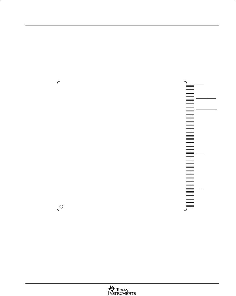
2.3.1Terminal Assignments for the GHH Package
See Table 2−2 for a description of each terminal’s function(s).
P |
XZCS0AND1 PWM8 |
PWM10 |
VSS |
VDD |
CAP6 |
XD[8] |
VSS |
VDD |
T3CTRIP |
T4CTRIP/ |
VDD |
XZCS2 |
SCITXDB |
||
_QEPI2 |
_PDPINTB EVBSOC |
||||||||||||||
|
|
|
|
|
|
|
|
|
|
|
|
||||
N |
SPISOMIA |
PWM7 |
PWM9 |
XR/W |
T4PWM |
C4TRIP |
TEST2 |
VDD3VFL |
XD[11] |
XA[2] |
XWE |
CANTXA |
CANRXA |
VDDIO |
|
_T4CMP |
|||||||||||||||
|
|
|
|
|
|
|
|
|
|
|
|
|
|
||
M |
SPISIMOA |
XA[1] |
XRD |
PWM12 |
CAP4 |
CAP5 |
TEST1 |
XD[9] |
X2 |
VSS |
XA[3] |
PWM1 |
SCIRXDB |
PWM2 |
|
_QEP3 |
_QEP4 |
||||||||||||||
|
|
|
|
|
|
|
|
|
|
|
|
|
|||
L |
VDD |
VSS |
XD[6] |
PWM11 |
XD[7] |
C5TRIP |
VDDIO |
TDIRB |
XD[10] |
VDDIO |
VSS |
PWM3 |
PWM4 |
XD[12] |
|
K |
VSS |
SPICLKA |
XD[4] |
SPISTEA |
T3PWM |
VSS |
C6TRIP |
TCLKINB |
X1/ |
XHOLDA |
PWM5 |
VDD |
VSS |
PWM6 |
|
_T3CMP |
XCLKIN |
||||||||||||||
|
|
|
|
|
|
|
|
|
|
|
|
|
|||
J |
MCLKXA |
MFSRA |
XD[3] |
VDDIO |
XD[5] |
|
|
|
|
XD[13] |
T1PWM |
XA[4] |
T2PWM |
VSS |
|
|
|
|
|
_T1CMP |
_T2CMP |
||||||||||
|
|
|
|
|
|
|
|
|
|
|
|
|
|||
H |
VDD |
MCLKRA |
XD[1] |
MFSXA |
XD[2] |
|
|
|
|
CAP1 |
CAP2 |
CAP3 |
XA[5] |
T1CTRIP |
|
|
|
|
|
_QEP1 _QEP2 _QEPI1 |
_PDPINTA |
||||||||||
|
|
|
|
|
|
|
|
|
|
|
|||||
G |
MDXA |
MDRA |
XD[0] |
VSS |
XA[0] |
|
|
|
|
T2CTRIP/ |
VDDIO |
VDD |
VSS |
XA[6] |
|
|
|
|
|
EVASOC |
|||||||||||
F |
XMP/MC |
ADC- |
VSSA1 |
VDDA1 |
ADCINB7 |
|
|
|
|
C3TRIP |
XCLKOUT |
XA[7] |
TCLKINA |
TDIRA |
|
RESEXT |
|
|
|
|
|||||||||||
E |
AVDD- |
ADCREFP |
AVSS- |
ADCREFM ADCINA5 |
ADC- |
XHOLD |
XNMI |
VDDIO |
XA[13] |
C2TRIP |
XA[8] |
C1TRIP |
VSS |
||
REFBG |
REFBG |
BGREFIN |
_XINT13 |
||||||||||||
D |
ADCINB6 ADCINB5 ADCINB4 ADCINA1 ADCINA6 |
XRS |
XA[18] |
XINT2 |
XINT1 |
VSS |
EMU0 |
TDO |
TMS |
XA[9] |
|||||
_ADCSOC |
_XBIO |
||||||||||||||
|
|
|
|
|
|
|
|
|
|
|
|
|
|||
C |
ADCINB3 ADCINB0 ADCINB1 ADCINA2 |
VSSA2 |
VSS1 |
SCITXDA |
VDD |
EMU1 |
VSS |
XA[12] |
XA[10] |
TDI |
VDD |
||||
B |
ADCINB2 |
VDDAIO |
ADCLO |
ADCINA3 ADCINA7 |
XREADY |
XA[17] |
VSS |
XA[15] |
VDD |
XD[14] |
TRST |
XZCS6AND7 VSS |
|||
A |
|
VSSAIO |
ADCINA0 ADCINA4 |
VDDA2 |
VDD1 |
SCIRXDA |
XA[16] |
XD[15] |
XA[14] |
XF |
TCK |
TESTSEL |
XA[11] |
||
|
_XPLLDIS |
||||||||||||||
|
|
|
|
|
|
|
|
|
|
|
|
|
|
||
1 |
2 |
3 |
4 |
5 |
6 |
7 |
8 |
9 |
10 |
11 |
12 |
13 |
14 |
Figure 2−1. TMS320F2812 and TMS320C2812 179-Ball GHH MicroStar BGA (Bottom View)
16 |
SPRS174M |
April 2001 − Revised October 2005 |
Introduction
2.3.2Pin Assignments for the PGF Package
The TMS320F2812 and TMS320C2812 176-pin PGF low-profile quad flatpack (LQFP) pin assignments are shown in Figure 2−2. See Table 2−2 for a description of each pin’s function(s).
|
|
|
|
|
|
|
|
|
|
XA[11] |
TDI |
XA[10] |
V |
V |
TDO |
TMS |
XA[9] |
|
C3TRIP |
|
C1TRIP |
XA[8] |
V |
XCLKOUT |
|
XA[7] |
TCLKINA |
TDIRA |
|
T2CTRIP/ EVASOC |
V |
V |
V |
XA[6] |
T1CTRIPPDPINTA |
CAP3QEPI1 |
XA[5] |
CAP2QEP2 |
CAP1QEP1 |
V |
T2PWMT2CMP |
XA[4] |
T1PWMT1CMP |
PWM6 |
V |
V |
PWM5 |
XD[13] |
XD[12] |
PWM4 |
PWM3 |
PWM2 |
PWM1 |
SCIRXDB |
SCITXDB |
|
CANRXA |
|||||||||||||||||||||||||||||||||||||||||||||||||||||||||||||||||||||||
|
|
|
|
|
|
|
|
|
|
|
|
|
|
|
|
|||||||||||||||||||||||||||||||||||||||||||||||||||||||||||||||||||||||||||||||||||||||||||||||||||||||||||||||||
|
|
|
|
|
|
|
|
|
|
|
|
|
|
|
|
|||||||||||||||||||||||||||||||||||||||||||||||||||||||||||||||||||||||||||||||||||||||||||||||||||||||||||||||||
|
|
|
|
|
|
|
|
|
|
|
|
|
|
|
||||||||||||||||||||||||||||||||||||||||||||||||||||||||||||||||||||||||||||||||||||||||||||||||||||||||||||||||||
|
|
|
|
|
|
|
|
|
|
|
C2TRIP |
|
|
|
||||||||||||||||||||||||||||||||||||||||||||||||||||||||||||||||||||||||||||||||||||||||||||||||||||||||||||||||||
|
|
|
|
|
|
|
|
|
|
|
|
|
|
|
|
|
|
|
SS DD |
|
|
|
|
|
|
|
|
|
|
|
|
|
|
|
|
|
|
|
SS |
|
|
|
|
|
|
|
|
|
|
|
|
|
|
|
DDIO |
|
SS DD |
|
|
|
|
|
|
|
|
|
|
|
|
|
|
|
|
SS |
|
|
|
|
|
|
|
|
|
|
|
|
DD SS |
|
|
|
|
|
|
|
|
|
|
|
|
|
|
|
|
|
|
|
|
|
|
|
|
|
|
|
||||||||||||||
|
|
|
|
|
132 |
|
|
|
|
|
|
|
|
|
|
|
|
|
|
|
|
|
|
|
|
|
|
|
|
|
|
|
|
|
|
|
|
|
|
|
|
|
|
|
|
|
|
|
|
|
|
|
|
|
|
|
|
|
|
|
|
|
|
|
|
|
|
|
|
|
|
|
|
|
|
|
|
|
|
|
|
|
|
|
|
|
|
|
|
|
|
|
|
|
|
|
|
|
|
|
|
|
|
|
|
|
|
|
|
|
|
|
|
|
|
|
|
|
|
|
|
89 |
||||||
|
|
|
|
|
|
|
|
|
|
|
|
|
|
|
|
|
|
|
|
|
|
|
|
|
|
|
|
|
|
|
|
|
|
|
|
|
|
|
|
|
|
|
|
|
|
|
|
|
|
|
|
|
|
|
|
|
|
|
|
|
|
|
|
|
|
|
|
|
|
|
|
|
|
|
|
|
|
|
|
|
|
|
|
|
|
|
|
|
|
|
|
|
|
|
|
|
|
|
|
|
|
|
|
|
|
|
|
|
|
|
|
|
|
|
|
|
|
|
|
|
||||||||
|
|
|
|
|
133 |
|
|
|
|
|
|
|
|
|
|
|
|
|
|
|
|
|
|
|
|
|
|
|
|
|
|
|
|
|
|
|
|
|
|
|
|
|
|
|
|
|
|
|
|
|
|
|
|
|
|
|
|
|
|
|
|
|
|
|
|
|
|
|
|
|
|
|
|
|
|
|
|
|
|
|
|
|
|
|
|
|
|
|
|
|
|
|
|
|
|
|
|
|
|
|
|
|
|
|
|
|
|
|
|
|
|
|
|
|
|
|
|
|
|
|
|
|
|
|
|
|
||
|
|
|
|
|
|
|
|
|
|
|
|
|
|
|
|
|
|
|
|
|
|
|
|
|
|
|
|
|
|
|
|
|
|
|
|
|
|
|
|
|
|
|
|
|
|
|
|
|
|
|
|
|
|
|
|
|
|
|
|
|
|
|
|
|
|
|
|
|
|
|
|
|
|
|
|
|
|
|
|
|
|
|
|
|
|
|
|
|
|
|
|
|
|
|
|
|
|
|
|
|
|
|
|
|
|
|
|
|
|
|
|
|
|
|
|
|
|
|
|
|
|
|
|
|
|
|||
|
|
|
|
|
|
|
|
|
|
131 |
130 |
129 |
128 |
127 |
126 |
125 |
124 |
123 |
122 |
121 |
120 |
119 |
118 |
117 |
116 |
115 |
114 |
113 |
112 |
111 |
110 |
109 |
108 |
107 |
106 |
105 |
104 |
103 |
102 |
101 |
100 |
99 |
98 |
97 |
96 |
95 |
94 |
93 |
92 |
91 |
90 |
|
|
|
|
|||||||||||||||||||||||||||||||||||||||||||||||||||||||||||||||||||||||||
|
|
|
|
|
|
|
|
|
|
|||||||||||||||||||||||||||||||||||||||||||||||||||||||||||||||||||||||||||||||||||||||||||||||||||||||||||||||||||||||
XZCS6AND7 |
|
|
|
|
|
|
|
|
|
|
|
|
||||||||||||||||||||||||||||||||||||||||||||||||||||||||||||||||||||||||||||||||||||||||||||||||||||||||||||||||||||
|
|
|
|
|
|
|
|
|
|
|
|
|
|
|
|
|
|
|
|
|
|
|
|
|
|
|
|
|
|
|
|
|
|
|
|
|
|
|
|
|
|
|
|
|
|
|
|
|
|
|
|
|
|
|
|
|
|
|
|
|
|
|
|
|
|
|
|
|
|
|
|
|
|
|
|
|
|
|
|
|
|
|
|
|
|
|
|
|
|
|
|
|
|
|
|
|
|
|
|
|
|
|
|
|
|
|
|
|
|
|
|
|
|
|
|
|
|
|
|
|
|
|
|
|||||
|
TESTSEL |
|
|
|
|
134 |
|
|
|
|
|
|
|
|
|
|
|
|
|
|
|
|
|
|
|
|
|
|
|
|
|
|
|
|
|
|
|
|
|
|
|
|
|
|
|
|
|
|
|
|
|
|
|
|
|
|
|
|
|
|
|
|
|
|
|
|
|
|
|
|
|
|
|
|
|
|
|
|
|
|
|
|
|
|
|
|
|
|
|
|
|
|
|
|
|
|
|
|
|
|
|
|
|
|
|
|
|
|
|
|
|
|
|
|
|
|
|
|
|
87 |
||||||||
|
|
|
|
|
|
|
|
|
|
|
|
|
|
|
|
|
|
|
|
|
|
|
|
|
|
|
|
|
|
|
|
|
|
|
|
|
|
|
|
|
|
|
|
|
|
|
|
|
|
|
|
|
|
|
|
|
|
|
|
|
|
|
|
|
|
|
|
|
|
|
|
|
|
|
|
|
|
|
|
|
|
|
|
|
|
|
|
|
|
|
|
|
|
|
|
|
|
|
|
|
|
|
|
|
|
|
|
|
|
|
|
|
|
|
|
|
||||||||||||
|
|
TRST |
|
|
|
|
135 |
|
|
|
|
|
|
|
|
|
|
|
|
|
|
|
|
|
|
|
|
|
|
|
|
|
|
|
|
|
|
|
|
|
|
|
|
|
|
|
|
|
|
|
|
|
|
|
|
|
|
|
|
|
|
|
|
|
|
|
|
|
|
|
|
|
|
|
|
|
|
|
|
|
|
|
|
|
|
|
|
|
|
|
|
|
|
|
|
|
|
|
|
|
|
|
|
|
|
|
|
|
|
|
|
|
|
|
|
|
|
|
|
|
86 |
|||||||
|
|
|
|
|
|
|
|
|
|
|
|
|
|
|
|
|
|
|
|
|
|
|
|
|
|
|
|
|
|
|
|
|
|
|
|
|
|
|
|
|
|
|
|
|
|
|
|
|
|
|
|
|
|
|
|
|
|
|
|
|
|
|
|
|
|
|
|
|
|
|
|
|
|
|
|
|
|
|
|
|
|
|
|
|
|
|
|
|
|
|
|
|
|
|
|
|
|
|
|
|
|
|
|
|
|
|
|
|
|
|
|
|
|
|
|
|
||||||||||||
|
|
TCK |
|
|
|
|
136 |
|
|
|
|
|
|
|
|
|
|
|
|
|
|
|
|
|
|
|
|
|
|
|
|
|
|
|
|
|
|
|
|
|
|
|
|
|
|
|
|
|
|
|
|
|
|
|
|
|
|
|
|
|
|
|
|
|
|
|
|
|
|
|
|
|
|
|
|
|
|
|
|
|
|
|
|
|
|
|
|
|
|
|
|
|
|
|
|
|
|
|
|
|
|
|
|
|
|
|
|
|
|
|
|
|
|
|
|
|
|
|
|
|
85 |
|||||||
|
|
|
|
|
|
|
|
|
|
|
|
|
|
|
|
|
|
|
|
|
|
|
|
|
|
|
|
|
|
|
|
|
|
|
|
|
|
|
|
|
|
|
|
|
|
|
|
|
|
|
|
|
|
|
|
|
|
|
|
|
|
|
|
|
|
|
|
|
|
|
|
|
|
|
|
|
|
|
|
|
|
|
|
|
|
|
|
|
|
|
|
|
|
|
|
|
|
|
|
|
|
|
|
|
|
|
|
|
|
|
|
|
|
|
|
|
||||||||||||
|
|
EMU0 |
|
|
|
|
137 |
|
|
|
|
|
|
|
|
|
|
|
|
|
|
|
|
|
|
|
|
|
|
|
|
|
|
|
|
|
|
|
|
|
|
|
|
|
|
|
|
|
|
|
|
|
|
|
|
|
|
|
|
|
|
|
|
|
|
|
|
|
|
|
|
|
|
|
|
|
|
|
|
|
|
|
|
|
|
|
|
|
|
|
|
|
|
|
|
|
|
|
|
|
|
|
|
|
|
|
|
|
|
|
|
|
|
|
|
|
|
|
|
|
84 |
|||||||
|
|
|
|
|
|
|
|
|
|
|
|
|
|
|
|
|
|
|
|
|
|
|
|
|
|
|
|
|
|
|
|
|
|
|
|
|
|
|
|
|
|
|
|
|
|
|
|
|
|
|
|
|
|
|
|
|
|
|
|
|
|
|
|
|
|
|
|
|
|
|
|
|
|
|
|
|
|
|
|
|
|
|
|
|
|
|
|
|
|
|
|
|
|
|
|
|
|
|
|
|
|
|
|
|
|
|
|
|
|
|
|
|
|
|
|
|
||||||||||||
|
|
XA[12] |
|
|
|
|
138 |
|
|
|
|
|
|
|
|
|
|
|
|
|
|
|
|
|
|
|
|
|
|
|
|
|
|
|
|
|
|
|
|
|
|
|
|
|
|
|
|
|
|
|
|
|
|
|
|
|
|
|
|
|
|
|
|
|
|
|
|
|
|
|
|
|
|
|
|
|
|
|
|
|
|
|
|
|
|
|
|
|
|
|
|
|
|
|
|
|
|
|
|
|
|
|
|
|
|
|
|
|
|
|
|
|
|
|
|
|
|
|
|
|
83 |
|||||||
|
|
|
|
|
|
|
|
|
|
|
|
|
|
|
|
|
|
|
|
|
|
|
|
|
|
|
|
|
|
|
|
|
|
|
|
|
|
|
|
|
|
|
|
|
|
|
|
|
|
|
|
|
|
|
|
|
|
|
|
|
|
|
|
|
|
|
|
|
|
|
|
|
|
|
|
|
|
|
|
|
|
|
|
|
|
|
|
|
|
|
|
|
|
|
|
|
|
|
|
|
|
|
|
|
|
|
|
|
|
|
|
|
|
|
|
|
||||||||||||
|
|
XD[14] |
|
|
|
|
139 |
|
|
|
|
|
|
|
|
|
|
|
|
|
|
|
|
|
|
|
|
|
|
|
|
|
|
|
|
|
|
|
|
|
|
|
|
|
|
|
|
|
|
|
|
|
|
|
|
|
|
|
|
|
|
|
|
|
|
|
|
|
|
|
|
|
|
|
|
|
|
|
|
|
|
|
|
|
|
|
|
|
|
|
|
|
|
|
|
|
|
|
|
|
|
|
|
|
|
|
|
|
|
|
|
|
|
|
|
|
|
|
|
|
82 |
|||||||
|
|
|
|
|
|
|
|
|
|
|
|
|
|
|
|
|
|
|
|
|
|
|
|
|
|
|
|
|
|
|
|
|
|
|
|
|
|
|
|
|
|
|
|
|
|
|
|
|
|
|
|
|
|
|
|
|
|
|
|
|
|
|
|
|
|
|
|
|
|
|
|
|
|
|
|
|
|
|
|
|
|
|
|
|
|
|
|
|
|
|
|
|
|
|
|
|
|
|
|
|
|
|
|
|
|
|
|
|
|
|
|
|
|
|
|
|
||||||||||||
XF_ |
XPLLDIS |
|
|
|
|
|
140 |
|
|
|
|
|
|
|
|
|
|
|
|
|
|
|
|
|
|
|
|
|
|
|
|
|
|
|
|
|
|
|
|
|
|
|
|
|
|
|
|
|
|
|
|
|
|
|
|
|
|
|
|
|
|
|
|
|
|
|
|
|
|
|
|
|
|
|
|
|
|
|
|
|
|
|
|
|
|
|
|
|
|
|
|
|
|
|
|
|
|
|
|
|
|
|
|
|
|
|
|
|
|
|
|
|
|
|
|
|
|
|
|
|
81 |
|||||||
|
|
|
|
|
|
|
|
|
|
|
|
|
|
|
|
|
|
|
|
|
|
|
|
|
|
|
|
|
|
|
|
|
|
|
|
|
|
|
|
|
|
|
|
|
|
|
|
|
|
|
|
|
|
|
|
|
|
|
|
|
|
|
|
|
|
|
|
|
|
|
|
|
|
|
|
|
|
|
|
|
|
|
|
|
|
|
|
|
|
|
|
|
|
|
|
|
|
|
|
|
|
|
|
|
|
|
|
|
|
|
|
|
|
|
|
|
||||||||||||
|
|
XA[13] |
|
|
|
|
141 |
|
|
|
|
|
|
|
|
|
|
|
|
|
|
|
|
|
|
|
|
|
|
|
|
|
|
|
|
|
|
|
|
|
|
|
|
|
|
|
|
|
|
|
|
|
|
|
|
|
|
|
|
|
|
|
|
|
|
|
|
|
|
|
|
|
|
|
|
|
|
|
|
|
|
|
|
|
|
|
|
|
|
|
|
|
|
|
|
|
|
|
|
|
|
|
|
|
|
|
|
|
|
|
|
|
|
|
|
|
|
|
|
|
80 |
|||||||
|
|
|
|
|
|
|
|
|
|
|
|
|
|
|
|
|
|
|
|
|
|
|
|
|
|
|
|
|
|
|
|
|
|
|
|
|
|
|
|
|
|
|
|
|
|
|
|
|
|
|
|
|
|
|
|
|
|
|
|
|
|
|
|
|
|
|
|
|
|
|
|
|
|
|
|
|
|
|
|
|
|
|
|
|
|
|
|
|
|
|
|
|
|
|
|
|
|
|
|
|
|
|
|
|
|
|
|
|
|
|
|
|
|
|
|
|
||||||||||||
|
|
VSS |
|
|
|
|
142 |
|
|
|
|
|
|
|
|
|
|
|
|
|
|
|
|
|
|
|
|
|
|
|
|
|
|
|
|
|
|
|
|
|
|
|
|
|
|
|
|
|
|
|
|
|
|
|
|
|
|
|
|
|
|
|
|
|
|
|
|
|
|
|
|
|
|
|
|
|
|
|
|
|
|
|
|
|
|
|
|
|
|
|
|
|
|
|
|
|
|
|
|
|
|
|
|
|
|
|
|
|
|
|
|
|
|
|
|
|
|
|
|
|
79 |
|||||||
|
|
|
|
|
|
|
|
|
|
|
|
|
|
|
|
|
|
|
|
|
|
|
|
|
|
|
|
|
|
|
|
|
|
|
|
|
|
|
|
|
|
|
|
|
|
|
|
|
|
|
|
|
|
|
|
|
|
|
|
|
|
|
|
|
|
|
|
|
|
|
|
|
|
|
|
|
|
|
|
|
|
|
|
|
|
|
|
|
|
|
|
|
|
|
|
|
|
|
|
|
|
|
|
|
|
|
|
|
|
|
|
|
|
|
|
|
||||||||||||
|
|
VDD |
|
|
|
|
143 |
|
|
|
|
|
|
|
|
|
|
|
|
|
|
|
|
|
|
|
|
|
|
|
|
|
|
|
|
|
|
|
|
|
|
|
|
|
|
|
|
|
|
|
|
|
|
|
|
|
|
|
|
|
|
|
|
|
|
|
|
|
|
|
|
|
|
|
|
|
|
|
|
|
|
|
|
|
|
|
|
|
|
|
|
|
|
|
|
|
|
|
|
|
|
|
|
|
|
|
|
|
|
|
|
|
|
|
|
|
|
|
|
|
78 |
|||||||
|
|
|
|
|
|
|
|
|
|
|
|
|
|
|
|
|
|
|
|
|
|
|
|
|
|
|
|
|
|
|
|
|
|
|
|
|
|
|
|
|
|
|
|
|
|
|
|
|
|
|
|
|
|
|
|
|
|
|
|
|
|
|
|
|
|
|
|
|
|
|
|
|
|
|
|
|
|
|
|
|
|
|
|
|
|
|
|
|
|
|
|
|
|
|
|
|
|
|
|
|
|
|
|
|
|
|
|
|
|
|
|
|
|
|
|
|
||||||||||||
|
|
XA[14] |
|
|
|
|
144 |
|
|
|
|
|
|
|
|
|
|
|
|
|
|
|
|
|
|
|
|
|
|
|
|
|
|
|
|
|
|
|
|
|
|
|
|
|
|
|
|
|
|
|
|
|
|
|
|
|
|
|
|
|
|
|
|
|
|
|
|
|
|
|
|
|
|
|
|
|
|
|
|
|
|
|
|
|
|
|
|
|
|
|
|
|
|
|
|
|
|
|
|
|
|
|
|
|
|
|
|
|
|
|
|
|
|
|
|
|
|
|
|
|
77 |
|||||||
|
|
|
|
|
|
|
|
|
|
|
|
|
|
|
|
|
|
|
|
|
|
|
|
|
|
|
|
|
|
|
|
|
|
|
|
|
|
|
|
|
|
|
|
|
|
|
|
|
|
|
|
|
|
|
|
|
|
|
|
|
|
|
|
|
|
|
|
|
|
|
|
|
|
|
|
|
|
|
|
|
|
|
|
|
|
|
|
|
|
|
|
|
|
|
|
|
|
|
|
|
|
|
|
|
|
|
|
|
|
|
|
|
|
|
|
|
||||||||||||
|
|
VDDIO |
|
|
|
|
145 |
|
|
|
|
|
|
|
|
|
|
|
|
|
|
|
|
|
|
|
|
|
|
|
|
|
|
|
|
|
|
|
|
|
|
|
|
|
|
|
|
|
|
|
|
|
|
|
|
|
|
|
|
|
|
|
|
|
|
|
|
|
|
|
|
|
|
|
|
|
|
|
|
|
|
|
|
|
|
|
|
|
|
|
|
|
|
|
|
|
|
|
|
|
|
|
|
|
|
|
|
|
|
|
|
|
|
|
|
|
|
|
|
|
76 |
|||||||
|
|
|
|
|
|
|
|
|
|
|
|
|
|
|
|
|
|
|
|
|
|
|
|
|
|
|
|
|
|
|
|
|
|
|
|
|
|
|
|
|
|
|
|
|
|
|
|
|
|
|
|
|
|
|
|
|
|
|
|
|
|
|
|
|
|
|
|
|
|
|
|
|
|
|
|
|
|
|
|
|
|
|
|
|
|
|
|
|
|
|
|
|
|
|
|
|
|
|
|
|
|
|
|
|
|
|
|
|
|
|
|
|
|
|
|
|
||||||||||||
|
|
EMU1 |
|
|
|
|
146 |
|
|
|
|
|
|
|
|
|
|
|
|
|
|
|
|
|
|
|
|
|
|
|
|
|
|
|
|
|
|
|
|
|
|
|
|
|
|
|
|
|
|
|
|
|
|
|
|
|
|
|
|
|
|
|
|
|
|
|
|
|
|
|
|
|
|
|
|
|
|
|
|
|
|
|
|
|
|
|
|
|
|
|
|
|
|
|
|
|
|
|
|
|
|
|
|
|
|
|
|
|
|
|
|
|
|
|
|
|
|
|
|
|
75 |
|||||||
|
|
|
|
|
|
|
|
|
|
|
|
|
|
|
|
|
|
|
|
|
|
|
|
|
|
|
|
|
|
|
|
|
|
|
|
|
|
|
|
|
|
|
|
|
|
|
|
|
|
|
|
|
|
|
|
|
|
|
|
|
|
|
|
|
|
|
|
|
|
|
|
|
|
|
|
|
|
|
|
|
|
|
|
|
|
|
|
|
|
|
|
|
|
|
|
|
|
|
|
|
|
|
|
|
|
|
|
|
|
|
|
|
|
|
|
|
||||||||||||
|
|
XD[15] |
|
|
|
|
147 |
|
|
|
|
|
|
|
|
|
|
|
|
|
|
|
|
|
|
|
|
|
|
|
|
|
|
|
|
|
|
|
|
|
|
|
|
|
|
|
|
|
|
|
|
|
|
|
|
|
|
|
|
|
|
|
|
|
|
|
|
|
|
|
|
|
|
|
|
|
|
|
|
|
|
|
|
|
|
|
|
|
|
|
|
|
|
|
|
|
|
|
|
|
|
|
|
|
|
|
|
|
|
|
|
|
|
|
|
|
|
|
|
|
74 |
|||||||
|
|
|
|
|
|
|
|
|
|
|
|
|
|
|
|
|
|
|
|
|
|
|
|
|
|
|
|
|
|
|
|
|
|
|
|
|
|
|
|
|
|
|
|
|
|
|
|
|
|
|
|
|
|
|
|
|
|
|
|
|
|
|
|
|
|
|
|
|
|
|
|
|
|
|
|
|
|
|
|
|
|
|
|
|
|
|
|
|
|
|
|
|
|
|
|
|
|
|
|
|
|
|
|
|
|
|
|
|
|
|
|
|
|
|
|
|
||||||||||||
|
|
XA[15] |
|
|
|
|
148 |
|
|
|
|
|
|
|
|
|
|
|
|
|
|
|
|
|
|
|
|
|
|
|
|
|
|
|
|
|
|
|
|
|
|
|
|
|
|
|
|
|
|
|
|
|
|
|
|
|
|
|
|
|
|
|
|
|
|
|
|
|
|
|
|
|
|
|
|
|
|
|
|
|
|
|
|
|
|
|
|
|
|
|
|
|
|
|
|
|
|
|
|
|
|
|
|
|
|
|
|
|
|
|
|
|
|
|
|
|
|
|
|
|
73 |
|||||||
|
|
|
|
|
|
|
|
|
|
|
|
|
|
|
|
|
|
|
|
|
|
|
|
|
|
|
|
|
|
|
|
|
|
|
|
|
|
|
|
|
|
|
|
|
|
|
|
|
|
|
|
|
|
|
|
|
|
|
|
|
|
|
|
|
|
|
|
|
|
|
|
|
|
|
|
|
|
|
|
|
|
|
|
|
|
|
|
|
|
|
|
|
|
|
|
|
|
|
|
|
|
|
|
|
|
|
|
|
|
|
|
|
|
|
|
|
||||||||||||
|
XINT1_XBIO |
|
|
|
|
149 |
|
|
|
|
|
|
|
|
|
|
|
|
|
|
|
|
|
|
|
|
|
|
|
|
|
|
|
|
|
|
|
|
|
|
|
|
|
|
|
|
|
|
|
|
|
|
|
|
|
|
|
|
|
|
|
|
|
|
|
|
|
|
|
|
|
|
|
|
|
|
|
|
|
|
|
|
|
|
|
|
|
|
|
|
|
|
|
|
|
|
|
|
|
|
|
|
|
|
|
|
|
|
|
|
|
|
|
|
|
|
|
|
|
72 |
||||||||
|
|
|
|
|
|
|
|
|
|
|
|
|
|
|
|
|
|
|
|
|
|
|
|
|
|
|
|
|
|
|
|
|
|
|
|
|
|
|
|
|
|
|
|
|
|
|
|
|
|
|
|
|
|
|
|
|
|
|
|
|
|
|
|
|
|
|
|
|
|
|
|
|
|
|
|
|
|
|
|
|
|
|
|
|
|
|
|
|
|
|
|
|
|
|
|
|
|
|
|
|
|
|
|
|
|
|
|
|
|
|
|
|
|
|
|
|
||||||||||||
XNMI_XINT13 |
|
|
|
|
150 |
|
|
|
|
|
|
|
|
|
|
|
|
|
|
|
|
|
|
|
|
|
|
|
|
|
|
|
|
|
|
|
|
|
|
|
|
|
|
|
|
|
|
|
|
|
|
|
|
|
|
|
|
|
|
|
|
|
|
|
|
|
|
|
|
|
|
|
|
|
|
|
|
|
|
|
|
|
|
|
|
|
|
|
|
|
|
|
|
|
|
|
|
|
|
|
|
|
|
|
|
|
|
|
|
|
|
|
|
|
|
|
|
|
71 |
|||||||||
|
|
|
|
|
|
|
|
|
|
|
|
|
|
|
|
|
|
|
|
|
|
|
|
|
|
|
|
|
|
|
|
|
|
|
|
|
|
|
|
|
|
|
|
|
|
|
|
|
|
|
|
|
|
|
|
|
|
|
|
|
|
|
|
|
|
|
|
|
|
|
|
|
|
|
|
|
|
|
|
|
|
|
|
|
|
|
|
|
|
|
|
|
|
|
|
|
|
|
|
|
|
|
|
|
|
|
|
|
|
|
|
|
|
|
|
|
||||||||||||
XINT2_ADCSOC |
|
|
|
|
151 |
|
|
|
|
|
|
|
|
|
|
|
|
|
|
|
|
|
|
|
|
|
|
|
|
|
|
|
|
|
|
|
|
|
|
|
|
|
|
|
|
|
|
|
|
|
|
|
|
|
|
|
|
|
|
|
|
|
|
|
|
|
|
|
|
|
|
|
|
|
|
|
|
|
|
|
|
|
|
|
|
|
|
|
|
|
|
|
|
|
|
|
|
|
|
|
|
|
|
|
|
|
|
|
|
|
|
|
|
|
|
|
|
|
70 |
|||||||||
|
|
|
|
|
|
|
|
|
|
|
|
|
|
|
|
|
|
|
|
|
|
|
|
|
|
|
|
|
|
|
|
|
|
|
|
|
|
|
|
|
|
|
|
|
|
|
|
|
|
|
|
|
|
|
|
|
|
|
|
|
|
|
|
|
|
|
|
|
|
|
|
|
|
|
|
|
|
|
|
|
|
|
|
|
|
|
|
|
|
|
|
|
|
|
|
|
|
|
|
|
|
|
|
|
|
|
|
|
|
|
|
|
|
|
|
|
||||||||||||
|
|
XA[16] |
|
|
|
|
152 |
|
|
|
|
|
|
|
|
|
|
|
|
|
|
|
|
|
|
|
|
|
|
|
|
|
|
|
|
|
|
|
|
|
|
|
|
|
|
|
|
|
|
|
|
|
|
|
|
|
|
|
|
|
|
|
|
|
|
|
|
|
|
|
|
|
|
|
|
|
|
|
|
|
|
|
|
|
|
|
|
|
|
|
|
|
|
|
|
|
|
|
|
|
|
|
|
|
|
|
|
|
|
|
|
|
|
|
|
|
|
|
|
|
69 |
|||||||
|
|
|
|
|
|
|
|
|
|
|
|
|
|
|
|
|
|
|
|
|
|
|
|
|
|
|
|
|
|
|
|
|
|
|
|
|
|
|
|
|
|
|
|
|
|
|
|
|
|
|
|
|
|
|
|
|
|
|
|
|
|
|
|
|
|
|
|
|
|
|
|
|
|
|
|
|
|
|
|
|
|
|
|
|
|
|
|
|
|
|
|
|
|
|
|
|
|
|
|
|
|
|
|
|
|
|
|
|
|
|
|
|
|
|
|
|
||||||||||||
|
|
VSS |
|
|
|
|
153 |
|
|
|
|
|
|
|
|
|
|
|
|
|
|
|
|
|
|
|
|
|
|
|
|
|
|
|
|
|
|
|
|
|
|
|
|
|
|
|
|
|
|
|
|
|
|
|
|
|
|
|
|
|
|
|
|
|
|
|
|
|
|
|
|
|
|
|
|
|
|
|
|
|
|
|
|
|
|
|
|
|
|
|
|
|
|
|
|
|
|
|
|
|
|
|
|
|
|
|
|
|
|
|
|
|
|
|
|
|
|
|
|
|
68 |
|||||||
|
|
|
|
|
|
|
|
|
|
|
|
|
|
|
|
|
|
|
|
|
|
|
|
|
|
|
|
|
|
|
|
|
|
|
|
|
|
|
|
|
|
|
|
|
|
|
|
|
|
|
|
|
|
|
|
|
|
|
|
|
|
|
|
|
|
|
|
|
|
|
|
|
|
|
|
|
|
|
|
|
|
|
|
|
|
|
|
|
|
|
|
|
|
|
|
|
|
|
|
|
|
|
|
|
|
|
|
|
|
|
|
|
|
|
|
|
||||||||||||
|
|
VDD |
|
|
|
|
154 |
|
|
|
|
|
|
|
|
|
|
|
|
|
|
|
|
|
|
|
|
|
|
|
|
|
|
|
|
|
|
|
|
|
|
|
|
|
|
|
|
|
|
|
|
|
|
|
|
|
|
|
|
|
|
|
|
|
|
|
|
|
|
|
|
|
|
|
|
|
|
|
|
|
|
|
|
|
|
|
|
|
|
|
|
|
|
|
|
|
|
|
|
|
|
|
|
|
|
|
|
|
|
|
|
|
|
|
|
|
|
|
|
|
67 |
|||||||
|
|
|
|
|
|
|
|
|
|
|
|
|
|
|
|
|
|
|
|
|
|
|
|
|
|
|
|
|
|
|
|
|
|
|
|
|
|
|
|
|
|
|
|
|
|
|
|
|
|
|
|
|
|
|
|
|
|
|
|
|
|
|
|
|
|
|
|
|
|
|
|
|
|
|
|
|
|
|
|
|
|
|
|
|
|
|
|
|
|
|
|
|
|
|
|
|
|
|
|
|
|
|
|
|
|
|
|
|
|
|
|
|
|
|
|
|
||||||||||||
|
|
SCITXDA |
|
|
|
|
155 |
|
|
|
|
|
|
|
|
|
|
|
|
|
|
|
|
|
|
|
|
|
|
|
|
|
|
|
|
|
|
|
|
|
|
|
|
|
|
|
|
|
|
|
|
|
|
|
|
|
|
|
|
|
|
|
|
|
|
|
|
|
|
|
|
|
|
|
|
|
|
|
|
|
|
|
|
|
|
|
|
|
|
|
|
|
|
|
|
|
|
|
|
|
|
|
|
|
|
|
|
|
|
|
|
|
|
|
|
|
|
|
|
|
66 |
|||||||
|
|
|
|
|
|
|
|
|
|
|
|
|
|
|
|
|
|
|
|
|
|
|
|
|
|
|
|
|
|
|
|
|
|
|
|
|
|
|
|
|
|
|
|
|
|
|
|
|
|
|
|
|
|
|
|
|
|
|
|
|
|
|
|
|
|
|
|
|
|
|
|
|
|
|
|
|
|
|
|
|
|
|
|
|
|
|
|
|
|
|
|
|
|
|
|
|
|
|
|
|
|
|
|
|
|
|
|
|
|
|
|
|
|
|
|
|
||||||||||||
|
|
XA[17] |
|
|
|
|
156 |
|
|
|
|
|
|
|
|
|
|
|
|
|
|
|
|
|
|
|
|
|
|
|
|
|
|
|
|
|
|
|
|
|
|
|
|
|
|
|
|
|
|
|
|
|
|
|
|
|
|
|
|
|
|
|
|
|
|
|
|
|
|
|
|
|
|
|
|
|
|
|
|
|
|
|
|
|
|
|
|
|
|
|
|
|
|
|
|
|
|
|
|
|
|
|
|
|
|
|
|
|
|
|
|
|
|
|
|
|
|
|
|
|
65 |
|||||||
|
|
|
|
|
|
|
|
|
|
|
|
|
|
|
|
|
|
|
|
|
|
|
|
|
|
|
|
|
|
|
|
|
|
|
|
|
|
|
|
|
|
|
|
|
|
|
|
|
|
|
|
|
|
|
|
|
|
|
|
|
|
|
|
|
|
|
|
|
|
|
|
|
|
|
|
|
|
|
|
|
|
|
|
|
|
|
|
|
|
|
|
|
|
|
|
|
|
|
|
|
|
|
|
|
|
|
|
|
|
|
|
|
|
|
|
|
||||||||||||
|
|
SCIRXDA |
|
|
|
|
157 |
|
|
|
|
|
|
|
|
|
|
|
|
|
|
|
|
|
|
|
|
|
|
|
|
|
|
|
|
|
|
|
|
|
|
|
|
|
|
|
|
|
|
|
|
|
|
|
|
|
|
|
|
|
|
|
|
|
|
|
|
|
|
|
|
|
|
|
|
|
|
|
|
|
|
|
|
|
|
|
|
|
|
|
|
|
|
|
|
|
|
|
|
|
|
|
|
|
|
|
|
|
|
|
|
|
|
|
|
|
|
|
|
|
64 |
|||||||
|
|
|
|
|
|
|
|
|
|
|
|
|
|
|
|
|
|
|
|
|
|
|
|
|
|
|
|
|
|
|
|
|
|
|
|
|
|
|
|
|
|
|
|
|
|
|
|
|
|
|
|
|
|
|
|
|
|
|
|
|
|
|
|
|
|
|
|
|
|
|
|
|
|
|
|
|
|
|
|
|
|
|
|
|
|
|
|
|
|
|
|
|
|
|
|
|
|
|
|
|
|
|
|
|
|
|
|
|
|
|
|
|
|
|
|
|
||||||||||||
|
|
XA[18] |
|
|
|
|
158 |
|
|
|
|
|
|
|
|
|
|
|
|
|
|
|
|
|
|
|
|
|
|
|
|
|
|
|
|
|
|
|
|
|
|
|
|
|
|
|
|
|
|
|
|
|
|
|
|
|
|
|
|
|
|
|
|
|
|
|
|
|
|
|
|
|
|
|
|
|
|
|
|
|
|
|
|
|
|
|
|
|
|
|
|
|
|
|
|
|
|
|
|
|
|
|
|
|
|
|
|
|
|
|
|
|
|
|
|
|
|
|
|
|
63 |
|||||||
|
|
|
|
|
|
|
|
|
|
|
|
|
|
|
|
|
|
|
|
|
|
|
|
|
|
|
|
|
|
|
|
|
|
|
|
|
|
|
|
|
|
|
|
|
|
|
|
|
|
|
|
|
|
|
|
|
|
|
|
|
|
|
|
|
|
|
|
|
|
|
|
|
|
|
|
|
|
|
|
|
|
|
|
|
|
|
|
|
|
|
|
|
|
|
|
|
|
|
|
|
|
|
|
|
|
|
|
|
|
|
|
|
|
|
|
|
||||||||||||
|
|
XHOLD |
|
|
|
|
159 |
|
|
|
|
|
|
|
|
|
|
|
|
|
|
|
|
|
|
|
|
|
|
|
|
|
|
|
|
|
|
|
|
|
|
|
|
|
|
|
|
|
|
|
|
|
|
|
|
|
|
|
|
|
|
|
|
|
|
|
|
|
|
|
|
|
|
|
|
|
|
|
|
|
|
|
|
|
|
|
|
|
|
|
|
|
|
|
|
|
|
|
|
|
|
|
|
|
|
|
|
|
|
|
|
|
|
|
|
|
|
|
|
|
62 |
|||||||
|
|
|
|
|
|
|
|
|
|
|
|
|
|
|
|
|
|
|
|
|
|
|
|
|
|
|
|
|
|
|
|
|
|
|
|
|
|
|
|
|
|
|
|
|
|
|
|
|
|
|
|
|
|
|
|
|
|
|
|
|
|
|
|
|
|
|
|
|
|
|
|
|
|
|
|
|
|
|
|
|
|
|
|
|
|
|
|
|
|
|
|
|
|
|
|
|
|
|
|
|
|
|
|
|
|
|
|
|
|
|
|
|
|
|
|
|
||||||||||||
|
|
XRS |
|
|
|
|
160 |
|
|
|
|
|
|
|
|
|
|
|
|
|
|
|
|
|
|
|
|
|
|
|
|
|
|
|
|
|
|
|
|
|
|
|
|
|
|
|
|
|
|
|
|
|
|
|
|
|
|
|
|
|
|
|
|
|
|
|
|
|
|
|
|
|
|
|
|
|
|
|
|
|
|
|
|
|
|
|
|
|
|
|
|
|
|
|
|
|
|
|
|
|
|
|
|
|
|
|
|
|
|
|
|
|
|
|
|
|
|
|
|
|
61 |
|||||||
|
|
|
|
|
|
|
|
|
|
|
|
|
|
|
|
|
|
|
|
|
|
|
|
|
|
|
|
|
|
|
|
|
|
|
|
|
|
|
|
|
|
|
|
|
|
|
|
|
|
|
|
|
|
|
|
|
|
|
|
|
|
|
|
|
|
|
|
|
|
|
|
|
|
|
|
|
|
|
|
|
|
|
|
|
|
|
|
|
|
|
|
|
|
|
|
|
|
|
|
|
|
|
|
|
|
|
|
|
|
|
|
|
|
|
|
|
||||||||||||
|
|
XREADY |
|
|
|
|
161 |
|
|
|
|
|
|
|
|
|
|
|
|
|
|
|
|
|
|
|
|
|
|
|
|
|
|
|
|
|
|
|
|
|
|
|
|
|
|
|
|
|
|
|
|
|
|
|
|
|
|
|
|
|
|
|
|
|
|
|
|
|
|
|
|
|
|
|
|
|
|
|
|
|
|
|
|
|
|
|
|
|
|
|
|
|
|
|
|
|
|
|
|
|
|
|
|
|
|
|
|
|
|
|
|
|
|
|
|
|
|
|
|
|
60 |
|||||||
|
|
|
|
|
|
|
|
|
|
|
|
|
|
|
|
|
|
|
|
|
|
|
|
|
|
|
|
|
|
|
|
|
|
|
|
|
|
|
|
|
|
|
|
|
|
|
|
|
|
|
|
|
|
|
|
|
|
|
|
|
|
|
|
|
|
|
|
|
|
|
|
|
|
|
|
|
|
|
|
|
|
|
|
|
|
|
|
|
|
|
|
|
|
|
|
|
|
|
|
|
|
|
|
|
|
|
|
|
|
|
|
|
|
|
|
|
||||||||||||
|
|
VDD1 |
|
|
|
|
162 |
|
|
|
|
|
|
|
|
|
|
|
|
|
|
|
|
|
|
|
|
|
|
|
|
|
|
|
|
|
|
|
|
|
|
|
|
|
|
|
|
|
|
|
|
|
|
|
|
|
|
|
|
|
|
|
|
|
|
|
|
|
|
|
|
|
|
|
|
|
|
|
|
|
|
|
|
|
|
|
|
|
|
|
|
|
|
|
|
|
|
|
|
|
|
|
|
|
|
|
|
|
|
|
|
|
|
|
|
|
|
|
|
|
59 |
|||||||
|
|
|
|
|
|
|
|
|
|
|
|
|
|
|
|
|
|
|
|
|
|
|
|
|
|
|
|
|
|
|
|
|
|
|
|
|
|
|
|
|
|
|
|
|
|
|
|
|
|
|
|
|
|
|
|
|
|
|
|
|
|
|
|
|
|
|
|
|
|
|
|
|
|
|
|
|
|
|
|
|
|
|
|
|
|
|
|
|
|
|
|
|
|
|
|
|
|
|
|
|
|
|
|
|
|
|
|
|
|
|
|
|
|
|
|
|
||||||||||||
|
|
VSS1 |
|
|
|
|
163 |
|
|
|
|
|
|
|
|
|
|
|
|
|
|
|
|
|
|
|
|
|
|
|
|
|
|
|
|
|
|
|
|
|
|
|
|
|
|
|
|
|
|
|
|
|
|
|
|
|
|
|
|
|
|
|
|
|
|
|
|
|
|
|
|
|
|
|
|
|
|
|
|
|
|
|
|
|
|
|
|
|
|
|
|
|
|
|
|
|
|
|
|
|
|
|
|
|
|
|
|
|
|
|
|
|
|
|
|
|
|
|
|
|
58 |
|||||||
|
|
|
|
|
|
|
|
|
|
|
|
|
|
|
|
|
|
|
|
|
|
|
|
|
|
|
|
|
|
|
|
|
|
|
|
|
|
|
|
|
|
|
|
|
|
|
|
|
|
|
|
|
|
|
|
|
|
|
|
|
|
|
|
|
|
|
|
|
|
|
|
|
|
|
|
|
|
|
|
|
|
|
|
|
|
|
|
|
|
|
|
|
|
|
|
|
|
|
|
|
|
|
|
|
|
|
|
|
|
|
|
|
|
|
|
|
||||||||||||
ADCBGREFIN |
|
|
|
|
164 |
|
|
|
|
|
|
|
|
|
|
|
|
|
|
|
|
|
|
|
|
|
|
|
|
|
|
|
|
|
|
|
|
|
|
|
|
|
|
|
|
|
|
|
|
|
|
|
|
|
|
|
|
|
|
|
|
|
|
|
|
|
|
|
|
|
|
|
|
|
|
|
|
|
|
|
|
|
|
|
|
|
|
|
|
|
|
|
|
|
|
|
|
|
|
|
|
|
|
|
|
|
|
|
|
|
|
|
|
|
|
|
|
|
57 |
|||||||||
|
|
|
|
|
|
|
|
|
|
|
|
|
|
|
|
|
|
|
|
|
|
|
|
|
|
|
|
|
|
|
|
|
|
|
|
|
|
|
|
|
|
|
|
|
|
|
|
|
|
|
|
|
|
|
|
|
|
|
|
|
|
|
|
|
|
|
|
|
|
|
|
|
|
|
|
|
|
|
|
|
|
|
|
|
|
|
|
|
|
|
|
|
|
|
|
|
|
|
|
|
|
|
|
|
|
|
|
|
|
|
|
|
|
|
|
|
||||||||||||
|
|
VSSA2 |
|
|
|
|
165 |
|
|
|
|
|
|
|
|
|
|
|
|
|
|
|
|
|
|
|
|
|
|
|
|
|
|
|
|
|
|
|
|
|
|
|
|
|
|
|
|
|
|
|
|
|
|
|
|
|
|
|
|
|
|
|
|
|
|
|
|
|
|
|
|
|
|
|
|
|
|
|
|
|
|
|
|
|
|
|
|
|
|
|
|
|
|
|
|
|
|
|
|
|
|
|
|
|
|
|
|
|
|
|
|
|
|
|
|
|
|
|
|
|
56 |
|||||||
|
|
|
|
|
|
|
|
|
|
|
|
|
|
|
|
|
|
|
|
|
|
|
|
|
|
|
|
|
|
|
|
|
|
|
|
|
|
|
|
|
|
|
|
|
|
|
|
|
|
|
|
|
|
|
|
|
|
|
|
|
|
|
|
|
|
|
|
|
|
|
|
|
|
|
|
|
|
|
|
|
|
|
|
|
|
|
|
|
|
|
|
|
|
|
|
|
|
|
|
|
|
|
|
|
|
|
|
|
|
|
|
|
|
|
|
|
||||||||||||
|
|
VDDA2 |
|
|
|
|
166 |
|
|
|
|
|
|
|
|
|
|
|
|
|
|
|
|
|
|
|
|
|
|
|
|
|
|
|
|
|
|
|
|
|
|
|
|
|
|
|
|
|
|
|
|
|
|
|
|
|
|
|
|
|
|
|
|
|
|
|
|
|
|
|
|
|
|
|
|
|
|
|
|
|
|
|
|
|
|
|
|
|
|
|
|
|
|
|
|
|
|
|
|
|
|
|
|
|
|
|
|
|
|
|
|
|
|
|
|
|
|
|
|
|
55 |
|||||||
|
|
|
|
|
|
|
|
|
|
|
|
|
|
|
|
|
|
|
|
|
|
|
|
|
|
|
|
|
|
|
|
|
|
|
|
|
|
|
|
|
|
|
|
|
|
|
|
|
|
|
|
|
|
|
|
|
|
|
|
|
|
|
|
|
|
|
|
|
|
|
|
|
|
|
|
|
|
|
|
|
|
|
|
|
|
|
|
|
|
|
|
|
|
|
|
|
|
|
|
|
|
|
|
|
|
|
|
|
|
|
|
|
|
|
|
|
||||||||||||
|
|
ADCINA7 |
|
|
|
|
167 |
|
|
|
|
|
|
|
|
|
|
|
|
|
|
|
|
|
|
|
|
|
|
|
|
|
|
|
|
|
|
|
|
|
|
|
|
|
|
|
|
|
|
|
|
|
|
|
|
|
|
|
|
|
|
|
|
|
|
|
|
|
|
|
|
|
|
|
|
|
|
|
|
|
|
|
|
|
|
|
|
|
|
|
|
|
|
|
|
|
|
|
|
|
|
|
|
|
|
|
|
|
|
|
|
|
|
|
|
|
|
|
|
|
54 |
|||||||
|
|
|
|
|
|
|
|
|
|
|
|
|
|
|
|
|
|
|
|
|
|
|
|
|
|
|
|
|
|
|
|
|
|
|
|
|
|
|
|
|
|
|
|
|
|
|
|
|
|
|
|
|
|
|
|
|
|
|
|
|
|
|
|
|
|
|
|
|
|
|
|
|
|
|
|
|
|
|
|
|
|
|
|
|
|
|
|
|
|
|
|
|
|
|
|
|
|
|
|
|
|
|
|
|
|
|
|
|
|
|
|
|
|
|
|
|
||||||||||||
|
|
ADCINA6 |
|
|
|
|
168 |
|
|
|
|
|
|
|
|
|
|
|
|
|
|
|
|
|
|
|
|
|
|
|
|
|
|
|
|
|
|
|
|
|
|
|
|
|
|
|
|
|
|
|
|
|
|
|
|
|
|
|
|
|
|
|
|
|
|
|
|
|
|
|
|
|
|
|
|
|
|
|
|
|
|
|
|
|
|
|
|
|
|
|
|
|
|
|
|
|
|
|
|
|
|
|
|
|
|
|
|
|
|
|
|
|
|
|
|
|
|
|
|
|
53 |
|||||||
|
|
|
|
|
|
|
|
|
|
|
|
|
|
|
|
|
|
|
|
|
|
|
|
|
|
|
|
|
|
|
|
|
|
|
|
|
|
|
|
|
|
|
|
|
|
|
|
|
|
|
|
|
|
|
|
|
|
|
|
|
|
|
|
|
|
|
|
|
|
|
|
|
|
|
|
|
|
|
|
|
|
|
|
|
|
|
|
|
|
|
|
|
|
|
|
|
|
|
|
|
|
|
|
|
|
|
|
|
|
|
|
|
|
|
|
|
||||||||||||
|
|
ADCINA5 |
|
|
|
|
169 |
|
|
|
|
|
|
|
|
|
|
|
|
|
|
|
|
|
|
|
|
|
|
|
|
|
|
|
|
|
|
|
|
|
|
|
|
|
|
|
|
|
|
|
|
|
|
|
|
|
|
|
|
|
|
|
|
|
|
|
|
|
|
|
|
|
|
|
|
|
|
|
|
|
|
|
|
|
|
|
|
|
|
|
|
|
|
|
|
|
|
|
|
|
|
|
|
|
|
|
|
|
|
|
|
|
|
|
|
|
|
|
|
|
52 |
|||||||
|
|
|
|
|
|
|
|
|
|
|
|
|
|
|
|
|
|
|
|
|
|
|
|
|
|
|
|
|
|
|
|
|
|
|
|
|
|
|
|
|
|
|
|
|
|
|
|
|
|
|
|
|
|
|
|
|
|
|
|
|
|
|
|
|
|
|
|
|
|
|
|
|
|
|
|
|
|
|
|
|
|
|
|
|
|
|
|
|
|
|
|
|
|
|
|
|
|
|
|
|
|
|
|
|
|
|
|
|
|
|
|
|
|
|
|
|
||||||||||||
|
ADCINA4 |
|
|
|
|
170 |
|
|
|
|
|
|
|
|
|
|
|
|
|
|
|
|
|
|
|
|
|
|
|
|
|
|
|
|
|
|
|
|
|
|
|
|
|
|
|
|
|
|
|
|
|
|
|
|
|
|
|
|
|
|
|
|
|
|
|
|
|
|
|
|
|
|
|
|
|
|
|
|
|
|
|
|
|
|
|
|
|
|
|
|
|
|
|
|
|
|
|
|
|
|
|
|
|
|
|
|
|
|
|
|
|
|
|
|
|
|
|
|
|
51 |
||||||||
|
|
|
|
|
|
|
|
|
|
|
|
|
|
|
|
|
|
|
|
|
|
|
|
|
|
|
|
|
|
|
|
|
|
|
|
|
|
|
|
|
|
|
|
|
|
|
|
|
|
|
|
|
|
|
|
|
|
|
|
|
|
|
|
|
|
|
|
|
|
|
|
|
|
|
|
|
|
|
|
|
|
|
|
|
|
|
|
|
|
|
|
|
|
|
|
|
|
|
|
|
|
|
|
|
|
|
|
|
|
|
|
|
|
|
|
|
||||||||||||
|
|
ADCINA3 |
|
|
|
|
171 |
|
|
|
|
|
|
|
|
|
|
|
|
|
|
|
|
|
|
|
|
|
|
|
|
|
|
|
|
|
|
|
|
|
|
|
|
|
|
|
|
|
|
|
|
|
|
|
|
|
|
|
|
|
|
|
|
|
|
|
|
|
|
|
|
|
|
|
|
|
|
|
|
|
|
|
|
|
|
|
|
|
|
|
|
|
|
|
|
|
|
|
|
|
|
|
|
|
|
|
|
|
|
|
|
|
|
|
|
|
|
|
|
|
50 |
|||||||
|
|
|
|
|
|
|
|
|
|
|
|
|
|
|
|
|
|
|
|
|
|
|
|
|
|
|
|
|
|
|
|
|
|
|
|
|
|
|
|
|
|
|
|
|
|
|
|
|
|
|
|
|
|
|
|
|
|
|
|
|
|
|
|
|
|
|
|
|
|
|
|
|
|
|
|
|
|
|
|
|
|
|
|
|
|
|
|
|
|
|
|
|
|
|
|
|
|
|
|
|
|
|
|
|
|
|
|
|
|
|
|
|
|
|
|
|
||||||||||||
|
|
ADCINA2 |
|
|
|
|
172 |
|
|
|
|
|
|
|
|
|
|
|
|
|
|
|
|
|
|
|
|
|
|
|
|
|
|
|
|
|
|
|
|
|
|
|
|
|
|
|
|
|
|
|
|
|
|
|
|
|
|
|
|
|
|
|
|
|
|
|
|
|
|
|
|
|
|
|
|
|
|
|
|
|
|
|
|
|
|
|
|
|
|
|
|
|
|
|
|
|
|
|
|
|
|
|
|
|
|
|
|
|
|
|
|
|
|
|
|
|
|
|
|
|
49 |
|||||||
|
|
|
|
|
|
|
|
|
|
|
|
|
|
|
|
|
|
|
|
|
|
|
|
|
|
|
|
|
|
|
|
|
|
|
|
|
|
|
|
|
|
|
|
|
|
|
|
|
|
|
|
|
|
|
|
|
|
|
|
|
|
|
|
|
|
|
|
|
|
|
|
|
|
|
|
|
|
|
|
|
|
|
|
|
|
|
|
|
|
|
|
|
|
|
|
|
|
|
|
|
|
|
|
|
|
|
|
|
|
|
|
|
|
|
|
|
||||||||||||
|
|
ADCINA1 |
|
|
|
|
173 |
|
|
|
|
|
|
|
|
|
|
|
|
|
|
|
|
|
|
|
|
|
|
|
|
|
|
|
|
|
|
|
|
|
|
|
|
|
|
|
|
|
|
|
|
|
|
|
|
|
|
|
|
|
|
|
|
|
|
|
|
|
|
|
|
|
|
|
|
|
|
|
|
|
|
|
|
|
|
|
|
|
|
|
|
|
|
|
|
|
|
|
|
|
|
|
|
|
|
|
|
|
|
|
|
|
|
|
|
|
|
|
|
|
48 |
|||||||
|
|
|
|
|
|
|
|
|
|
|
|
|
|
|
|
|
|
|
|
|
|
|
|
|
|
|
|
|
|
|
|
|
|
|
|
|
|
|
|
|
|
|
|
|
|
|
|
|
|
|
|
|
|
|
|
|
|
|
|
|
|
|
|
|
|
|
|
|
|
|
|
|
|
|
|
|
|
|
|
|
|
|
|
|
|
|
|
|
|
|
|
|
|
|
|
|
|
|
|
|
|
|
|
|
|
|
|
|
|
|
|
|
|
|
|
|
||||||||||||
|
|
ADCINA0 |
|
|
|
|
174 |
|
|
|
|
|
|
|
|
|
|
|
|
|
|
|
|
|
|
|
|
|
|
|
|
|
|
|
|
|
|
|
|
|
|
|
|
|
|
|
|
|
|
|
|
|
|
|
|
|
|
|
|
|
|
|
|
|
|
|
|
|
|
|
|
|
|
|
|
|
|
|
|
|
|
|
|
|
|
|
|
|
|
|
|
|
|
|
|
|
|
|
|
|
|
|
|
|
|
|
|
|
|
|
|
|
|
|
|
|
|
|
|
|
47 |
|||||||
|
|
|
|
|
|
|
|
|
|
|
|
|
|
|
|
|
|
|
|
|
|
|
|
|
|
|
|
|
|
|
|
|
|
|
|
|
|
|
|
|
|
|
|
|
|
|
|
|
|
|
|
|
|
|
|
|
|
|
|
|
|
|
|
|
|
|
|
|
|
|
|
|
|
|
|
|
|
|
|
|
|
|
|
|
|
|
|
|
|
|
|
|
|
|
|
|
|
|
|
|
|
|
|
|
|
|
|
|
|
|
|
|
|
|
|
|
||||||||||||
|
|
ADCLO |
|
|
|
|
175 |
|
|
|
|
|
|
|
|
|
|
|
|
|
|
|
|
|
|
|
|
|
|
|
|
|
|
|
|
|
|
|
|
|
|
|
|
|
|
|
|
|
|
|
|
|
|
|
|
|
|
|
|
|
|
|
|
|
|
|
|
|
|
|
|
|
|
|
|
|
|
|
|
|
|
|
|
|
|
|
|
|
|
|
|
|
|
|
|
|
|
|
|
|
|
|
|
|
|
|
|
|
|
|
|
|
|
|
|
|
|
|
|
|
46 |
|||||||
|
|
|
|
|
|
|
|
|
|
|
|
|
|
|
|
|
|
|
|
|
|
|
|
|
|
|
|
|
|
|
|
|
|
|
|
|
|
|
|
|
|
|
|
|
|
|
|
|
|
|
|
|
|
|
|
|
|
|
|
|
|
|
|
|
|
|
|
|
|
|
|
|
|
|
|
|
|
|
|
|
|
|
|
|
|
|
|
|
|
|
|
|
|
|
|
|
|
|
|
|
|
|
|
|
|
|
|
|
|
|
|
|
|
|
|
|
||||||||||||
|
|
VSSAIO |
|
|
|
|
|
|
|
|
2 |
3 4 |
5 6 |
7 8 |
9 |
10 |
11 |
12 |
13 |
14 |
15 |
16 |
17 |
18 |
19 |
20 |
21 |
22 23 |
24 25 |
26 27 |
28 29 |
30 |
31 |
32 |
33 |
34 |
35 |
36 |
37 |
38 |
39 |
40 41 |
42 43 |
|
|
|
|
|||||||||||||||||||||||||||||||||||||||||||||||||||||||||||||||||||||||||||||||||
176 |
|
|
|
|
|
|
|
|
|
|||||||||||||||||||||||||||||||||||||||||||||||||||||||||||||||||||||||||||||||||||||||||||||||||||||||||||||||||||||||
|
|
|
|
|
|
|
|
|
|
|
|
|
|
|
|
|
|
|
|
|
|
|
|
|
|
|
|
|
|
|
|
|
|
|
|
|
|
|
|
|
|
|
|
|
|
|
|
|
|
|
|
|
|
|
|
|
|
|
|
|
|
|
|
|
|
|
|
|
|
|
|
|
|
|
|
|
|
|
|
|
|
|
|
|
|
|
|
|
|
|
|
|
|
|
|
|
|
|
|
|
|
|
|
|
|
|
|
|
|
|
|
|
|
|
|
|
|
|
|
|
|
|
|
|
|
|||
|
|
|
|
|
1 |
|
|
|
|
|
|
|
|
|
|
|
|
|
|
|
|
|
|
|
|
|
|
|
|
|
|
|
|
|
|
|
|
|
|
|
|
|
|
|
|
|
|
|
|
|
|
|
|
|
|
|
|
|
|
|
|
|
|
|
|
|
|
|
|
|
|
|
|
|
|
|
|
|
|
|
|
|
|
|
|
|
|
|
|
|
|
|
|
|
|
|
|
|
|
|
|
|
|
|
|
|
|
|
|
|
|
|
|
|
|
|
|
|
|
|
|
44 |
||||||
|
|
|
|
|
|
|
|
|
|
|
|
|
|
|
|
|
|
|
|
|
|
|
|
|
|
|
|
|
|
|
|
|
|
|
|
|
|
|
|
|
|
|
|
|
|
|
|
|
|
|
|
|
|
|
|
|
|
|
|
|
|
|
|
|
|
|
|
|
|
|
|
|
|
|
|
|
|
|
|
|
|
|
|
|
|
|
|
|
|
|
|
|
|
|
|
|
|
|
|
|
|
|
|
|
|
|
|
|
|
|
|
|
|
|
|
|
|
|
|
|
||||||||
|
|
|
|
|
|
|
|
|
|
V |
ADCINB0 |
ADCINB1 |
ADCINB2 |
|
ADCINB3 |
ADCINB4 |
ADCINB5 |
ADCINB6 |
|
ADCINB7 |
ADCREFM |
ADCREFP |
AVSSREFBG |
|
AVDDREFBG |
V |
V |
ADCRESEXT |
XMP/MC |
XA[0] |
V |
MDRA |
XD[0] |
|
MDXA |
V |
XD[1] |
MCLKRA |
MFSXA |
XD[2] |
|
MCLKXA |
MFSRA |
XD[3] |
V |
V |
XD[4] |
|
SPICLKA |
SPISTEA |
XD[5] |
V |
V |
XD[6] |
SPISIMOA |
SPISOMIA |
XRD |
XA[1] |
|
XZCS0AND1 |
||||||||||||||||||||||||||||||||||||||||||||||||||||||||||||||||||||
|
|
|
|
|
|
|
|
|
|
|
DDAIO |
|
|
|
|
|
|
|
|
|
|
|
|
|
|
|
|
|
|
|
|
|
|
|
|
|
|
|
|
|
|
|
|
DDA1 |
|
SSA1 |
|
|
|
|
|
|
|
|
|
SS |
|
|
|
|
|
|
|
|
DD |
|
|
|
|
|
|
|
|
|
|
|
|
|
|
|
|
|
|
DDIO |
|
SS |
|
|
|
|
|
|
|
|
|
|
|
DD |
|
SS |
|
|
|
|
|
|
|
|
|
|
|
|
|
|
|
|
||||||||||||
|
|
|
|
|
|
|
|
|
|
|
|
|
|
|
|
|
|
|
|
|
|
|
|
|
|
|
|
|
|
|
|
|
|
|
|
|
|
|
|
|
|
|
|
|
|
|
|
|
|
|
|
|
|
|
|
|
|
|
|
|
|
|
|
|
|
|
|
|
|
|
|
|
|
|
|
|
|
|
|
|
|
|
|
|
|
|
|
|
|
|
|
|
|
|
|
|
|
|
|
|
|
|
|
|
|
|
|
|
|
|
|
|
|
|
|
|
|
|
||||||||||
88
XZCS2
CANTXA
VSS
XA[3]
XWE
T4CTRIP/EVBSOC XHOLDA
VDDIO
XA[2]
T3CTRIP_PDPINTB VSS
X1/XCLKIN
X2 VDD XD[11] XD[10]
TCLKINB TDIRB VSS VDD3VFL XD[9] TEST1 TEST2 XD[8] VDDIO
C6TRIP
C5TRIP
C4TRIP
CAP6_QEPI2
CAP5_QEP4
VSS
CAP4_QEP3
VDD
T4PWM_T4CMP
XD[7]
T3PWM_T3CMP
VSS
XR/W
PWM12
PWM11
PWM10
PWM9
PWM8
PWM7
45
Figure 2−2. TMS320F2812 and TMS320C2812 176-Pin PGF LQFP (Top View)
April 2001 − Revised October 2005 |
SPRS174M |
17 |

Introduction
2.3.3Pin Assignments for the PBK Package
The TMS320F2810, TMS320F2811, TMS320C2810, and TMS320C2811 128-pin PBK low-profile quad flatpack (LQFP) pin assignments are shown in Figure 2−3. See Table 2−2 for a description of each pin’s function(s).
97
TESTSEL
TRST
TCK
EMU0
XF_XPLLDIS VDD VSS
VDDIO
EMU1 XINT1_XBIO XNMI_XINT13 XINT2_ADCSOC
VSS
VDD SCITXDA SCIRXDA
XRS
VDD1
VSS1 ADCBGREFIN
VSSA2
VDDA2 ADCINA7
ADCINA6 ADCINA5 ADCINA4 ADCINA3 ADCINA2 ADCINA1 ADCINA0
ADCLO VSSAIO
128
|
|
TDI |
V |
V |
TDO |
TMS |
C3TRIP |
C2TRIP |
C1TRIP |
V |
|
XCLKOUT TCLKINA TDIRA |
|
T2CTRIP/ EVASOC |
V |
V |
T1CTRIPPDPINTA |
CAP3QEPI1 |
|
CAP2QEP2 |
|
CAP1QEP1 |
|
T2PWMT2CMP |
T1PWMT1CMP |
PWM6 |
V |
V |
PWM5 |
PWM4 |
PWM3 |
PWM2 |
PWM1 |
SCIRXDB |
SCITXDB |
CANRXA |
|||||||||||||||||||||||||||||||||||||||||||||||||||||||
|
|
|
|
|
|
|
|||||||||||||||||||||||||||||||||||||||||||||||||||||||||||||||||||||||||||||||||||||
|
|
|
|
|
|
|
|||||||||||||||||||||||||||||||||||||||||||||||||||||||||||||||||||||||||||||||||||||
|
|
|
|
|
|
SS |
DD |
|
|
|
|
|
|
|
|
|
|
|
|
|
SS |
|
|
|
|
|
|
|
|
|
|
DDIO |
DD |
|
|
|
|
|
|
|
|
|
|
|
|
|
|
|
|
|
|
|
|
|
DD SS |
|
|
|
|
|
|
|
|
|
|
|
|
|
|
|
|
|
|
|
|
|
|
|
|
||||||||||||
96 |
|
|
|
|
|
|
|
|
|
|
|
|
|
|
|
|
|
|
|
|
|
|
|
|
|
|
|
|
|
|
|
|
|
|
|
|
|
|
|
|
|
|
|
|
|
|
|
|
|
|
|
|
|
|
|
|
|
|
|
|
|
|
|
|
|
|
|
|
|
|
|
|
|
|
|
|
|
|
|
|
|
|
|
|
|
|
65 |
||||
|
|
|
|
|
|
|
|
|
|
|
|
|
|
|
|
|
|
|
|
|
|
|
|
|
|
|
|
|
|
|
|
|
|
|
|
|
|
|
|
|
|
|
|
|
|
|
|
|
|
|
|
|
|
|
|
|
|
|
|
|
|
|
|
|
|
|
|
|
|
|
|
|
|
|
|
|
|
|
|
|
|
|
|
|
|
||||||
|
|
|
|
|
|
|
|
|
|
|
|
|
|
|
|
|
|
|
|
|
|
|
|
|
|
|
|
|
|
|
|
|
|
|
|
|
|
|
|
|
|
|
|
|
|
|
|
|
|
|
|
|
|
|
|
|
|
|
|
|
|
|
|
|
|
|
|
|
|
|
|
|
|
|
|
|
|
|
|
|
|
|
|
|
|||||||
|
|
|
|
|
|
|
|
|
|
|
|
|
|
|
|
|
|
|
|
|
|
|
|
|
|
|
|
|
|
|
|
|
|
|
|
|
|
|
|
|
|
|
|
|
|
|
|
|
|
|
|
|
|
|
|
|
|
|
|
|
|
|
|
|
|
|
|
|
|
|
|
|
|
|
|
|
|
|
|
|
|
|
|
|
|
|
|
|
|
|
|
|
|
|
|
|
|
|
|
|
|
|
|
|
|
|
|
|
|
|
|
|
|
|
|
|
|
|
|
|
|
|
|
|
|
|
|
|
|
|
|
|
|
|
|
|
|
|
|
|
|
|
|
|
|
|
|
|
|
|
|
|
|
|
|
|
|
|
|
|
|
|
|
|
|
|
|
|
|
|
|
|
|
|
|
|
|
|
|
|
|
|
|
|
98 |
|
|
95 |
94 |
93 |
92 |
91 |
90 |
89 |
88 |
87 |
86 |
85 |
84 |
83 |
82 81 |
80 |
79 |
78 |
77 |
76 |
75 |
74 |
73 72 |
71 |
70 |
69 |
68 |
67 |
66 |
63 |
|
||||||||||||||||||||||||||||||||||||||||||||||||||||||||||
|
|
|
|
||||||||||||||||||||||||||||||||||||||||||||||||||||||||||||||||||||||||||||||||||||||||
|
|
|
|
|
|
|
|
|
|
|
|
|
|
|
|
|
|
|
|
|
|
|
|
|
|
|
|
|
|
|
|
|
|
|
|
|
|
|
|
|
|
|
|
|
|
|
|
|
|
|
|
|
|
|
|
|
|
|
|
|
|
|
|
|
|
|
|
|
|
|
|
|
|
|
|
|
|
|
|
|
|
|
|
|
|
|
|||||
|
99 |
|
|
|
|
|
|
|
|
|
|
|
|
|
|
|
|
|
|
|
|
|
|
|
|
|
|
|
|
|
|
|
|
|
|
|
|
|
|
|
|
|
|
|
|
|
|
|
|
|
|
|
|
|
|
|
|
|
|
|
|
|
|
|
|
|
|
|
|
|
|
|
|
|
|
|
|
|
|
|
|
|
|
|
|
|
62 |
|
|||
|
100 |
|
|
|
|
|
|
|
|
|
|
|
|
|
|
|
|
|
|
|
|
|
|
|
|
|
|
|
|
|
|
|
|
|
|
|
|
|
|
|
|
|
|
|
|
|
|
|
|
|
|
|
|
|
|
|
|
|
|
|
|
|
|
|
|
|
|
|
|
|
|
|
|
|
|
|
|
|
|
|
|
|
|
|
|
61 |
|
||||
|
101 |
|
|
|
|
|
|
|
|
|
|
|
|
|
|
|
|
|
|
|
|
|
|
|
|
|
|
|
|
|
|
|
|
|
|
|
|
|
|
|
|
|
|
|
|
|
|
|
|
|
|
|
|
|
|
|
|
|
|
|
|
|
|
|
|
|
|
|
|
|
|
|
|
|
|
|
|
|
|
|
|
|
|
|
|
60 |
|
||||
|
102 |
|
|
|
|
|
|
|
|
|
|
|
|
|
|
|
|
|
|
|
|
|
|
|
|
|
|
|
|
|
|
|
|
|
|
|
|
|
|
|
|
|
|
|
|
|
|
|
|
|
|
|
|
|
|
|
|
|
|
|
|
|
|
|
|
|
|
|
|
|
|
|
|
|
|
|
|
|
|
|
|
|
|
|
|
59 |
|
||||
|
103 |
|
|
|
|
|
|
|
|
|
|
|
|
|
|
|
|
|
|
|
|
|
|
|
|
|
|
|
|
|
|
|
|
|
|
|
|
|
|
|
|
|
|
|
|
|
|
|
|
|
|
|
|
|
|
|
|
|
|
|
|
|
|
|
|
|
|
|
|
|
|
|
|
|
|
|
|
|
|
|
|
|
|
|
|
58 |
|
||||
|
104 |
|
|
|
|
|
|
|
|
|
|
|
|
|
|
|
|
|
|
|
|
|
|
|
|
|
|
|
|
|
|
|
|
|
|
|
|
|
|
|
|
|
|
|
|
|
|
|
|
|
|
|
|
|
|
|
|
|
|
|
|
|
|
|
|
|
|
|
|
|
|
|
|
|
|
|
|
|
|
|
|
|
|
|
|
57 |
|
||||
|
105 |
|
|
|
|
|
|
|
|
|
|
|
|
|
|
|
|
|
|
|
|
|
|
|
|
|
|
|
|
|
|
|
|
|
|
|
|
|
|
|
|
|
|
|
|
|
|
|
|
|
|
|
|
|
|
|
|
|
|
|
|
|
|
|
|
|
|
|
|
|
|
|
|
|
|
|
|
|
|
|
|
|
|
|
|
56 |
|
||||
|
106 |
|
|
|
|
|
|
|
|
|
|
|
|
|
|
|
|
|
|
|
|
|
|
|
|
|
|
|
|
|
|
|
|
|
|
|
|
|
|
|
|
|
|
|
|
|
|
|
|
|
|
|
|
|
|
|
|
|
|
|
|
|
|
|
|
|
|
|
|
|
|
|
|
|
|
|
|
|
|
|
|
|
|
|
|
55 |
|
||||
|
107 |
|
|
|
|
|
|
|
|
|
|
|
|
|
|
|
|
|
|
|
|
|
|
|
|
|
|
|
|
|
|
|
|
|
|
|
|
|
|
|
|
|
|
|
|
|
|
|
|
|
|
|
|
|
|
|
|
|
|
|
|
|
|
|
|
|
|
|
|
|
|
|
|
|
|
|
|
|
|
|
|
|
|
|
|
54 |
|
||||
|
108 |
|
|
|
|
|
|
|
|
|
|
|
|
|
|
|
|
|
|
|
|
|
|
|
|
|
|
|
|
|
|
|
|
|
|
|
|
|
|
|
|
|
|
|
|
|
|
|
|
|
|
|
|
|
|
|
|
|
|
|
|
|
|
|
|
|
|
|
|
|
|
|
|
|
|
|
|
|
|
|
|
|
|
|
|
53 |
|
||||
|
109 |
|
|
|
|
|
|
|
|
|
|
|
|
|
|
|
|
|
|
|
|
|
|
|
|
|
|
|
|
|
|
|
|
|
|
|
|
|
|
|
|
|
|
|
|
|
|
|
|
|
|
|
|
|
|
|
|
|
|
|
|
|
|
|
|
|
|
|
|
|
|
|
|
|
|
|
|
|
|
|
|
|
|
|
|
52 |
|
||||
|
110 |
|
|
|
|
|
|
|
|
|
|
|
|
|
|
|
|
|
|
|
|
|
|
|
|
|
|
|
|
|
|
|
|
|
|
|
|
|
|
|
|
|
|
|
|
|
|
|
|
|
|
|
|
|
|
|
|
|
|
|
|
|
|
|
|
|
|
|
|
|
|
|
|
|
|
|
|
|
|
|
|
|
|
|
|
51 |
|
||||
|
111 |
|
|
|
|
|
|
|
|
|
|
|
|
|
|
|
|
|
|
|
|
|
|
|
|
|
|
|
|
|
|
|
|
|
|
|
|
|
|
|
|
|
|
|
|
|
|
|
|
|
|
|
|
|
|
|
|
|
|
|
|
|
|
|
|
|
|
|
|
|
|
|
|
|
|
|
|
|
|
|
|
|
|
|
|
50 |
|
||||
|
112 |
|
|
|
|
|
|
|
|
|
|
|
|
|
|
|
|
|
|
|
|
|
|
|
|
|
|
|
|
|
|
|
|
|
|
|
|
|
|
|
|
|
|
|
|
|
|
|
|
|
|
|
|
|
|
|
|
|
|
|
|
|
|
|
|
|
|
|
|
|
|
|
|
|
|
|
|
|
|
|
|
|
|
|
|
49 |
|
||||
|
113 |
|
|
|
|
|
|
|
|
|
|
|
|
|
|
|
|
|
|
|
|
|
|
|
|
|
|
|
|
|
|
|
|
|
|
|
|
|
|
|
|
|
|
|
|
|
|
|
|
|
|
|
|
|
|
|
|
|
|
|
|
|
|
|
|
|
|
|
|
|
|
|
|
|
|
|
|
|
|
|
|
|
|
|
|
48 |
|
||||
|
114 |
|
|
|
|
|
|
|
|
|
|
|
|
|
|
|
|
|
|
|
|
|
|
|
|
|
|
|
|
|
|
|
|
|
|
|
|
|
|
|
|
|
|
|
|
|
|
|
|
|
|
|
|
|
|
|
|
|
|
|
|
|
|
|
|
|
|
|
|
|
|
|
|
|
|
|
|
|
|
|
|
|
|
|
|
47 |
|
||||
|
115 |
|
|
|
|
|
|
|
|
|
|
|
|
|
|
|
|
|
|
|
|
|
|
|
|
|
|
|
|
|
|
|
|
|
|
|
|
|
|
|
|
|
|
|
|
|
|
|
|
|
|
|
|
|
|
|
|
|
|
|
|
|
|
|
|
|
|
|
|
|
|
|
|
|
|
|
|
|
|
|
|
|
|
|
|
46 |
|
||||
|
116 |
|
|
|
|
|
|
|
|
|
|
|
|
|
|
|
|
|
|
|
|
|
|
|
|
|
|
|
|
|
|
|
|
|
|
|
|
|
|
|
|
|
|
|
|
|
|
|
|
|
|
|
|
|
|
|
|
|
|
|
|
|
|
|
|
|
|
|
|
|
|
|
|
|
|
|
|
|
|
|
|
|
|
|
|
45 |
|
||||
|
117 |
|
|
|
|
|
|
|
|
|
|
|
|
|
|
|
|
|
|
|
|
|
|
|
|
|
|
|
|
|
|
|
|
|
|
|
|
|
|
|
|
|
|
|
|
|
|
|
|
|
|
|
|
|
|
|
|
|
|
|
|
|
|
|
|
|
|
|
|
|
|
|
|
|
|
|
|
|
|
|
|
|
|
|
|
44 |
|
||||
|
118 |
|
|
|
|
|
|
|
|
|
|
|
|
|
|
|
|
|
|
|
|
|
|
|
|
|
|
|
|
|
|
|
|
|
|
|
|
|
|
|
|
|
|
|
|
|
|
|
|
|
|
|
|
|
|
|
|
|
|
|
|
|
|
|
|
|
|
|
|
|
|
|
|
|
|
|
|
|
|
|
|
|
|
|
|
43 |
|
||||
|
119 |
|
|
|
|
|
|
|
|
|
|
|
|
|
|
|
|
|
|
|
|
|
|
|
|
|
|
|
|
|
|
|
|
|
|
|
|
|
|
|
|
|
|
|
|
|
|
|
|
|
|
|
|
|
|
|
|
|
|
|
|
|
|
|
|
|
|
|
|
|
|
|
|
|
|
|
|
|
|
|
|
|
|
|
|
42 |
|
||||
|
120 |
|
|
|
|
|
|
|
|
|
|
|
|
|
|
|
|
|
|
|
|
|
|
|
|
|
|
|
|
|
|
|
|
|
|
|
|
|
|
|
|
|
|
|
|
|
|
|
|
|
|
|
|
|
|
|
|
|
|
|
|
|
|
|
|
|
|
|
|
|
|
|
|
|
|
|
|
|
|
|
|
|
|
|
|
41 |
|
||||
|
121 |
|
|
|
|
|
|
|
|
|
|
|
|
|
|
|
|
|
|
|
|
|
|
|
|
|
|
|
|
|
|
|
|
|
|
|
|
|
|
|
|
|
|
|
|
|
|
|
|
|
|
|
|
|
|
|
|
|
|
|
|
|
|
|
|
|
|
|
|
|
|
|
|
|
|
|
|
|
|
|
|
|
|
|
|
40 |
|
||||
|
122 |
|
|
|
|
|
|
|
|
|
|
|
|
|
|
|
|
|
|
|
|
|
|
|
|
|
|
|
|
|
|
|
|
|
|
|
|
|
|
|
|
|
|
|
|
|
|
|
|
|
|
|
|
|
|
|
|
|
|
|
|
|
|
|
|
|
|
|
|
|
|
|
|
|
|
|
|
|
|
|
|
|
|
|
|
39 |
|
||||
|
123 |
|
|
|
|
|
|
|
|
|
|
|
|
|
|
|
|
|
|
|
|
|
|
|
|
|
|
|
|
|
|
|
|
|
|
|
|
|
|
|
|
|
|
|
|
|
|
|
|
|
|
|
|
|
|
|
|
|
|
|
|
|
|
|
|
|
|
|
|
|
|
|
|
|
|
|
|
|
|
|
|
|
|
|
|
38 |
|
||||
|
124 |
|
|
|
|
|
|
|
|
|
|
|
|
|
|
|
|
|
|
|
|
|
|
|
|
|
|
|
|
|
|
|
|
|
|
|
|
|
|
|
|
|
|
|
|
|
|
|
|
|
|
|
|
|
|
|
|
|
|
|
|
|
|
|
|
|
|
|
|
|
|
|
|
|
|
|
|
|
|
|
|
|
|
|
|
37 |
|
||||
|
125 |
|
|
|
|
|
|
|
|
|
|
|
|
|
|
|
|
|
|
|
|
|
|
|
|
|
|
|
|
|
|
|
|
|
|
|
|
|
|
|
|
|
|
|
|
|
|
|
|
|
|
|
|
|
|
|
|
|
|
|
|
|
|
|
|
|
|
|
|
|
|
|
|
|
|
|
|
|
|
|
|
|
|
|
|
36 |
|
||||
|
126 |
|
|
|
|
|
|
|
|
|
|
|
|
|
|
|
|
|
|
|
|
|
|
|
|
|
|
|
|
|
|
|
|
|
|
|
|
|
|
|
|
|
|
|
|
|
|
|
|
|
|
|
|
|
|
|
|
|
|
|
|
|
|
|
|
|
|
|
|
|
|
|
|
|
|
|
|
|
|
|
|
|
|
|
|
35 |
|
||||
|
127 |
|
|
|
|
|
|
|
|
|
|
|
|
|
|
|
|
|
|
|
|
|
|
|
|
|
|
|
|
|
|
|
|
|
|
|
|
|
|
|
|
|
|
|
|
|
|
|
|
|
|
|
|
|
|
|
|
|
|
|
|
|
|
|
|
|
|
|
|
|
|
|
|
|
|
|
|
|
|
|
|
|
|
|
|
34 |
|
||||
|
|
|
|
|
2 3 4 5 6 7 |
8 9 10 11 |
12 13 |
14 15 16 |
17 18 19 |
20 |
21 22 23 24 25 |
26 27 |
|
28 |
29 30 |
31 |
|
|
|
|
|||||||||||||||||||||||||||||||||||||||||||||||||||||||||||||||||||||||
|
|
|
|
|
|
|
|
|
|
||||||||||||||||||||||||||||||||||||||||||||||||||||||||||||||||||||||||||||||||||
|
|
|
|
|
|
|
|
|
|
|
|
|
|
|
|
|
|
|
|
|
|
|
|
|
|
|
|
|
|
|
|
|
|
|
|
|
|
|
|
|
|
|
|
|
|
|
|
|
|
|
|
|
|
|
|
|
|
|
|
|
|
|
|
|
|
|
|
|
|
|
|
|
|
|
|
|
|
|
|
|
|
|
|
|
|
|
|
|
|
|
|
1 |
|
|
|
|
|
|
|
|
|
|
|
|
|
|
|
|
|
|
|
|
|
|
|
|
|
|
|
|
|
|
|
|
|
|
|
|
|
|
|
|
|
|
|
|
|
|
|
|
|
|
|
|
|
|
|
|
|
|
|
|
|
|
|
|
|
|
|
|
|
|
|
|
|
|
|
|
|
|
|
|
|
|
|
|
|
|
32 |
||||
|
|
|
|
|
|
|
|
|
|
|
|
|
|
|
|
|
|
|
|
|
|
|
|
|
|
|
|
|
|
|
|
|
|
|
|
|
|
|
|
|
|
|
|
|
|
|
|
|
|
|
|
|
|
|
|
|
|
|
|
|
|
|
|
|
|
|
|
|
|
|
|
|
|
|
|
|
|
|
|
|
|
|
|
|
|
||||||
|
ADCINB0 |
ADCINB1 |
ADCINB2 |
ADCINB3 |
ADCINB4 |
ADCINB5 |
ADCINB6 |
ADCINB7 |
|
ADCREFM ADCREFP AVSSREFBG |
|
AVDDREFBG |
V |
V |
ADCRESEXT V |
|
MDRA |
|
MDXA |
V |
MCLKRA |
MFSXA |
MCLKXA |
MFSRA |
V |
V |
SPICLKA SPISTEA V |
V |
SPISIMOA |
|
|||||||||||||||||||||||||||||||||||||||||||||||||||||||||||||
|
|
V |
|
|
|
|
SPISOMIA |
||||||||||||||||||||||||||||||||||||||||||||||||||||||||||||||||||||||||||||||||||||
|
|
|
DDAIO |
|
|
|
|
|
|
|
|
|
|
|
|
|
|
|
|
|
|
|
|
|
|
|
|
|
|
|
|
|
|
|
DDA1 |
SSA1 |
|
|
|
SS |
|
|
|
|
|
|
|
DD |
|
|
|
|
|
|
|
|
|
|
|
|
DDIO |
|
SS |
|
|
|
|
|
|
DD SS |
|
|
|
|
|
|
|
||||||||||||||
64
CANTXA
VDD
VSS
T4CTRIP/EVBSOC
T3CTRIP_PDPINTB VSS
X1/XCLKIN
X2
VDD TCLKINB
TDIRB
VSS
VDD3VFL TEST1
TEST2
VDDIO
C6TRIP
C5TRIP
C4TRIP
CAP6_QEPI2
CAP5_QEP4
CAP4_QEP3
VDD
T4PWM_T4CMP
T3PWM_T3CMP
VSS
PWM12
PWM11
PWM10
PWM9
PWM8
PWM7
33
Figure 2−3. TMS320F2810, TMS320F2811, TMS320C2810, and TMS320C2811 128-Pin PBK LQFP
(Top View)
18 |
SPRS174M |
April 2001 − Revised October 2005 |

Introduction
2.4Signal Descriptions
Table 2−2 specifies the signals on the F281x and C281x devices. All digital inputs are TTL-compatible. All outputs are 3.3 V with CMOS levels. Inputs are not 5-V tolerant. A 100- A (or 20- A) pullup/pulldown is used.
Table 2−2. Signal Descriptions †
|
|
PIN NO. |
|
|
|
|
|
NAME |
|
|
|
|
I/O/Z‡ |
PU/PD§ |
DESCRIPTION |
179-PIN |
176-PIN |
128-PIN |
|
||||
|
GHH |
PGF |
PBK |
|
|
|
|
|
|
|
|
|
|
|
|
|
|
|
|
XINTF SIGNALS (2812 ONLY) |
|||
|
|
|
|
|
|
|
|
XA[18] |
D7 |
158 |
− |
|
O/Z |
− |
|
|
|
|
|
|
|
|
|
XA[17] |
B7 |
156 |
− |
|
O/Z |
− |
|
|
|
|
|
|
|
|
|
XA[16] |
A8 |
152 |
− |
|
O/Z |
− |
|
|
|
|
|
|
|
|
|
XA[15] |
B9 |
148 |
− |
|
O/Z |
− |
|
|
|
|
|
|
|
|
|
XA[14] |
A10 |
144 |
− |
|
O/Z |
− |
|
|
|
|
|
|
|
|
|
XA[13] |
E10 |
141 |
− |
|
O/Z |
− |
|
|
|
|
|
|
|
|
|
XA[12] |
C11 |
138 |
− |
|
O/Z |
− |
|
|
|
|
|
|
|
|
|
XA[11] |
A14 |
132 |
− |
|
O/Z |
|
|
|
|
|
|
|
|
|
|
XA[10] |
C12 |
130 |
− |
|
O/Z |
− |
|
|
|
|
|
|
|
|
|
XA[9] |
D14 |
125 |
− |
|
O/Z |
− |
19-bit XINTF Address Bus |
XA[8] |
E12 |
121 |
− |
|
O/Z |
− |
|
|
|
|
|
|
|
|
|
XA[7] |
F12 |
118 |
− |
|
O/Z |
− |
|
|
|
|
|
|
|
|
|
XA[6] |
G14 |
111 |
− |
|
O/Z |
− |
|
|
|
|
|
|
|
|
|
XA[5] |
H13 |
108 |
− |
|
O/Z |
− |
|
|
|
|
|
|
|
|
|
XA[4] |
J12 |
103 |
− |
|
O/Z |
− |
|
|
|
|
|
|
|
|
|
XA[3] |
M11 |
85 |
− |
|
O/Z |
− |
|
|
|
|
|
|
|
|
|
XA[2] |
N10 |
80 |
− |
|
O/Z |
− |
|
|
|
|
|
|
|
|
|
XA[1] |
M2 |
43 |
− |
|
O/Z |
− |
|
|
|
|
|
|
|
|
|
XA[0] |
G5 |
18 |
− |
|
O/Z |
|
|
|
|
|
|
|
|
|
|
XD[15] |
A9 |
147 |
− |
|
I/O/Z |
PU |
|
|
|
|
|
|
|
|
|
XD[14] |
B11 |
139 |
− |
|
I/O/Z |
PU |
|
|
|
|
|
|
|
|
|
XD[13] |
J10 |
97 |
− |
|
I/O/Z |
PU |
|
|
|
|
|
|
|
|
|
XD[12] |
L14 |
96 |
− |
|
I/O/Z |
PU |
|
|
|
|
|
|
|
|
|
XD[11] |
N9 |
74 |
− |
|
I/O/Z |
PU |
|
|
|
|
|
|
|
|
|
XD[10] |
L9 |
73 |
− |
|
I/O/Z |
PU |
|
|
|
|
|
|
|
|
|
XD[9] |
M8 |
68 |
− |
|
I/O/Z |
PU |
|
|
|
|
|
|
|
|
|
XD[8] |
P7 |
65 |
− |
|
I/O/Z |
PU |
16-bit XINTF Data Bus |
|
|
|
|
|
|
|
|
XD[7] |
L5 |
54 |
− |
|
I/O/Z |
PU |
|
|
|
||||||
|
|
|
|
|
|
|
|
XD[6] |
L3 |
39 |
− |
|
I/O/Z |
PU |
|
|
|
|
|
|
|
|
|
XD[5] |
J5 |
36 |
− |
|
I/O/Z |
PU |
|
|
|
|
|
|
|
|
|
XD[4] |
K3 |
33 |
− |
|
I/O/Z |
PU |
|
|
|
|
|
|
|
|
|
XD[3] |
J3 |
30 |
− |
|
I/O/Z |
PU |
|
|
|
|
|
|
|
|
|
XD[2] |
H5 |
27 |
− |
|
I/O/Z |
PU |
|
|
|
|
|
|
|
|
|
XD[1] |
H3 |
24 |
− |
|
I/O/Z |
PU |
|
|
|
|
|
|
|
|
|
XD[0] |
G3 |
21 |
− |
|
I/O/Z |
PU |
|
†Typical drive strength of the output buffer for all pins is 4 mA except for TDO, XCLKOUT, XF, XINTF, EMU0, and EMU1 pins, which are 8 mA.
‡ I = Input, O = Output, Z = High impedance
§ PU = pin has internal pullup; PD = pin has internal pulldown. Pullup/pulldown strength is given in Section 6.3.
April 2001 − Revised October 2005 |
SPRS174M |
19 |

Introduction
Table 2−2. Signal Descriptions † (Continued)
|
|
|
|
|
|
|
|
|
|
|
|
PIN NO. |
|
|
|
|
|
|
|
|
|
|
|
|
|
|
|
|
|
|
|
|
|
|
|
|
NAME |
|
|
|
I/O/Z‡ |
PU/PD§ |
DESCRIPTION |
||||||||||||||||||||
|
|
|
|
|
179-PIN |
176-PIN |
128-PIN |
||||||||||||||||||||||||
|
|
|
|
|
|
|
|
|
|
|
GHH |
PGF |
PBK |
|
|
|
|
|
|
|
|
|
|
|
|
|
|
|
|
|
|
|
|
|
|
|
|
|
|
|
|
|
|
|
|
|
|
|
|
|
|
|
|
|
|
|
|
|
|
|
|
|
|
|
|
|
|
|
|
|
|
|
|
|
|
|
XINTF SIGNALS (2812 ONLY) (CONTINUED) |
||||||||||||||||||
|
|
|
|
|
|
|
|
|
|
|
|
|
|
|
|
|
|
|
|
|
|
|
|
|
|
|
|
|
|
|
|
|
|
|
|
|
|
|
|
|
|
|
|
|
|
|
|
Microprocessor/Microcomputer Mode Select. Switches |
|||||||||||||||
|
|
|
|
|
|
|
|
|
|
|
|
|
|
|
|
between microprocessor and microcomputer mode. When |
|||||||||||||||
|
|
|
|
|
|
|
|
|
|
|
|
|
|
|
|
high, Zone 7 is enabled on the external interface. When low, |
|||||||||||||||
|
|
|
|
|
|
|
|
|
|
|
|
|
|
|
|
Zone 7 is disabled from the external interface, and on-chip |
|||||||||||||||
XMP/MC |
F1 |
17 |
− |
I |
PD |
||||||||||||||||||||||||||
boot ROM may be accessed instead. This signal is latched |
|||||||||||||||||||||||||||||||
|
|
|
|
|
|
|
|
|
|
|
|
|
|
|
|
||||||||||||||||
|
|
|
|
|
|
|
|
|
|
|
|
|
|
|
|
into the XINTCNF2 register on a reset and the user can modify |
|||||||||||||||
|
|
|
|
|
|
|
|
|
|
|
|
|
|
|
|
this bit in software. The state of the XMP/MC pin is ignored |
|||||||||||||||
|
|
|
|
|
|
|
|
|
|
|
|
|
|
|
|
after reset. |
|||||||||||||||
|
|
|
|
|
|
|
|
|
|
|
|
|
|
|
|
|
|
|
|
|
|
|
|
|
|
|
|
|
|
|
|
|
|
|
|
|
|
|
|
|
|
|
|
|
|
|
|
|
|
|
|
|
|
|
|
|
|
|
|
|
|||
|
|
|
|
|
|
|
|
|
|
|
|
|
|
|
|
External Hold Request. |
XHOLD, |
|
when active (low), requests |
||||||||||||
|
|
|
|
|
|
|
|
|
|
|
|
|
|
|
|
the XINTF to release the external bus and place all buses and |
|||||||||||||||
|
XHOLD |
|
|
|
E7 |
159 |
− |
I |
PU |
strobes into a high-impedance state. The XINTF will release |
|||||||||||||||||||||
|
|
|
|
|
|
|
|
|
|
|
|
|
|
|
|
the bus when any current access is complete and there are no |
|||||||||||||||
|
|
|
|
|
|
|
|
|
|
|
|
|
|
|
|
pending accesses on the XINTF. |
|||||||||||||||
|
|
|
|
|
|
|
|
|
|
|
|
|
|
|
|
|
|
|
|
|
|
|
|
|
|
|
|
|
|||
|
|
|
|
|
|
|
|
|
|
|
|
|
|
|
|
|
|
|
|
|
|
|
|
|
|
|
|||||
|
|
|
|
|
|
|
|
|
|
|
|
|
|
|
|
External Hold Acknowledge. |
XHOLDA |
is driven active (low) |
|||||||||||||
|
|
|
|
|
|
|
|
|
|
|
|
|
|
|
|
when the XINTF has granted a XHOLD request. All XINTF |
|||||||||||||||
|
|
|
|
|
|
|
|
|
|
|
|
|
|
|
|
buses and strobe signals will be in a high-impedance state. |
|||||||||||||||
XHOLDA |
K10 |
82 |
− |
O/Z |
− |
||||||||||||||||||||||||||
|
|
|
|
|
|
|
|
|
|
|
|
|
|
|
|||||||||||||||||
XHOLDA is released when the XHOLD signal is released. |
|||||||||||||||||||||||||||||||
|
|
|
|
|
|
|
|
|
|
|
|
|
|
|
|
||||||||||||||||
|
|
|
|
|
|
|
|
|
|
|
|
|
|
|
|
External devices should only drive the external bus when |
|||||||||||||||
|
|
|
|
|
|
|
|
|
|
|
|
|
|
|
|
XHOLDA is active (low). |
|||||||||||||||
|
|
|
|
|
|
|
|
|
|
|
|
|
|
|
|
|
|
|
|
|
|
|
|
|
|||||||
|
|
|
|
|
|
|
|
|
|
|
|
|
|
|
|
|
|
|
|
|
|
|
|||||||||
|
|
|
|
|
|
|
|
|
|
|
|
|
|
|
|
XINTF Zone 0 and Zone 1 Chip Select. |
|
XZCS0AND1 |
|
is active |
|||||||||||
|
XZCS0AND1 |
|
P1 |
44 |
− |
O/Z |
− |
(low) when an access to the XINTF Zone 0 or Zone 1 is |
|||||||||||||||||||||||
|
|
|
|
|
|
|
|
|
|
|
|
|
|
|
|
performed. |
|||||||||||||||
|
|
|
|
|
|
|
|
|
|
|
|
|
|
|
|
|
|
|
|
|
|
|
|||||||||
|
|
|
|
|
|
|
|
|
|
|
|
|
|
|
|
|
|
|
|
|
|||||||||||
|
|
|
|
|
|
|
|
|
|
|
|
|
|
|
|
XINTF Zone 2 Chip Select. |
XZCS2 |
is active (low) when an |
|||||||||||||
XZCS2 |
P13 |
88 |
− |
O/Z |
− |
||||||||||||||||||||||||||
access to the XINTF Zone 2 is performed. |
|||||||||||||||||||||||||||||||
|
|
|
|
|
|
|
|
|
|
|
|
|
|
|
|
||||||||||||||||
|
|
|
|
|
|
|
|
|
|
|
|
|
|
|
|
|
|
|
|
|
|||||||||||
|
|
|
|
|
|
|
|
|
|
|
|
|
|
|
|
|
|
|
|||||||||||||
|
|
|
|
|
|
|
|
|
|
|
|
|
|
|
|
XINTF Zone 6 and Zone 7 Chip Select. |
XZCS6AND7 |
is active |
|||||||||||||
|
XZCS6AND7 |
|
B13 |
133 |
− |
O/Z |
− |
(low) when an access to the XINTF Zone 6 or Zone 7 is |
|||||||||||||||||||||||
|
|
|
|
|
|
|
|
|
|
|
|
|
|
|
|
performed. |
|||||||||||||||
|
|
|
|
|
|
|
|
|
|
|
|
|
|
|
|
|
|
|
|||||||||||||
|
|
|
|
|
|
|
|
|
|
|
|
|
|
|
|
Write Enable. Active-low write strobe. The write strobe |
|||||||||||||||
|
XWE |
|
|
N11 |
84 |
− |
O/Z |
− |
waveform is specified, per zone basis, by the Lead, Active, |
||||||||||||||||||||||
|
|
|
|
|
|
|
|
|
|
|
|
|
|
|
|
and Trail periods in the XTIMINGx registers. |
|||||||||||||||
|
|
|
|
|
|
|
|
|
|
|
|
|
|
|
|
|
|
|
|||||||||||||
|
|
|
|
|
|
|
|
|
|
|
|
|
|
|
|
Read Enable. Active-low read strobe. The read strobe |
|||||||||||||||
|
|
|
|
|
|
|
|
|
|
|
|
|
|
|
|
waveform is specified, per zone basis, by the Lead, Active, |
|||||||||||||||
XRD |
M3 |
42 |
− |
O/Z |
− |
||||||||||||||||||||||||||
and Trail periods in the XTIMINGx registers. NOTE: The XRD |
|||||||||||||||||||||||||||||||
|
|
|
|
|
|
|
|
|
|
|
|
|
|
|
|
||||||||||||||||
|
|
|
|
|
|
|
|
|
|
|
|
|
|
|
|
and XWE signals are mutually exclusive. |
|||||||||||||||
|
|
|
|
|
|
|
|
|
|
|
|
|
|
|
|
|
|
|
|||||||||||||
|
|
|
|
|
|
|
|
|
|
|
|
|
|
|
|
|
|
|
|||||||||||||
|
|
|
|
|
|
|
|
|
|
|
|
|
|
|
|
Read Not Write Strobe. Normally held high. When low, XR/W |
|
||||||||||||||
XR/W |
|
N4 |
51 |
− |
O/Z |
− |
indicates write cycle is active; when high, XR/W indicates read |
||||||||||||||||||||||||
|
|
|
|
|
|
|
|
|
|
|
|
|
|
|
|
cycle is active. |
|||||||||||||||
|
|
|
|
|
|
|
|
|
|
|
|
|
|
|
|
|
|
|
|
|
|
|
|
|
|
|
|
|
|
|
|
†Typical drive strength of the output buffer for all pins is 4 mA except for TDO, XCLKOUT, XF, XINTF, EMU0, and EMU1 pins, which are 8 mA.
‡ I = Input, O = Output, Z = High impedance
§ PU = pin has internal pullup; PD = pin has internal pulldown. Pullup/pulldown strength is given in Section 6.3.
20 |
SPRS174M |
April 2001 − Revised October 2005 |
Introduction
Table 2−2. Signal Descriptions † (Continued)
|
|
|
|
PIN NO. |
|
|
|
|
|
|
|
|
NAME |
|
|
|
I/O/Z‡ |
PU/PD§ |
|
|
DESCRIPTION |
|
|
179-PIN |
176-PIN |
128-PIN |
|
|
||||
|
|
|
GHH |
PGF |
PBK |
|
|
|
|
|
|
|
|
|
|
|
|
|
|
|
|
|
|
|
|
|
XINTF SIGNALS (2812 ONLY) (CONTINUED) |
|||||
|
|
|
|
|
|
|
|
|
|
|
|
|
|
|
|
|
|
|
Ready Signal. Indicates peripheral is ready to complete the |
||
|
XREADY |
B6 |
161 |
− |
I |
PU |
access when asserted to 1. XREADY can be configured to be |
|||
|
a synchronous or an asynchronous input. See the timing |
|||||||||
|
|
|
|
|
|
|
|
|||
|
|
|
|
|
|
|
|
diagrams for more details. |
||
|
|
|
|
|
|
|
|
|
|
|
|
|
|
|
|
JTAG AND MISCELLANEOUS SIGNALS |
|||||
|
|
|
|
|
|
|
|
|
|
|
|
|
|
|
|
|
|
|
Oscillator Input − input to the internal oscillator. This pin is also |
||
|
|
|
|
|
|
|
|
used to feed an external clock. The 28x can be operated with |
||
|
|
|
|
|
|
|
|
an external clock source, provided that the proper voltage |
||
|
|
|
|
|
|
|
|
levels be driven on the X1/XCLKIN pin. It should be noted that |
||
|
X1/XCLKIN |
K9 |
77 |
58 |
I |
|
the X1/XCLKIN pin is referenced to the 1.8-V (or 1.9-V) core |
|||
|
|
|
|
|
|
|
|
digital power supply (VDD), rather than the 3.3-V I/O supply |
||
|
|
|
|
|
|
|
|
(VDDIO). A clamping diode may be used to clamp a buffered |
||
|
|
|
|
|
|
|
|
clock signal to ensure that the logic-high level does not |
||
|
|
|
|
|
|
|
|
exceed VDD (1.8 V or 1.9 V) or a 1.8-V oscillator may be used. |
||
|
X2 |
M9 |
76 |
57 |
O |
|
Oscillator Output |
|||
|
|
|
|
|
|
|
|
|
|
|
|
|
|
|
|
|
|
|
Output clock derived from SYSCLKOUT to be used for |
||
|
|
|
|
|
|
|
|
external wait-state generation and as a general-purpose clock |
||
|
|
|
|
|
|
|
|
source. XCLKOUT is either the same frequency, 1/2 the |
||
|
XCLKOUT |
F11 |
119 |
87 |
O |
− |
frequency, or 1/4 the frequency of SYSCLKOUT. At reset, |
|||
|
XCLKOUT = SYSCLKOUT/4. The XCLKOUT signal can be |
|||||||||
|
|
|
|
|
|
|
|
|||
|
|
|
|
|
|
|
|
turned off by setting bit 3 (CLKOFF) of the XINTCNF2 register |
||
|
|
|
|
|
|
|
|
to 1. Unlike other GPIO pins, the XCLKOUT pin is not placed |
||
|
|
|
|
|
|
|
|
in a high impedance state during reset. |
||
|
|
|
|
|
|
|
|
|
|
|
|
TESTSEL |
A13 |
134 |
97 |
I |
PD |
Test Pin. Reserved for TI. Must be connected to ground. |
|||
|
|
|
|
|
|
|
|
|
|
|
|
|
|
|
|
|
|
|
Device Reset (in) and Watchdog Reset (out). |
||
|
|
|
|
|
|
|
|
|
||
|
|
|
|
|
|
|
|
Device reset. |
XRS |
causes the device to terminate execution. |
|
|
|
|
|
|
|
|
The PC will point to the address contained at the location |
||
|
|
|
|
|
|
|
|
0x3FFFC0. When XRS is brought to a high level, execution |
||
|
|
|
|
|
|
|
|
begins at the location pointed to by the PC. This pin is driven |
||
|
XRS |
|
D6 |
160 |
113 |
I/O |
PU |
low by the DSP when a watchdog reset occurs. During |
||
|
|
|
|
|
|
|
|
watchdog reset, the XRS pin will be driven low for the |
||
|
|
|
|
|
|
|
|
watchdog reset duration of 512 XCLKIN cycles. |
||
|
|
|
|
|
|
|
|
The output buffer of this pin is an open-drain with an internal |
||
|
|
|
|
|
|
|
|
pullup (100 A, typical). It is recommended that this pin be |
||
|
|
|
|
|
|
|
|
driven by an open-drain device. |
||
|
|
|
|
|
|
|
|
|
||
|
|
|
|
|
|
|
|
Test Pin. Reserved for TI. On F281x devices, TEST1 must be |
||
|
TEST1 |
M7 |
67 |
51 |
I/O |
− |
left unconnected. On C281x devices, this pin is a “no connect |
|||
|
(NC)” (i.e., this pin is not connected to any circuitry internal |
|||||||||
|
|
|
|
|
|
|
|
|||
|
|
|
|
|
|
|
|
to the device). |
||
|
|
|
|
|
|
|
|
|
||
|
|
|
|
|
|
|
|
Test Pin. Reserved for TI. On F281x devices, TEST2 must be |
||
|
TEST2 |
N7 |
66 |
50 |
I/O |
− |
left unconnected. On C281x devices, this pin is a “no connect |
|||
|
(NC)” (i.e., this pin is not connected to any circuitry internal |
|||||||||
|
|
|
|
|
|
|
|
|||
|
|
|
|
|
|
|
|
to the device). |
||
†Typical drive strength of the output buffer for all pins is 4 mA except for TDO, XCLKOUT, XF, XINTF, EMU0, and EMU1 pins, which are 8 mA.
‡ I = Input, O = Output, Z = High impedance
§ PU = pin has internal pullup; PD = pin has internal pulldown. Pullup/pulldown strength is given in Section 6.3.
April 2001 − Revised October 2005 |
SPRS174M |
21 |

Introduction
Table 2−2. Signal Descriptions † (Continued)
|
|
|
|
PIN NO. |
|
|
|
|
|
|
|
|
|
|
|
|
|
|
NAME |
|
|
|
|
I/O/Z‡ |
PU/PD§ |
DESCRIPTION |
|||||||||
|
179-PIN |
176-PIN |
128-PIN |
|
|||||||||||||
|
|
|
GHH |
PGF |
PBK |
|
|
|
|
|
|
|
|
|
|
|
|
|
|
|
|
|
|
|
|
|
|
|
|
|
|
|
|
|
|
|
|
|
|
|
|
|
|
JTAG |
|
|
|
|
|
|
|
|
|
|
|
|
|
|
|
|
|
|
|
|
|
|
|
|
|
|
|
|
|
|
|
|
|
|
|
|
JTAG test reset with internal pulldown. |
TRST, |
when driven |
||||||
|
|
|
|
|
|
|
|
|
high, gives the scan system control of the operations of the |
||||||||
|
|
|
|
|
|
|
|
|
device. If this signal is not connected or driven low, the device |
||||||||
|
|
|
|
|
|
|
|
|
operates in its functional mode, and the test reset signals are |
||||||||
|
|
|
|
|
|
|
|
|
ignored. |
||||||||
|
|
|
|
|
|
|
|
|
|
|
|
|
|
||||
|
|
|
|
|
|
|
|
|
NOTE: Do not use pullup resistors on |
TRST; |
it has an internal |
||||||
|
|
|
|
|
|
|
|
|
pulldown device. TRST is an active high test pin and must be |
||||||||
|
TRST |
|
B12 |
135 |
98 |
|
I |
PD |
maintained low at all times during normal device operation. In |
||||||||
|
|
|
|
|
|
|
|
|
a low-noise environment, |
TRST |
may be left floating. In other |
||||||
|
|
|
|
|
|
|
|
|
instances, an external pulldown resistor is highly |
||||||||
|
|
|
|
|
|
|
|
|
recommended. The value of this resistor should be based on |
||||||||
|
|
|
|
|
|
|
|
|
drive strength of the debugger pods applicable to the design. |
||||||||
|
|
|
|
|
|
|
|
|
A 2.2-kΩ resistor generally offers adequate protection. Since |
||||||||
|
|
|
|
|
|
|
|
|
this is application-specific, it is recommended that each target |
||||||||
|
|
|
|
|
|
|
|
|
board be validated for proper operation of the debugger and |
||||||||
|
|
|
|
|
|
|
|
|
the application. |
||||||||
|
|
|
|
|
|
|
|
|
|
||||||||
TCK |
A12 |
136 |
99 |
|
I |
PU |
JTAG test clock with internal pullup |
||||||||||
|
|
|
|
|
|
|
|
|
|
|
|
||||||
|
|
|
|
|
|
|
|
|
JTAG test-mode select (TMS) with internal pullup. This serial |
||||||||
TMS |
D13 |
126 |
92 |
|
I |
PU |
control input is clocked into the TAP controller on the rising |
||||||||||
|
|
|
|
|
|
|
|
|
edge of TCK. |
||||||||
|
|
|
|
|
|
|
|
|
|
|
|
||||||
|
|
|
|
|
|
|
|
|
JTAG test data input (TDI) with internal pullup. TDI is clocked |
||||||||
TDI |
C13 |
131 |
96 |
|
I |
PU |
into the selected register (instruction or data) on a rising edge |
||||||||||
|
|
|
|
|
|
|
|
|
of TCK. |
||||||||
|
|
|
|
|
|
|
|
|
|
|
|
||||||
|
|
|
|
|
|
|
|
|
JTAG scan out, test data output (TDO). The contents of the |
||||||||
TDO |
D12 |
127 |
93 |
|
O/Z |
− |
selected register (instruction or data) is shifted out of TDO on |
||||||||||
|
|
|
|
|
|
|
|
|
the falling edge of TCK. |
||||||||
|
|
|
|
|
|
|
|
|
|
|
|
||||||
|
|
|
|
|
|
|
|
|
|
||||||||
|
|
|
|
|
|
|
|
|
Emulator pin 0. When |
TRST |
is driven high, this pin is used |
||||||
EMU0 |
D11 |
137 |
100 |
|
I/O |
PU |
as an interrupt to or from the emulator system and is |
||||||||||
|
|
|
|
|
|
|
|
|
defined as input/output through the JTAG scan. |
||||||||
|
|
|
|
|
|
|
|
|
|
||||||||
|
|
|
|
|
|
|
|
|
|
||||||||
|
|
|
|
|
|
|
|
|
Emulator pin 1. When |
TRST |
is driven high, this pin is used |
||||||
EMU1 |
C9 |
146 |
105 |
|
I/O |
PU |
as an interrupt to or from the emulator system and is |
||||||||||
|
|
|
|
|
|
|
|
|
defined as input/output through the JTAG scan. |
||||||||
|
|
|
|
|
|
|
|
|
|
|
|
|
|
|
|
|
|
|
|
|
|
|
|
ADC ANALOG INPUT SIGNALS |
|||||||||||
|
|
|
|
|
|
|
|
|
|
|
|
|
|
|
|
||
ADCINA7 |
B5 |
167 |
119 |
|
I |
|
|
|
|
|
|
|
|
|
|
||
|
|
|
|
|
|
|
|
|
|
|
|
|
|
|
|
||
ADCINA6 |
D5 |
168 |
120 |
|
I |
|
|
|
|
|
|
|
|
|
|
||
|
|
|
|
|
|
|
|
|
|
|
|
|
|
|
|
|
|
ADCINA5 |
E5 |
169 |
121 |
|
I |
|
|
|
|
|
|
|
|
|
|
||
|
|
|
|
|
|
|
|
|
8-Channel analog inputs for Sample-and-Hold A. The ADC |
||||||||
ADCINA4 |
A4 |
170 |
122 |
|
I |
|
|||||||||||
|
|
pins should not be driven before VDDA1, VDDA2, and VDDAIO |
|||||||||||||||
|
|
|
|
|
|
|
|
|
|||||||||
ADCINA3 |
B4 |
171 |
123 |
|
I |
|
|||||||||||
|
|
pins have been fully powered up. |
|||||||||||||||
|
|
|
|
|
|
|
|
|
|||||||||
ADCINA2 |
C4 |
172 |
124 |
|
I |
|
|
|
|
|
|
|
|
|
|
||
|
|
|
|
|
|
|
|
|
|
|
|
|
|
|
|
||
ADCINA1 |
D4 |
173 |
125 |
|
I |
|
|
|
|
|
|
|
|
|
|
||
|
|
|
|
|
|
|
|
|
|
|
|
|
|
|
|
||
ADCINA0 |
A3 |
174 |
126 |
|
I |
|
|
|
|
|
|
|
|
|
|
||
†Typical drive strength of the output buffer for all pins is 4 mA except for TDO, XCLKOUT, XF, XINTF, EMU0, and EMU1 pins, which are 8 mA.
‡ I = Input, O = Output, Z = High impedance
§ PU = pin has internal pullup; PD = pin has internal pulldown. Pullup/pulldown strength is given in Section 6.3.
22 |
SPRS174M |
April 2001 − Revised October 2005 |

Introduction
Table 2−2. Signal Descriptions † (Continued)
|
|
PIN NO. |
|
|
|
|
|
NAME |
|
|
|
I/O/Z‡ |
PU/PD§ |
|
DESCRIPTION |
179-PIN |
176-PIN |
128-PIN |
|
||||
|
GHH |
PGF |
PBK |
|
|
|
|
|
|
|
|
|
|
|
|
|
|
|
ADC ANALOG INPUT SIGNALS (CONTINUED) |
||||
|
|
|
|
|
|
|
|
ADCINB7 |
F5 |
9 |
9 |
I |
|
|
|
|
|
|
|
|
|
|
|
ADCINB6 |
D1 |
8 |
8 |
I |
|
|
|
|
|
|
|
|
|
|
|
ADCINB5 |
D2 |
7 |
7 |
I |
|
|
|
|
|
|
|
|
|
8-Channel Analog Inputs for Sample-and-Hold B. The ADC |
|
ADCINB4 |
D3 |
6 |
6 |
I |
|
||
|
pins should not be driven before the VDDA1, VDDA2, and |
||||||
|
|
|
|
|
|
||
ADCINB3 |
C1 |
5 |
5 |
I |
|
||
|
VDDAIO pins have been fully powered up. |
||||||
|
|
|
|
|
|
||
ADCINB2 |
B1 |
4 |
4 |
I |
|
||
|
|
|
|||||
|
|
|
|
|
|
|
|
ADCINB1 |
C3 |
3 |
3 |
I |
|
|
|
|
|
|
|
|
|
|
|
ADCINB0 |
C2 |
2 |
2 |
I |
|
|
|
|
|
|
|
|
|
|
|
|
|
|
|
|
|
ADC Voltage Reference Output (2 V). Requires a low ESR |
|
|
|
|
|
|
|
(50 mΩ − 1.5 |
Ω) ceramic bypass capacitor of 10 µF to analog |
ADCREFP |
E2 |
11 |
11 |
I/O |
|
ground. (Can accept external reference input (2 V) if the |
|
|
|
|
|
|
|
software bit is enabled for this mode. 1−10 µF low ESR |
|
|
|
|
|
|
|
capacitor can be used in the external reference mode.) |
|
|
|
|
|
|
|
|
|
|
|
|
|
|
|
ADC Voltage Reference Output (1 V). Requires a low ESR |
|
|
|
|
|
|
|
(50 mΩ − 1.5 |
Ω) ceramic bypass capacitor of 10 µF to analog |
ADCREFM |
E4 |
10 |
10 |
I/O |
|
ground. (Can accept external reference input (1 V) if the |
|
|
|
|
|
|
|
software bit is enabled for this mode. 1−10 µF low ESR |
|
|
|
|
|
|
|
capacitor can be used in the external reference mode.) |
|
|
|
|
|
|
|
|
|
ADCRESEXT |
F2 |
16 |
16 |
O |
|
ADC External Current Bias Resistor (24.9 kΩ ±5%) |
|
ADCBGREFIN |
E6 |
164 |
116 |
|
|
Test Pin. Reserved for TI. Must be left unconnected. |
|
|
|
|
|
|
|
|
|
AVSSREFBG |
E3 |
12 |
12 |
|
|
ADC Analog GND |
|
|
|
|
|
|
|
|
|
AVDDREFBG |
E1 |
13 |
13 |
|
|
ADC Analog Power (3.3-V) |
|
|
|
|
|
|
|
|
|
ADCLO |
B3 |
175 |
127 |
|
|
Common Low Side Analog Input. Connect to analog ground. |
|
|
|
|
|
|
|
|
|
VSSA1 |
F3 |
15 |
15 |
|
|
ADC Analog GND |
|
VSSA2 |
C5 |
165 |
117 |
|
|
ADC Analog GND |
|
VDDA1 |
F4 |
14 |
14 |
|
|
ADC Analog 3.3-V Supply |
|
VDDA2 |
A5 |
166 |
118 |
|
|
ADC Analog 3.3-V Supply |
|
VSS1 |
C6 |
163 |
115 |
|
|
ADC Digital GND |
|
VDD1 |
A6 |
162 |
114 |
|
|
ADC Digital 1.8-V (or 1.9-V) Supply |
|
VDDAIO |
B2 |
1 |
1 |
|
|
3.3-V Analog I/O Power Pin |
|
VSSAIO |
A2 |
176 |
128 |
|
|
Analog I/O Ground Pin |
|
†Typical drive strength of the output buffer for all pins is 4 mA except for TDO, XCLKOUT, XF, XINTF, EMU0, and EMU1 pins, which are 8 mA.
‡ I = Input, O = Output, Z = High impedance
§ PU = pin has internal pullup; PD = pin has internal pulldown. Pullup/pulldown strength is given in Section 6.3.
April 2001 − Revised October 2005 |
SPRS174M |
23 |

Introduction
|
|
Table 2−2. Signal Descriptions † |
(Continued) |
||||
|
|
PIN NO. |
|
|
|
|
|
NAME |
|
|
|
I/O/Z‡ |
PU/PD§ |
|
DESCRIPTION |
179-PIN |
176-PIN |
128-PIN |
|
||||
|
GHH |
PGF |
PBK |
|
|
|
|
|
|
|
|
|
|
|
|
|
|
|
|
POWER SIGNALS |
|
||
|
|
|
|
|
|
|
|
VDD |
H1 |
23 |
20 |
|
|
|
|
VDD |
L1 |
37 |
29 |
|
|
|
|
VDD |
P5 |
56 |
42 |
|
|
|
|
VDD |
P9 |
75 |
56 |
|
|
1.8-V or 1.9-V Core Digital Power Pins. See Section 6.2, |
|
VDD |
P12 |
− |
63 |
|
|
||
|
|
Recommended Operating Conditions, for voltage |
|||||
VDD |
K12 |
100 |
74 |
|
|
||
|
|
requirements. |
|||||
VDD |
G12 |
112 |
82 |
|
|
|
|
VDD |
C14 |
128 |
94 |
|
|
|
|
VDD |
B10 |
143 |
102 |
|
|
|
|
VDD |
C8 |
154 |
110 |
|
|
|
|
VSS |
G4 |
19 |
17 |
|
|
|
|
VSS |
K1 |
32 |
26 |
|
|
|
|
VSS |
L2 |
38 |
30 |
|
|
|
|
VSS |
P4 |
52 |
39 |
|
|
|
|
VSS |
K6 |
58 |
− |
|
|
|
|
VSS |
P8 |
70 |
53 |
|
|
|
|
VSS |
M10 |
78 |
59 |
|
|
|
|
VSS |
L11 |
86 |
62 |
|
|
Core and Digital I/O Ground Pins |
|
VSS |
K13 |
99 |
73 |
|
|
||
|
|
|
|
||||
VSS |
J14 |
105 |
− |
|
|
|
|
VSS |
G13 |
113 |
− |
|
|
|
|
VSS |
E14 |
120 |
88 |
|
|
|
|
VSS |
B14 |
129 |
95 |
|
|
|
|
VSS |
D10 |
142 |
− |
|
|
|
|
VSS |
C10 |
− |
103 |
|
|
|
|
VSS |
B8 |
153 |
109 |
|
|
|
|
VDDIO |
J4 |
31 |
25 |
|
|
|
|
VDDIO |
L7 |
64 |
49 |
|
|
|
|
VDDIO |
L10 |
81 |
− |
|
|
3.3-V I/O Digital Power Pins |
|
VDDIO |
N14 |
− |
− |
|
|
||
|
|
|
|
||||
VDDIO |
G11 |
114 |
83 |
|
|
|
|
VDDIO |
E9 |
145 |
104 |
|
|
|
|
|
|
|
|
|
|
3.3-V Flash Core Power Pin. This pin should be connected to |
|
VDD3VFL |
N8 |
69 |
52 |
|
|
3.3 V at all times after power-up sequence requirements have |
|
|
|
been met. This pin is used as VDDIO in ROM parts and must |
|||||
|
|
|
|
|
|
||
|
|
|
|
|
|
be connected to 3.3 V in ROM parts as well. |
|
†Typical drive strength of the output buffer for all pins is 4 mA except for TDO, XCLKOUT, XF, XINTF, EMU0, and EMU1 pins, which are 8 mA.
‡ I = Input, O = Output, Z = High impedance
§ PU = pin has internal pullup; PD = pin has internal pulldown. Pullup/pulldown strength is given in Section 6.3.
24 |
SPRS174M |
April 2001 − Revised October 2005 |

Introduction
|
|
|
|
Table 2−2. Signal Descriptions † |
(Continued) |
||||||
|
|
|
|
|
|
PIN NO. |
|
|
|
|
|
GPIO |
|
PERIPHERAL SIGNAL |
|
|
|
|
I/O/Z‡ |
|
PU/PD§ |
DESCRIPTION |
|
|
179-PIN |
|
176-PIN |
128-PIN |
|
||||||
|
|
|
|
GHH |
|
PGF |
PBK |
|
|
|
|
|
|
|
|
|
|
|
|
|
|
|
|
|
|
|
|
|
GPIO OR PERIPHERAL SIGNALS |
|
|
||||
|
|
|
|
|
|
|
|
|
|||
|
|
|
|
|
|
GPIOA OR EVA SIGNALS |
|
|
|||
|
|
|
|
|
|
|
|
|
|
||
GPIOA0 |
|
PWM1 (O) |
M12 |
|
92 |
68 |
I/O |
|
PU |
GPIO or PWM Output Pin #1 |
|
|
|
|
|
|
|
|
|
|
|
|
|
GPIOA1 |
|
PWM2 (O) |
M14 |
|
93 |
69 |
I/O |
|
PU |
GPIO or PWM Output Pin #2 |
|
|
|
|
|
|
|
|
|
|
|
|
|
GPIOA2 |
|
PWM3 (O) |
L12 |
|
94 |
70 |
I/O |
|
PU |
GPIO or PWM Output Pin #3 |
|
|
|
|
|
|
|
|
|
|
|
|
|
GPIOA3 |
|
PWM4 (O) |
L13 |
|
95 |
71 |
I/O |
|
PU |
GPIO or PWM Output Pin #4 |
|
|
|
|
|
|
|
|
|
|
|
|
|
GPIOA4 |
|
PWM5 (O) |
K11 |
|
98 |
72 |
I/O |
|
PU |
GPIO or PWM Output Pin #5 |
|
|
|
|
|
|
|
|
|
|
|
|
|
GPIOA5 |
|
PWM6 (O) |
K14 |
|
101 |
75 |
I/O |
|
PU |
GPIO or PWM Output Pin #6 |
|
|
|
|
|
|
|
|
|
|
|
|
|
GPIOA6 |
|
T1PWM_T1CMP (I) |
J11 |
|
102 |
76 |
I/O |
|
PU |
GPIO or Timer 1 Output |
|
|
|
|
|
|
|
|
|
|
|
|
|
GPIOA7 |
|
T2PWM_T2CMP (I) |
J13 |
|
104 |
77 |
I/O |
|
PU |
GPIO or Timer 2 Output |
|
|
|
|
|
|
|
|
|
|
|
|
|
GPIOA8 |
|
CAP1_QEP1 (I) |
H10 |
|
106 |
78 |
I/O |
|
PU |
GPIO or Capture Input #1 |
|
|
|
|
|
|
|
|
|
|
|
|
|
GPIOA9 |
|
CAP2_QEP2 (I) |
H11 |
|
107 |
79 |
I/O |
|
PU |
GPIO or Capture Input #2 |
|
|
|
|
|
|
|
|
|
|
|
|
|
GPIOA10 |
|
CAP3_QEPI1 (I) |
H12 |
|
109 |
80 |
I/O |
|
PU |
GPIO or Capture Input #3 |
|
|
|
|
|
|
|
|
|
|
|
|
|
GPIOA11 |
|
TDIRA (I) |
F14 |
|
116 |
85 |
I/O |
|
PU |
GPIO or Timer Direction |
|
|
|
|
|
|
|
|
|
|
|
|
|
GPIOA12 |
|
TCLKINA (I) |
F13 |
|
117 |
86 |
I/O |
|
PU |
GPIO or Timer Clock Input |
|
|
|
|
|
|
|
|
|
|
|
|
|
GPIOA13 |
|
|
(I) |
E13 |
|
122 |
89 |
I/O |
|
PU |
GPIO or Compare 1 Output Trip |
|
C1TRIP |
|
|
||||||||
|
|
|
|
|
|
|
|
|
|
|
|
GPIOA14 |
|
|
(I) |
E11 |
|
123 |
90 |
I/O |
|
PU |
GPIO or Compare 2 Output Trip |
|
C2TRIP |
|
|
||||||||
|
|
|
|
|
|
|
|
|
|
|
|
GPIOA15 |
|
|
(I) |
F10 |
|
124 |
91 |
I/O |
|
PU |
GPIO or Compare 3 Output Trip |
|
C3TRIP |
|
|
||||||||
|
|
|
|
|
|
|
|
|
|
|
|
|
|
|
|
|
|
GPIOB OR EVB SIGNALS |
|
|
|||
|
|
|
|
|
|
|
|
|
|||
GPIOB0 |
|
PWM7 (O) |
N2 |
|
45 |
33 |
I/O |
|
PU |
GPIO or PWM Output Pin #7 |
|
|
|
|
|
|
|
|
|
|
|
|
|
GPIOB1 |
|
PWM8 (O) |
P2 |
|
46 |
34 |
I/O |
|
PU |
GPIO or PWM Output Pin #8 |
|
|
|
|
|
|
|
|
|
|
|
|
|
GPIOB2 |
|
PWM9 (O) |
N3 |
|
47 |
35 |
I/O |
|
PU |
GPIO or PWM Output Pin #9 |
|
|
|
|
|
|
|
|
|
|
|
|
|
GPIOB3 |
|
PWM10 (O) |
P3 |
|
48 |
36 |
I/O |
|
PU |
GPIO or PWM Output Pin #10 |
|
|
|
|
|
|
|
|
|
|
|
|
|
GPIOB4 |
|
PWM11 (O) |
L4 |
|
49 |
37 |
I/O |
|
PU |
GPIO or PWM Output Pin #11 |
|
|
|
|
|
|
|
|
|
|
|
|
|
GPIOB5 |
|
PWM12 (O) |
M4 |
|
50 |
38 |
I/O |
|
PU |
GPIO or PWM Output Pin #12 |
|
|
|
|
|
|
|
|
|
|
|
|
|
GPIOB6 |
|
T3PWM_T3CMP (I) |
K5 |
|
53 |
40 |
I/O |
|
PU |
GPIO or Timer 3 Output |
|
|
|
|
|
|
|
|
|
|
|
|
|
GPIOB7 |
|
T4PWM_T4CMP (I) |
N5 |
|
55 |
41 |
I/O |
|
PU |
GPIO or Timer 4 Output |
|
|
|
|
|
|
|
|
|
|
|
|
|
GPIOB8 |
|
CAP4_QEP3 (I) |
M5 |
|
57 |
43 |
I/O |
|
PU |
GPIO or Capture Input #4 |
|
|
|
|
|
|
|
|
|
|
|
|
|
GPIOB9 |
|
CAP5_QEP4 (I) |
M6 |
|
59 |
44 |
I/O |
|
PU |
GPIO or Capture Input #5 |
|
|
|
|
|
|
|
|
|
|
|
|
|
GPIOB10 |
|
CAP6_QEPI2 (I) |
P6 |
|
60 |
45 |
I/O |
|
PU |
GPIO or Capture Input #6 |
|
|
|
|
|
|
|
|
|
|
|
|
|
GPIOB11 |
|
TDIRB (I) |
L8 |
|
71 |
54 |
I/O |
|
PU |
GPIO or Timer Direction |
|
|
|
|
|
|
|
|
|
|
|
|
|
GPIOB12 |
|
TCLKINB (I) |
K8 |
|
72 |
55 |
I/O |
|
PU |
GPIO or Timer Clock Input |
|
|
|
|
|
|
|
|
|
|
|
|
|
GPIOB13 |
|
|
(I) |
N6 |
|
61 |
46 |
I/O |
|
PU |
GPIO or Compare 4 Output Trip |
|
C4TRIP |
|
|
||||||||
|
|
|
|
|
|
|
|
|
|
|
|
GPIOB14 |
|
|
(I) |
L6 |
|
62 |
47 |
I/O |
|
PU |
GPIO or Compare 5 Output Trip |
|
C5TRIP |
|
|
||||||||
|
|
|
|
|
|
|
|
|
|
|
|
GPIOB15 |
|
|
(I) |
K7 |
|
63 |
48 |
I/O |
|
PU |
GPIO or Compare 6 Output Trip |
|
C6TRIP |
|
|
||||||||
†Typical drive strength of the output buffer for all pins [except TDO, XCLKOUT, XF, XINTF, EMU0, and EMU1 pins] is 4 mA typical.
‡ I = Input, O = Output, Z = High impedance
§ PU = pin has internal pullup; PD = pin has internal pulldown. Pullup/pulldown strength is given in Section 6.3.
April 2001 − Revised October 2005 |
SPRS174M |
25 |

Introduction
|
|
|
|
|
|
|
|
|
|
Table 2−2. Signal Descriptions † |
(Continued) |
||||||||
|
|
|
|
|
|
|
|
|
|
|
|
PIN NO. |
|
|
|
|
|
|
|
GPIO |
|
PERIPHERAL SIGNAL |
|
|
|
|
I/O/Z‡ |
|
PU/PD§ |
DESCRIPTION |
|||||||||
|
179-PIN |
|
176-PIN |
128-PIN |
|
||||||||||||||
|
|
|
|
|
|
|
|
|
|
GHH |
|
PGF |
PBK |
|
|
|
|
|
|
|
|
|
|
|
|
|
|
|
|
|
|
|
|
|
|
|
|
|
|
|
|
|
|
|
|
|
|
|
|
|
|
GPIOD OR EVA SIGNALS |
|
|
|
|
|||
|
|
|
|
|
|
|
|
|
|
|
|
|
|
|
|
|
|||
GPIOD0 |
|
T1CTRIP_PDPINTA |
|
(I) |
H14 |
|
110 |
81 |
I/O |
|
PU |
GPIO or Timer 1 Compare Output Trip |
|||||||
|
|
|
|
|
|
|
|
|
|
|
|
|
|
|
|
|
|
|
|
|
|
|
|
|
|
|
|
|
|
|
|
|
|
|
|
|
GPIO or Timer 2 Compare Output Trip or |
||
GPIOD1 |
T2CTRIP/EVASOC (I) |
G10 |
|
115 |
84 |
I/O |
|
PU |
|||||||||||
|
|
External ADC Start-of-Conversion EV-A |
|||||||||||||||||
|
|
|
|
|
|
|
|
|
|
|
|
|
|
|
|
|
|||
|
|
|
|
|
|
|
|
|
|
|
|
|
|
|
|
|
|
|
|
|
|
|
|
|
|
|
|
|
|
|
|
GPIOD OR EVB SIGNALS |
|
|
|
|
|||
|
|
|
|
|
|
|
|
|
|
|
|
|
|
||||||
GPIOD5 |
|
T3CTRIP_PDPINTB |
(I) |
P10 |
|
79 |
60 |
I/O |
|
PU |
GPIO or Timer 3 Compare Output Trip |
||||||||
|
|
|
|
|
|
|
|
|
|
|
|
|
|
|
|
|
|
|
|
|
|
|
|
|
|
|
|
|
|
|
|
|
|
|
|
|
GPIO or Timer 4 Compare Output Trip or |
||
GPIOD6 |
T4CTRIP/EVBSOC (I) |
P11 |
|
83 |
61 |
I/O |
|
PU |
|||||||||||
|
|
External ADC Start-of-Conversion EV-B |
|||||||||||||||||
|
|
|
|
|
|
|
|
|
|
|
|
|
|
|
|
|
|||
|
|
|
|
|
|
|
|
|
|
|
|
|
|
|
|
|
|
|
|
|
|
|
|
|
|
|
|
|
|
|
GPIOE OR INTERRUPT SIGNALS |
|
|
|
|
||||
|
|
|
|
|
|
|
|
|
|
|
|||||||||
GPIOE0 |
XINT1_ |
XBIO |
(I) |
D9 |
|
149 |
106 |
I/O/Z |
|
− |
GPIO or XINT1 or |
XBIO |
input |
||||||
|
|
|
|
|
|
|
|
|
|
||||||||||
GPIOE1 |
XINT2_ADCSOC (I) |
D8 |
|
151 |
108 |
I/O/Z |
|
− |
GPIO or XINT2 or ADC start of conversion |
||||||||||
|
|
|
|
|
|
|
|
|
|
||||||||||
GPIOE2 |
XNMI_XINT13 (I) |
E8 |
|
150 |
107 |
I/O |
|
PU |
GPIO or XNMI or XINT13 |
||||||||||
|
|
|
|
|
|
|
|
|
|
|
|
|
|
|
|
|
|
|
|
|
|
|
|
|
|
|
|
|
|
|
|
GPIOF OR SPI SIGNALS |
|
|
|
|
|||
|
|
|
|
|
|
|
|
||||||||||||
GPIOF0 |
SPISIMOA (O) |
M1 |
|
40 |
31 |
I/O/Z |
|
− |
GPIO or SPI slave in, master out |
||||||||||
|
|
|
|
|
|
|
|
|
|
||||||||||
GPIOF1 |
SPISOMIA (I) |
N1 |
|
41 |
32 |
I/O/Z |
|
− |
GPIO or SPI slave out, master in |
||||||||||
|
|
|
|
|
|
|
|
|
|
||||||||||
GPIOF2 |
SPICLKA (I/O) |
K2 |
|
34 |
27 |
I/O/Z |
|
− |
GPIO or SPI clock |
||||||||||
|
|
|
|
|
|
|
|
|
|
||||||||||
GPIOF3 |
SPISTEA (I/O) |
K4 |
|
35 |
28 |
I/O/Z |
|
− |
GPIO or SPI slave transmit enable |
||||||||||
|
|
|
|
|
|
|
|
|
|
|
|
|
|
|
|
|
|
|
|
|
|
|
|
|
|
|
|
|
|
|
|
GPIOF OR SCI-A SIGNALS |
|
|
|
|
|||
|
|
|
|
|
|
|
|
|
|
|
|
|
|
|
|
|
|
||
GPIOF4 |
SCITXDA (O) |
C7 |
|
155 |
111 |
I/O |
|
PU |
GPIO or SCI asynchronous serial port TX |
||||||||||
|
|
data |
|||||||||||||||||
|
|
|
|
|
|
|
|
|
|
|
|
|
|
|
|
|
|||
|
|
|
|
|
|
|
|
|
|
|
|
|
|
|
|
|
|
||
GPIOF5 |
SCIRXDA (I) |
A7 |
|
157 |
112 |
I/O |
|
PU |
GPIO or SCI asynchronous serial port RX |
||||||||||
|
|
data |
|||||||||||||||||
|
|
|
|
|
|
|
|
|
|
|
|
|
|
|
|
|
|||
|
|
|
|
|
|
|
|
|
|
|
|
|
|
|
|
|
|
|
|
|
|
|
|
|
|
|
|
|
|
|
|
GPIOF OR CAN SIGNALS |
|
|
|
|
|||
|
|
|
|
|
|
|
|
||||||||||||
GPIOF6 |
CANTXA (O) |
N12 |
|
87 |
64 |
I/O |
|
PU |
GPIO or eCAN transmit data |
||||||||||
|
|
|
|
|
|
|
|
|
|
||||||||||
GPIOF7 |
CANRXA (I) |
N13 |
|
89 |
65 |
I/O |
|
PU |
GPIO or eCAN receive data |
||||||||||
|
|
|
|
|
|
|
|
|
|
|
|
|
|
|
|
|
|
|
|
|
|
|
|
|
|
|
|
|
|
|
|
GPIOF OR McBSP SIGNALS |
|
|
|
|
|||
|
|
|
|
|
|
|
|
||||||||||||
GPIOF8 |
MCLKXA (I/O) |
J1 |
|
28 |
23 |
I/O |
|
PU |
GPIO or transmit clock |
||||||||||
|
|
|
|
|
|
|
|
|
|
||||||||||
GPIOF9 |
MCLKRA (I/O) |
H2 |
|
25 |
21 |
I/O |
|
PU |
GPIO or receive clock |
||||||||||
|
|
|
|
|
|
|
|
|
|
||||||||||
GPIOF10 |
MFSXA (I/O) |
H4 |
|
26 |
22 |
I/O |
|
PU |
GPIO or transmit frame synch |
||||||||||
|
|
|
|
|
|
|
|
|
|
||||||||||
GPIOF11 |
MFSRA (I/O) |
J2 |
|
29 |
24 |
I/O |
|
PU |
GPIO or receive frame synch |
||||||||||
|
|
|
|
|
|
|
|
|
|
||||||||||
GPIOF12 |
MDXA (O) |
G1 |
|
22 |
19 |
I/O |
|
− |
GPIO or transmitted serial data |
||||||||||
|
|
|
|
|
|
|
|
|
|
||||||||||
GPIOF13 |
MDRA (I) |
G2 |
|
20 |
18 |
I/O |
|
PU |
GPIO or received serial data |
||||||||||
†Typical drive strength of the output buffer for all pins [except TDO, XCLKOUT, XF, XINTF, EMU0, and EMU1 pins] is 4 mA typical.
‡ I = Input, O = Output, Z = High impedance
§ PU = pin has internal pullup; PD = pin has internal pulldown. Pullup/pulldown strength is given in Section 6.3.
26 |
SPRS174M |
April 2001 − Revised October 2005 |

Introduction
|
|
|
|
Table 2−2. Signal Descriptions † |
(Continued) |
|||||
|
|
|
|
|
PIN NO. |
|
|
|
|
|
GPIO |
PERIPHERAL SIGNAL |
|
|
|
I/O/Z‡ |
PU/PD§ |
DESCRIPTION |
|||
179-PIN |
176-PIN |
128-PIN |
||||||||
|
|
|
|
GHH |
PGF |
PBK |
|
|
|
|
|
|
|
|
|
|
|
|
|
|
|
|
|
|
|
GPIOF OR XF CPU OUTPUT SIGNAL |
|
|||||
|
|
|
|
|
|
|
|
|
|
|
|
|
|
|
|
|
|
|
|
This pin has three functions: |
|
|
|
|
|
|
|
|
|
|
1. XF − General-purpose output pin. |
|
|
|
|
|
|
|
|
|
|
2. XPLLDIS − This pin is sampled |
|
|
|
|
|
|
|
|
|
|
during reset to check whether the PLL |
|
GPIOF14 |
XF_ |
XPLLDIS |
(O) |
A11 |
140 |
101 |
I/O |
PU |
must be disabled. The PLL will be |
|
|
|
|
|
|
|
|
|
|
disabled if this pin is sensed low. HALT |
|
|
|
|
|
|
|
|
|
|
and STANDBY modes cannot be used |
|
|
|
|
|
|
|
|
|
|
when the PLL is disabled. |
|
|
|
|
|
|
|
|
|
|
3. GPIO − GPIO function |
|
|
|
|
|
|
|
|
|
|
|
|
|
|
|
|
|
GPIOG OR SCI-B SIGNALS |
|
|
|||
|
|
|
|
|
|
|
|
|
|
|
GPIOG4 |
SCITXDB (O) |
P14 |
90 |
66 |
I/O/Z |
− |
GPIO or SCI asynchronous serial port |
|||
transmit data |
||||||||||
|
|
|
|
|
|
|
|
|
||
|
|
|
|
|
|
|
|
|
|
|
GPIOG5 |
SCIRXDB (I) |
M13 |
91 |
67 |
I/O/Z |
− |
GPIO or SCI asynchronous serial port |
|||
receive data |
||||||||||
|
|
|
|
|
|
|
|
|
||
|
|
|
|
|
|
|
|
|
|
|
†Typical drive strength of the output buffer for all pins [except TDO, XCLKOUT, XF, XINTF, EMU0, and EMU1 pins] is 4 mA typical.
‡ I = Input, O = Output, Z = High impedance
§ PU = pin has internal pullup; PD = pin has internal pulldown. Pullup/pulldown strength is given in Section 6.3.
NOTE:
Other than the power supply pins, no pin should be driven before the 3.3-V rail has reached recommended operating conditions. However, it is acceptable for an I/O pin to ramp along with the 3.3-V supply.
April 2001 − Revised October 2005 |
SPRS174M |
27 |

Functional Overview
3 |
Functional Overview |
|
|
|
||
|
|
|
|
Memory Bus |
|
|
|
|
TINT0 |
CPU-Timer 0 |
|
|
|
|
|
|
|
|
||
|
|
|
CPU-Timer 1 |
Real-Time JTAG |
||
|
|
|
CPU-Timer 2 |
|||
|
|
|
|
|
||
|
|
|
TINT2 |
INT14 |
|
Control |
|
|
|
|
External |
||
|
|
|
PIE |
|
|
|
|
|
|
|
Interface |
Address(19) |
|
|
|
|
(96 interrupts)(A) |
(B) |
|
|
|
|
TINT1 |
|
INT[12:1] |
(XINTF) |
Data(16) |
|
|
|
|
|
||
|
|
|
|
|
|
|
|
|
XINT13 |
|
INT13 |
M0 SARAM |
|
|
|
External Interrupt |
1K x 16 |
|
||
|
|
|
|
|||
|
|
|
Control |
NMI |
M1 SARAM |
|
|
|
XNMI |
(XINT1/2/13, XNMI) |
1K x 16 |
|
|
|
|
|
|
|||
|
|
|
|
|
|
|
|
|
G |
|
|
L0 SARAM |
|
|
|
P |
SCIA/SCIB |
FIFO |
|
|
|
|
4K x 16 |
|
|||
|
|
I |
|
|
|
|
|
|
SPI |
FIFO |
L1 SARAM |
|
|
|
|
O |
|
|||
|
GPIO Pins |
McBSP |
FIFO |
4K x 16 |
|
|
|
|
|
|
|||
|
|
|
|
|
||
|
|
M |
|
C28x CPU |
|
|
|
|
|
|
|
|
|
|
|
U |
eCAN |
|
Flash |
|
|
|
X |
|
|
128K x 16 (F2812) |
|
|
|
|
|
128K x 16 (F2811) |
|
|
|
|
|
|
|
|
|
|
|
|
EVA/EVB |
|
64K x 16 (F2810) |
|
|
|
|
|
|
|
|
|
|
|
|
|
ROM |
|
|
|
16 Channels |
12-Bit ADC |
|
128K x 16 (C2812) |
|
|
|
|
128K x 16 (C2811) |
|
||
|
|
|
|
|
64K x 16 (C2810) |
|
|
XRS |
|
System Control |
RS |
|
|
|
|
|
OTP(C) |
|
||
|
|
|
|
|
||
|
X1/XCLKIN |
|
(Oscillator and PLL |
|
||
|
|
1K x 16 |
|
|||
|
|
|
+ |
CLKIN |
|
|
|
X2 |
|
|
|
|
|
|
|
Peripheral Clocking |
|
|
|
|
XF_XPLLDIS |
|
+ |
|
H0 SARAM |
|
|
|
Low-Power |
|
8K × 16 |
|
||
|
|
|
Modes |
Memory Bus |
|
|
|
|
|
+ |
Boot ROM |
|
|
|
|
|
|
|
||
|
|
|
WatchDog) |
|
4K × 16 |
|
|
|
|
|
Peripheral Bus |
|
|
Protected by the code-security module.
NOTES: A. 45 of the possible 96 interrupts are used on the devices.
B.XINTF is available on the F2812 and C2812 devices only.
C.On C281x devices, the OTP is replaced with a 1K X 16 block of ROM
Figure 3−1. Functional Block Diagram
28 |
SPRS174M |
April 2001 − Revised October 2005 |

Functional Overview
3.1Memory Map
Block |
On-Chip Memory |
External Memory XINTF |
|
Start Address |
|||
|
|
Low 64K (24x/240x Equivalent Data Space)
High 64K |
(24x/240x Equivalent |
Program Space) |
LEGEND:
0x00 0000
0x00 0040
0x00 0400
0x00 0800
0x00 0D00
0x00 0E00
0x00 2000
0x00 6000
0x00 7000
0x00 8000
0x00 9000
0x00 A000
0x3D 7800
0x3D 7C00 0x3D 8000 0x3F 7FF8 0x3F 8000
0x3F A000
0x3F F000
0x3F FFC0
Data Space |
|
Prog Space |
Data Space |
|
|
|
|
|
Prog Space |
||||||||
|
|
|
|
|
|
|
|
|
|
|
|
|
|
|
|
|
|
M0 Vector − RAM (32 × 32) |
|
|
|
|
|
|
|
|
|
|
|
|
|
||||
(Enabled if VMAP = 0) |
|
|
|
|
|
|
|
|
|
|
|
|
|
||||
|
|
|
|
|
|
|
|
|
|
|
|
|
|
|
|
|
|
M0 SARAM (1K × 16) |
|
|
|
|
|
|
|
|
|
|
|
|
|
||||
M1 SARAM (1K × 16) |
|
|
|
|
|
|
|
|
|
|
|
|
|
||||
|
|
|
|
|
|
|
|
|
|
|
|
|
|
|
|
|
|
Peripheral Frame 0 |
|
|
|
Reserved |
|||||||||||||
|
|
|
|
|
|
|
|
|
|
|
|
|
|
|
|
|
|
PIE Vector - RAM |
|
|
|
|
|
|
|
|
|
|
|
|
|
|
|
||
(256 × 16) |
|
Reserved |
|
|
|
|
|
|
|
|
|
|
|
|
|
||
(Enabled if VMAP |
|
|
|
|
|
|
|
|
|
|
|
|
|
|
|||
|
|
|
|
|
|
|
|
|
|
|
|
|
|
|
|||
= 1, ENPIE = 1) |
|
|
|
|
|
|
|
|
|
|
|
|
|
|
|
||
|
|
|
|
|
|
|
|
|
|
|
|
|
|
|
|
|
|
Reserved |
|
|
|
|
|
|
|
|
|
|
|
|
|
|
|
||
|
|
|
|
|
|
|
|
|
|
|
|
|
|
|
|
||
|
|
|
|
|
|
|
|
|
|
|
|
|
|||||
|
Reserved |
|
XINTF Zone 0 (8K × 16, |
XZCS0AND1) |
|
|
|
||||||||||
|
|
XINTF Zone 1 (8K × 16, |
|
|
|
|
|
|
(Protected) |
||||||||
|
|
|
|
XZCS0AND1) |
|||||||||||||
Peripheral Frame 1 |
|
|
|
|
|
|
|
|
|
|
|
|
|
|
|
||
(Protected) |
|
Reserved |
|
|
|
|
|
|
|
|
|
|
|
|
|
||
|
|
|
|
|
|
|
|
|
|
|
|
|
|
|
|
||
Peripheral Frame 2 |
|
|
|
|
|
|
|
|
|
|
|
|
|
|
|||
|
|
|
|
|
|
|
|
|
|
|
|
|
|
|
|||
(Protected) |
|
|
|
Reserved |
|||||||||||||
|
|
|
|
|
|||||||||||||
L0 SARAM (4K × 16, Secure Block) |
|
||||||||||||||||
|
|
|
|
|
|
|
|
|
|
|
|
|
|||||
|
|
|
|
|
|
|
|
|
|
|
|
|
|
|
|
||
L1 SARAM (4K × 16, Secure Block) |
|
|
|
|
|
|
|
|
|
|
|
|
|
||||
|
|
|
|
|
|
|
|
|
|
|
|
|
|
|
|
||
|
|
|
|
|
|
|
|
|
|
|
|||||||
|
|
|
|
|
|
|
|
|
|||||||||
|
|
|
|
XINTF Zone 2 (0.5M × 16, |
XZCS2) |
|
|
|
|||||||||
|
|
|
|
|
|
|
|
|
|||||||||
|
|
|
|
|
|
|
|||||||||||
|
Reserved |
|
XINTF Zone 6 (0.5M × 16, |
XZCS6AND7) |
|
||||||||||||
|
|
|
|
|
|
|
|
|
|
|
|
|
|
|
|||
|
|
|
|
|
|
|
|
|
|
|
|
|
|
|
|
|
|
OTP (or ROM) (1K × 16, Secure Block) |
|
|
|
|
|
|
|
|
|
|
|
|
|
||||
|
|
|
|
|
|
|
|
|
|
|
|
|
|
|
|
||
|
Reserved (1K) |
|
|
Reserved |
|||||||||||||
|
|
|
|
|
|||||||||||||
Flash (or ROM) (128K × 16, Secure Block) |
|
||||||||||||||||
|
|
|
|
|
|
|
|
|
|
|
|
|
|||||
|
128-Bit Password |
|
|
|
|
|
|
|
|
|
|
|
|
|
|||
H0 SARAM (8K × 16) |
|
|
|
|
|
|
|
|
|
|
|
|
|
||||
|
|
|
|
|
|
|
|
|
|
|
|
|
|
|
|
|
|
|
Reserved |
|
|
|
|
|
|
|
|
|
|
|
|
|
|
||
|
|
|
|
|
|
|
|
|
|
|
|
|
|
||||
|
|
|
|
|
|||||||||||||
|
Boot ROM (4K × 16) |
XINTF Zone 7 (16K × 16, |
XZCS6AND7) |
|
|||||||||||||
|
(Enabled if MP/MC = 1) |
||||||||||||||||
(Enabled if MP/MC = 0) |
|||||||||||||||||
|
|
|
|
|
|
|
|
|
|
|
|
|
|||||
|
|
|
|
|
|
|
|
|
|
|
|
|
|
|
|
||
BROM Vector - ROM (32 × 32) |
XINTF Vector - RAM (32 × 32) |
||||||||||||||||
(Enabled if VMAP = 1, MP/MC = 0, ENPIE = 0) |
(Enabled if VMAP = 1, MP/MC = 1, ENPIE = 0) |
||||||||||||||||
|
|
|
|
|
|
|
|
|
|
|
|
|
|
|
|
|
|
0x00 2000
0x00 4000
0x08 0000
0x10 0000
0x18 0000
0x3F C000
Only one of these vector maps—M0 vector, PIE vector, BROM vector, XINTF vector—should be enabled at a time.
NOTES: A. Memory blocks are not to scale.
B.Reserved locations are reserved for future expansion. Application should not access these areas.
C.Boot ROM and Zone 7 memory maps are active either in on-chip or XINTF zone depending on MP/MC, not in both.
D.Peripheral Frame 0, Peripheral Frame 1, and Peripheral Frame 2 memory maps are restricted to data memory only. User program cannot access these memory maps in program space.
E.“Protected” means the order of Write followed by Read operations is preserved rather than the pipeline order.
F.Certain memory ranges are EALLOW protected against spurious writes after configuration.
G.Zones 0 and 1 and Zones 6 and 7 share the same chip select; hence, these memory blocks have mirrored locations.
Figure 3−2. F2812/C2812 Memory Map
April 2001 − Revised October 2005 |
SPRS174M |
29 |
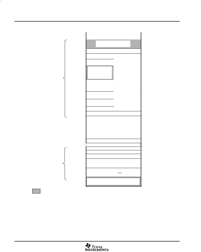
Functional Overview
Low 64K (24x/240x Equivalent Data Space)
High 64K |
(24x/240x Equivalent |
Program Space) |
LEGEND:
Block
Start Address
0x00 0000
0x00 0040
0x00 0400
0x00 0800
0x00 0D00
0x00 0E00
0x00 2000
0x00 6000
0x00 7000
0x00 8000
0x00 9000
0x00 A000
0x3D 7800
0x3D 7C00 0x3D 8000 0x3F 7FF8 0x3F 8000
0x3F A000
0x3F F000
0x3F FFC0
On-Chip Memory
Data Space |
Prog Space |
|
|
M0 Vector − RAM (32 × 32)
(Enabled if VMAP = 0)
M0 SARAM (1K × 16)
M1 SARAM (1K × 16)
Peripheral Frame 0
PIE Vector - RAM
(256 × 16)
Reserved
(Enabled if VMAP = 1, ENPIE = 1)
Reserved
Reserved
Peripheral Frame 1
(Protected)
Reserved
Peripheral Frame 2
(Protected)
L0 SARAM (4K × 16, Secure Block)
L1 SARAM (4K × 16, Secure Block)
Reserved
OTP (or ROM) (1K × 16, Secure Block)
Reserved (1K)
Flash (or ROM) (128K × 16, Secure Block)
128-Bit Password
H0 SARAM (8K × 16)
Reserved
Boot ROM (4K × 16)
(Enabled if MP/MC = 0)
BROM Vector - ROM (32 × 32)
(Enabled if VMAP = 1, MP/MC = 0, ENPIE = 0)
Only one of these vector maps—M0 vector, PIE vector, BROM vector, XINTF vector—should be enabled at a time.
NOTES: A. Memory blocks are not to scale.
B.Reserved locations are reserved for future expansion. Application should not access these areas.
C.Peripheral Frame 0, Peripheral Frame 1, and Peripheral Frame 2 memory maps are restricted to data memory only. User program cannot access these memory maps in program space.
D.“Protected” means the order of Write followed by Read operations is preserved rather than the pipeline order.
E.Certain memory ranges are EALLOW protected against spurious writes after configuration.
Figure 3−3. F2811/C2811 Memory Map
30 |
SPRS174M |
April 2001 − Revised October 2005 |
 Loading...