


Texas Instruments TPS3307-25DR, TPS3307-25DGNR, TPS3307-25DGN, TPS3307-18DR, TPS3307-25D Datasheet
...TPS3307-18, TPS3307-25, TPS3307-33 TRIPLE PROCESSOR SUPERVISORS
SLVS199 ± DECEMBER 1998
DTriple Supervisory Circuits for DSP and Processor-Based Systems
DPower-On Reset Generator with Fixed Delay Time of 200 ms, No External Capacitor Needed
DTemperature-Compensated Voltage Reference
D OR DGN PACKAGE
(TOP VIEW)
SENSE1 |
|
1 |
8 |
|
VDD |
|
|
|
|||||
SENSE2 |
|
|
|
|
|
|
|
2 |
7 |
|
MR |
|
|
|
|
|
||||
SENSE3 |
|
3 |
6 |
|
RESET |
|
|
|
|||||
GND |
|
|
|
|
|
|
|
4 |
5 |
|
RESET |
||
|
|
|
|
|
|
|
|
|
|
|
|
|
|
D D D D D
Maximum Supply Current of 40 μA
Supply Voltage Range . . . 2 V to 6 V Defined RESET Output from VDD ≥ 1.1 V MSOP-8 and SO-8 Packages Temperature Range . . . ± 40°C to 85°C
typical applications
Figure 1 lists some of the typical applications for the TPS3307 family, and a schematic diagram for a processor-based system application. This application uses TI part numbers TPS3307±33 and MSP430C325.
2.5 V 5 V |
3.3 V |
|
VDD |
|
VDD |
|
SENSE 1 |
|
100 nF |
|
|
MSP430C325 |
|
|
|
|
|
|
SENSE 2 |
RESET |
RESET |
470 kΩ |
TPS3307±33 |
|
|
|
SENSE 3 |
|
GND |
|
|
|
|
620 kΩ |
GND |
|
|
|
|
|
|
•Applications using DSPs, Microcontrollers or Microprocessors
•Industrial Equipment
•Programmable Controls
•Automotive Systems
•Portable/Battery Powered Equipment
•Intelligent Instruments
•Wireless Communication Systems
•Notebook/Desktop Computers
Figure 1. Applications Using the TPS3307 Family
description
The TPS3307 family is a series of micropower supply voltage supervisors designed for circuit initialization primarily in DSP and processor-based systems, which require more than one supply voltage.
The product spectrum of the TPS3307-xx is designed for monitoring three independent supply voltages: 3.3 V/1.8 V/adj, 3.3 V/2.5 V/adj or 3.3 V/5 V/adj. The adjustable SENSE input allows the monitoring of any supply voltage >1.25 V.
The various supply voltage supervisors are designed to monitor the nominal supply voltage as shown in the following supply voltage monitoring table.
Please be aware that an important notice concerning availability, standard warranty, and use in critical applications of
Texas Instruments semiconductor products and disclaimers thereto appears at the end of this data sheet.
PRODUCTION DATA information is current as of publication date. Products conform to specifications per the terms of Texas Instruments standard warranty. Production processing does not necessarily include testing of all parameters.
Copyright 1998, Texas Instruments Incorporated
POST OFFICE BOX 655303 •DALLAS, TEXAS 75265 |
1 |
TPS3307-18, TPS3307-25, TPS3307-33
TRIPLE PROCESSOR SUPERVISORS
SLVS199 ± DECEMBER 1998
description (continued)
SUPPLY VOLTAGE MONITORING
DEVICE |
NOMINAL SUPERVISED VOLTAGE |
THRESHOLD VOLTAGE (TYP) |
|||||
|
|
|
|
|
|
||
SENSE1 |
SENSE2 |
SENSE3 |
SENSE1 |
SENSE2 |
SENSE3 |
||
|
|||||||
|
|
|
|
|
|
|
|
TPS3307-18 |
3.3 V |
1.8 V |
User defined |
2.93 V |
1.68 V |
1.25 V² |
|
TPS3307-25 |
3.3 V |
2.5 V |
User defined |
2.93 V |
2.25 V |
1.25 V² |
|
TPS3307-33 |
5 V |
3.3 V |
User defined |
4.55 V |
2.93 V |
1.25 V² |
|
² The actual sense voltage has to be adjusted by an external resistor divider according to the application requirements.
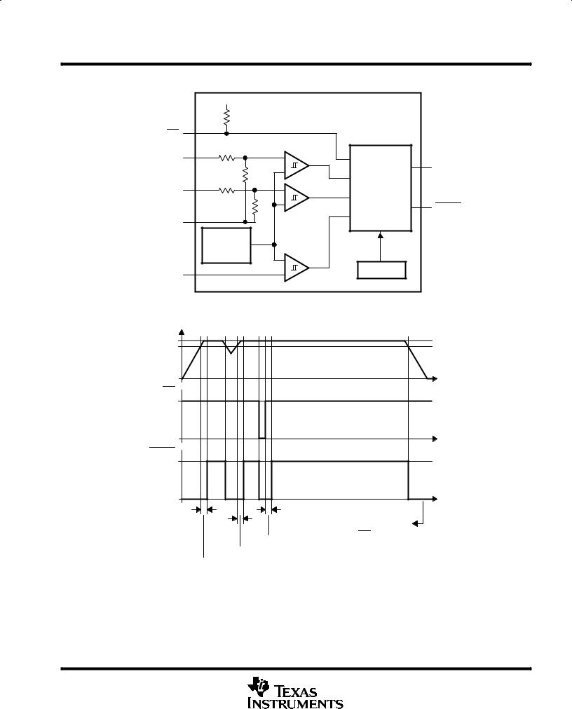
During power-on, RESET is asserted when the supply voltage VDD becomes higher than 1.1 V. Thereafter, the
supply voltage supervisor monitors the SENSEn inputs and keeps RESET active as long as SENSEn remain below the threshold voltage VIT+.
An internal timer delays the return of the RESET output to the inactive state (high) to ensure proper system reset. The delay time, td typ = 200 ms, starts after all SENSEn inputs have risen above the threshold voltage VIT+. When
the voltage at any SENSE input drops below the threshold voltage VIT±, the RESET output becomes active (low) again.
The TPS3307-xx family of devices incorporates a manual reset input, MR. A low level at MR causes RESET to become active. In addition to the active-low RESET output, the TPS3307-xx family includes an active-high RESET output.
The devices are available in either 8-pin MSOP or standard 8-pin SO packages.
The TPS3307-xx devices are characterized for operation over a temperature range of ± 40°C to 85°C.
AVAILABLE OPTIONS
|
PACKAGED DEVICES |
|
|
||
|
|
|
MARKING |
CHIP FORM |
|
TA |
SMALL OUTLINE |
PowerPAD |
|||
μ-SMALL OUTLINE |
DGN PACKAGE |
(Y) |
|||
|
(D) |
||||
|
(DGN) |
|
|
||
|
|
|
|
||
|
|
|
|
|
|
|
TPS3307-18D |
TPS3307-18DGN |
TIAAP |
TPS3307-18Y |
|
±40_C to 85_C |
|
|
|
|
|
TPS3307-25D |
TPS3307-25DGN |
TIAAQ |
TPS3307-25Y |
||
|
|
|
|
|
|
|
TPS3307-33D |
TPS3307-33DGN |
TIAAR |
TPS3307-33Y |
|
|
|
|
|
|
|
FUNCTION/TRUTH TABLES
|
|
|
|
|
|
|
|
|
|
|
MR |
SENSE1>VIT1 |
SENSE2>VIT2 |
SENSE3>VIT3 |
RESET |
RESET |
|||
|
L |
X² |
X² |
X |
|
L |
H |
||
|
H |
0 |
0 |
0 |
|
L |
H |
||
|
H |
0 |
0 |
1 |
|
L |
H |
||
|
H |
0 |
1 |
0 |
|
L |
H |
||
|
H |
0 |
1 |
1 |
|
L |
H |
||
|
H |
1 |
0 |
0 |
|
L |
H |
||
|
H |
1 |
0 |
1 |
|
L |
H |
||
|
H |
1 |
1 |
0 |
|
L |
H |
||
|
H |
1 |
1 |
1 |
|
H |
L |
||
|
|
|
|
|
|
|
|
|
|
² X = Don't care
PowerPAD is a trademark of Texas Instruments Incorporated.
2 |
POST OFFICE BOX 655303 •DALLAS, TEXAS 75265 |
TPS3307-18, TPS3307-25, TPS3307-33
TRIPLE PROCESSOR SUPERVISORS
SLVS199 ± DECEMBER 1998
functional block diagram
VDD |
|
TPS3307 |
|
|
14 kΩ |
|
MR |
|
|
|
R1 |
+ |
SENSE 1 |
|
|
|
R2 |
_ |
|
|
|
|
R3 |
+ |
SENSE 2 |
|
|
|
|
_ |
|
|
R4 |
GND |
|
|
|
Reference |
|
|
Voltage |
|
|
of 1.25 V |
_ |
|
|
|
SENSE 3 |
|
+ |
RESET
RESET
Logic + Timer
RESET
Oscillator |
timing diagram
SENSEn |
V(nom) |
VIT± |
t |
MR  1
1
0 |
t |
RESET  1
1
0 |
|
t |
td |
td |
td |
|
RESET Because of SENSE Below VIT |
|
|
|
 RESET Because of MR
 RESET Because of SENSE Below VIT±
 RESET Because of SENSE Below VIT±
POST OFFICE BOX 655303 •DALLAS, TEXAS 75265 |
3 |

TPS3307-18, TPS3307-25, TPS3307-33
TRIPLE PROCESSOR SUPERVISORS
SLVS199 ± DECEMBER 1998
TPS3307Y chip information
These chips, when properly assembled, display characteristics similar to those of the TPS3307. Thermal compression or ultrasonic bonding may take place on the doped aluminium bonding pads. The chips may be mounted with conductive epoxy or a gold-silicon preform.
(1) |
|
(8) |
(2) |
(7) |
|
|
TPS3307Y |
|
|
|
|
(3) |
(6) |
|
|
|
|
(4) |
(5) |
|
48
CHIP THICKNESS: 10 TYPICAL
BONDING PADS: 4 × 4 MINIMUM
TJ max = 150°C
TOLERANCES ARE ± 10%.
ALL DIMENSIONS ARE IN MILS
56
|
|
|
|
|
|
Terminal Functions |
|
|
|
|
|
|
|
|
TERMINAL |
I/O |
DESCRIPTION |
|||
|
NAME |
NO. |
||||
|
|
|
||||
|
|
|
|
|
|
|
|
GND |
4 |
|
Ground |
||
|
|
|
|
|
|
|
|
|
|
|
7 |
I |
Manual reset |
|
MR |
|
|
|||
|
|
|
|
|
||
|
|
|
|
5 |
O |
Active-low reset output |
|
RESET |
|
||||
|
|
|
|
|
||
|
RESET |
6 |
O |
Active-high reset output |
||
|
|
|
|
|
||
|
SENSE1 |
1 |
I |
Sense voltage input 1 |
||
|
|
|
|
|
||
|
SENSE2 |
2 |
I |
Sense voltage input 2 |
||
|
|
|
|
|
||
|
SENSE3 |
3 |
I |
Sense voltage input 3 |
||
|
|
|
|
|
||
|
VDD |
8 |
|
Supply voltage |
||
4 |
POST OFFICE BOX 655303 •DALLAS, TEXAS 75265 |
 Loading...