


TMS320LC203PZA
Texas Instruments TMS320LC203PZA, TMS320LC203PZ, TMS320C203PZA57, TMS320C203PZA, TMS320C203PZ80 Datasheet
...
D
Based Upon the T320C2xLP Core CPU
D
16-Bit Fixed-Point DSP Architecture
– Six Internal Buses for Increased
Parallelism and Performance
– 32-Bit ALU/Accumulator
– 16 × 16-Bit Single-Cycle Multiplier With a
32-Bit Product
– Block Moves for Data, Program,
I/O Space
– Hardware Repeat Instruction
D
Instruction Cycle Time
’C203 ’LC203 ’C209
50 ns @ 5 V 50 ns @ 3.3 V 50 ns @ 5 V
35 ns @ 5 V 35 ns @ 5 V
25 ns @ 5 V
D
Source Code Compatible With TMS320C25
D
Upwardly Code-Compatible With
TMS320C5x Devices
D
Four External Interrupts
D
Boot-Loader Option (’C203 Only)
D
TMS320C2xx Integrated Memory:
– 544 × 16 Words of On-Chip Dual-Access
Data RAM
– 4K × 16 Words of On-Chip Single-Access
Program/Data RAM (’C209 only)
– 4K × 16 Words of On-Chip Program ROM
(’C209 Only)
D
224K × 16-Bit Total Addressable External
Memory Space
– 64K Program
– 64K Data
– 64K I/O
description
– 32K Global
TMS320C203, TMS320C209, TMS320LC203
DIGITAL SIGNAL PROCESSORS
SPRS025B – JUNE 1995 – REVISED AUGUST 1998
D
TMS320C2xx Peripherals:
– PLL With Various Clock Options
– ×1, ×2, ×4, 2 (’C203)
– ×2, 2 (’C209)
– On-Chip Oscillator
– One Wait State Software-Programmable
to Each Space (’C209 Only)
– 0 – 7 Wait States Software-Programmable
to Each Space (’C203 Only)
– Six General-Purpose I/O Pins
– On-Chip 20-Bit Timer
– Full-Duplex Asynchronous Serial Port
(UART) (’C203 Only)
– One Synchronous Serial Port With
Four-Level-Deep FIFOs (’C203 Only)
D
Supports Hardware Wait States
D
Designed for Low-Power Consumption
– Fully Static CMOS Technology
– Power-Down IDLE Mode
D
1.1 mA/MIPS at 3.3 V
D
’C203 is Pin-Compatible With TMS320F206
Flash DSP
D
Up to 40-MIPS Performance at 5 V (’C203)
D
20-MIPS Performance at 3.3 V
D
HOLD Mode for Multiprocessor
Applications
D
IEEE-1 149.1†-Compatible Scan-Based
Emulation
D
80- and 100-pin Small Thin Quad Flat
Packages (TQFPs), (PN and PZ Suffixes)
The TMS320C2xx generation of digital signal processors (DSPs) combines strong performance and great
flexibility to meet the needs of signal processing and control applications. The T320C2xLP core CPU that is the
basis of all ’C2xx devices has been optimized for high speed, small size, and low-power, making it ideal for
demanding applications in many markets. The CPU has an advanced, modified Harvard architecture with six
internal buses that permits tremendous parallelism and data throughput. The powerful ’C2xx instruction set
makes software development easy . And because the ’C2xx is code-compatible with the TMS320C2x and ’C5x
generations, your code investment is preserved. Around this core, ’C2xx-generation devices feature various
combinations of on-chip memory and peripherals. The serial ports provide easy communication with external
devices such as codecs, A/D converters, and other processors. Other peripherals that facilitate the control of
external devices include general-purpose I/O pins, a 20-bit timer, and a wait-state generator.
Please be aware that an important notice concerning availability, standard warranty, and use in critical applications of
Texas Instruments semiconductor products and disclaimers thereto appears at the end of this data sheet.
†
IEEE Standard 1149.1-1990, IEEE Standard Test-Access Port.
PRODUCTION DATA information is current as of publication date.
Products conform to specifications per the terms of Texas Instruments
standard warranty. Production processing does not necessarily include
testing of all parameters.
POST OFFICE BOX 1443 • HOUSTON, TEXAS 77251–1443
Copyright 1998, Texas Instruments Incorporated
1
TMS320C203, TMS320C209, TMS320LC203
I/O PORTS
SUPPLY
TIME
TYPE WITH
DIGITAL SIGNAL PROCESSORS
SPRS025B – JUNE 1995 – REVISED AUGUST 1998
description (continued)
Because of their strong performance, low cost, and easy-to-use development environment, ’C2xx-generation
DSPs are an ideal choice for applications such as smart phones, digital cameras, modems, remote metering,
and security systems.
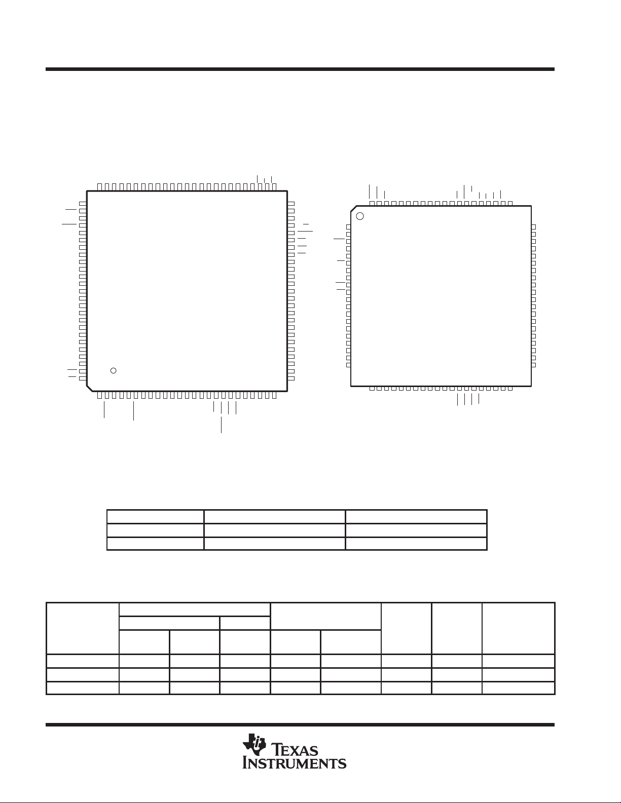
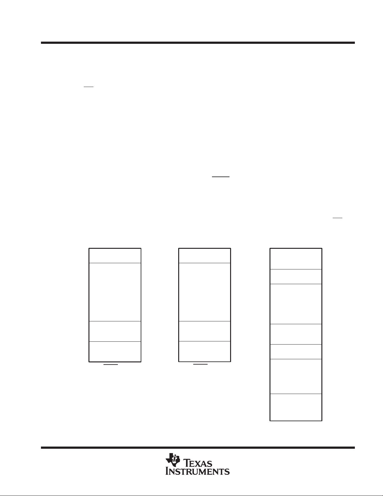
PZ PACKAGE
(TOP VIEW)
PN PACKAGE
(TOP VIEW)
EMU0
EMU1/OFF
TCK
TRST
TDI
TMS
TDO
V
CLKR
FSR
DR
CLKX
V
FSX
DX
V
TOUT
V
RX
IO0
IO1
BIO
RS
A14
A13
A12VA11
DD
DIV1VDIV2
SS
DD
V
HOLDA
SS
A10A9A8VA7VA6A5A4VA3A2A1A0VPSIS
DD
IO2
IO3
V
PLL5V
CLKIN/X2
DD
V
A15
76
77
78
79
80
81
82
83
SS
84
85
86
87
88
SS
89
90
91
DD
92
TX
93
94
SS
95
96
97
XF
98
99
TEST
BOOT
DD
X1
SS
V
CLKOUT1
SS
DD
NMI
V
HOLD /INT1
INT2
INT3
SS
V
SS
D0D1D2
DS
DD
51525354555657585960616263646566676869707172737475
50
V
DD
49
READY
48
V
SS
47
R/W
46
STRB
45
RD
44
WE
43
BR
42
V
SS
41
D15
40
D14
39
D13
38
D12
37
V
SS
36
D11
35
V
DD
34
D10
33
D9
32
D8
31
D7
V
30
SS
D6
29
D5
28
D4
27
D3
26100
25242322212019181716151413121110987654321
SS
V
V
EMU0
EMU1/OFF
TDI
READY
TCK
BIO
MP/MC
D15
V
D14
D13
V
D12
D11
D10
DD
RS
RS
SS
DD
D9
D8
TRST
IACKRDV
77
78
79
80
1
2
3
4
5
6
7
8
9
10
11
12
13
14
15
16
17
18
19
20
24
23
22
21
D7D6D5D4D3SSD1
SS
SS
V
V
XF
CLKOUT1
75
76
26
25
SS
V
TOUT
CLKMOD
72
73
74
29
28
27
D2
V
TDO
71
30
X1
CLKIN/X2
69
70
32
31
D0
TMS
BR
68
33
INT1
STRB
67
34
INT2
R/W
66
35
INT3
PSISDSWEV
63
64
65
38
37
36
NMI
PLL5V
RAMEN
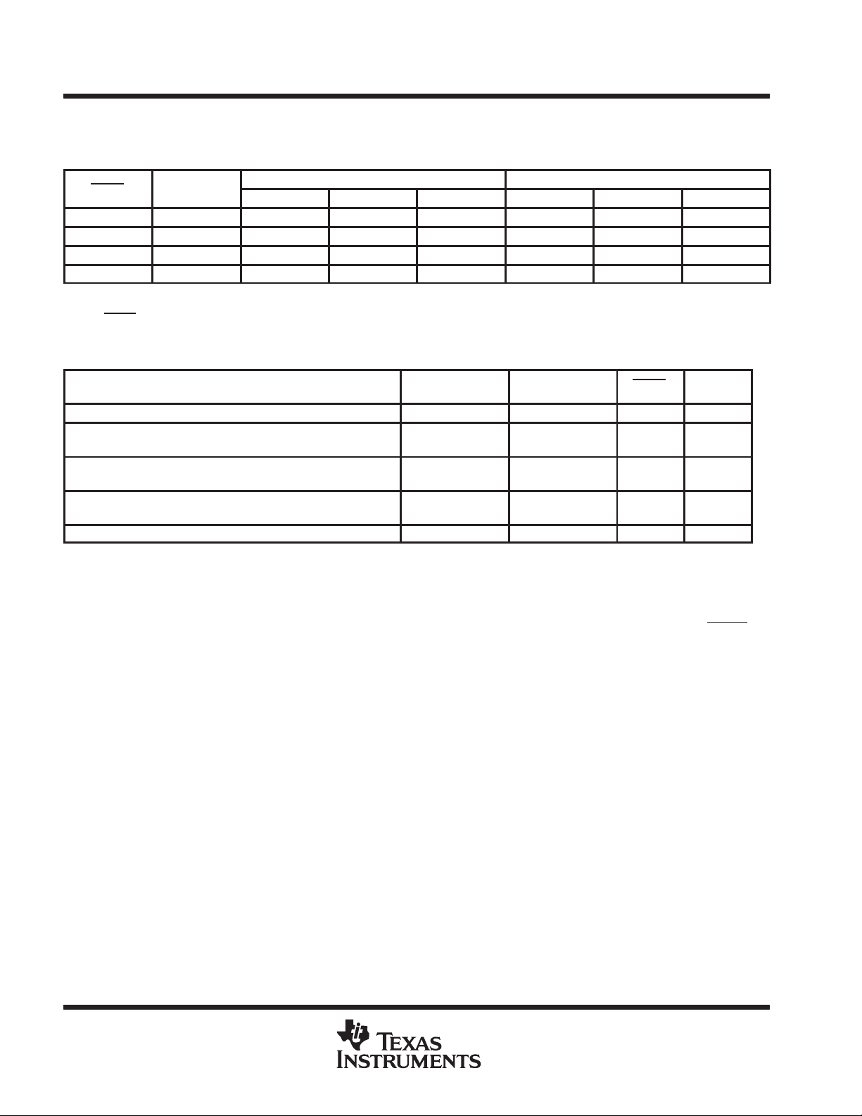
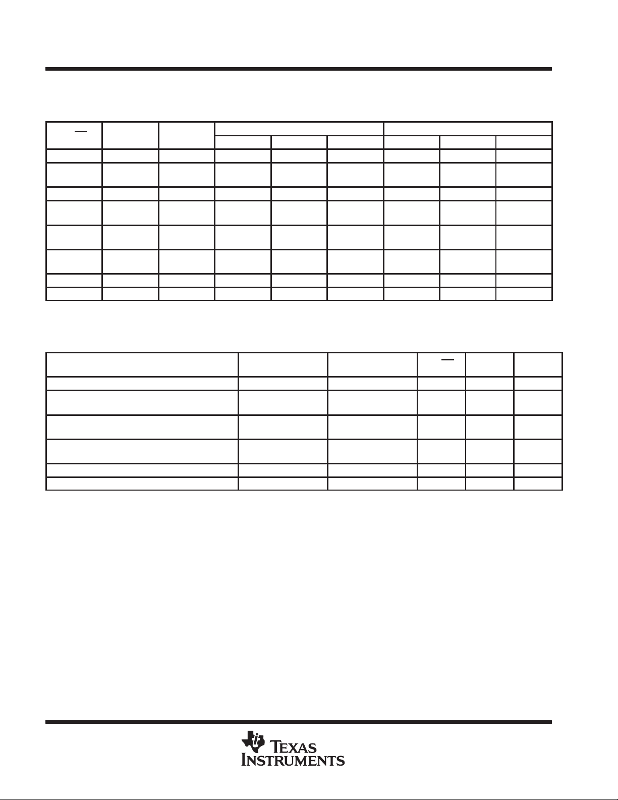
Table 2 provides a comparison of the devices in the ’C2xx generation. It shows the capacity of on-chip RAM
and ROM, the number of serial and parallel I/O ports, the execution time of one machine cycle, and the type
of package with total pin count.
SS
61
62
A15
60
A14
59
A13
58
A12
57
V
56
SS
A11
55
A10
54
A9
53
A8
52
V
51
DD
V
50
DD
A7
49
A6
48
V
47
SS
A5
46
A4
45
A3
44
A2
43
A1
42
V
41
SS
40
39
A0
RES1
Table 1. Low Power Dissipation
†
POWER TMS320C203 TMS320C209
3.3 V 1.1 mA/MIPS N/A
5 V 1.9 mA/MIPS 1.9 mA/MIPS
†
Core power dissipation. For complete details, see
Calculation of TMS320C2xx Power Dissipation
(literature
number SPRA088).
Table 2. Characteristics of the TMS320C2xx Processors
ON-CHIP MEMORY
TMS320C2xx
DEVICES
RAM ROM
DATA
DATA/
PROG
PROG SERIAL PARALLEL
TMS320C203 288 256 – 2 64K 5 50/35/25 100-pin TQFP
TMS320C209 288 4K + 256 4K – 64K 5 50/35 80-pin TQFP
TM320LC203 288 256 – 2 64K 3.3 50 100-pin TQFP
2
POST OFFICE BOX 1443 • HOUSTON, TEXAS 77251–1443
POWER
(V)
CYCLE
(ns)
PACKAGE
PIN COUNT
TYPE
†
DESCRIPTION
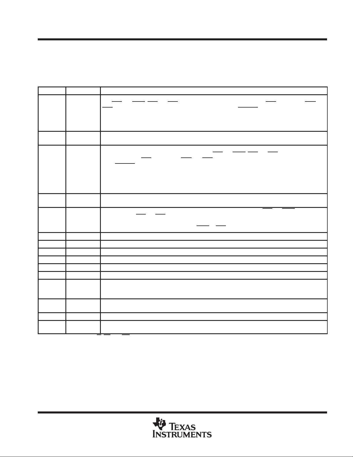
TMS320C203 and TMS320LC203 Terminal Functions
TERMINAL
NAME NO.
DATA AND ADDRESS BUSES
D15
D14
D13
D12
D11
D10
D9
D8
D7
D6
D5
D4
D3
D2
D1
D0
A15
A14
A13
A12
A11
A10
A9
A8
A7
A6
A5
A4
A3
A2
A1
A0
PS 53 O/Z
DS 51 O/Z
IS 52 O/Z
READY 49 I
R/W 47 O/Z
RD 45 O/Z
WE 44 O/Z
†
I = input, O = output, Z = high impedance, PWR = power, GND = ground
41
40
39
38
36
34
33
32
31
29
28
27
26
24
23
22
74
73
72
71
69
68
67
66
64
62
61
60
58
57
56
55
I/O/Z
O/Z
Parallel data bus D15 [most significant bit (MSB)] through D0 [least significant bit (LSB)]. D15–D0 are
multiplexed to transfer data between the TMS320C2xx and external data/program memory or I/O
devices. Placed in the high-impedance state when not outputting (R/W
go into the high-impedance state when OFF
Parallel address bus A15 (MSB) through A0 (LSB). A15–A0 are multiplexed to address external
data/program memory or I/O devices. These signals go into the high-impedance state when OFF
low.
MEMORY CONTROL SIGNALS
Program-select signal. PS is always high unless low-level asserted for communicating to off-chip program
space. PS
Data-select signal. DS is always high unless low-level asserted for communicating to off-chip program
space. DS
I/O space-select signal. IS is always high unless low-level asserted for communicating to I/O ports. IS
goes into the high-impedance state when OFF is active low.
Data-ready input. READY indicates that an external device is prepared for the bus transaction to be
completed. If the external device is not ready (READY low), the TMS320C203 waits one cycle and checks
READY again. If READY is not used, it should be pulled high.
Read/write signal. R/W indicates transfer direction when communicating to an external device. R/W is
normally in read mode (high), unless low level is asserted for performing a write operation. R/W
the high-impedance state when OFF
Read-select indicates an active, external read cycle and can connect directly to the output enable (OE)
of external devices. RD
high-impedance state when OFF
Write enable. The falling edge of WE indicates that the device is driving the external data bus (D15–D0).
Data can be latched by an external device on the rising edge of WE
data, and I/O writes. WE
goes into the high-impedance state when OFF is active low.
goes into the high-impedance state when OFF is active low.
is active on all external program, data, and I/O reads. RD goes into the
goes into the high-impedance state when OFF is active low.
TMS320C203, TMS320C209, TMS320LC203
DIGITAL SIGNAL PROCESSORS
SPRS025B – JUNE 1995 – REVISED AUGUST 1998
high) or RS when asserted. They
is active low.
is active
goes into
is active low.
is active low.
. WE is active on all external program,
POST OFFICE BOX 1443 • HOUSTON, TEXAS 77251–1443
3
TMS320C203, TMS320C209, TMS320LC203
TYPE
†
DESCRIPTION
DIGITAL SIGNAL PROCESSORS
SPRS025B – JUNE 1995 – REVISED AUGUST 1998
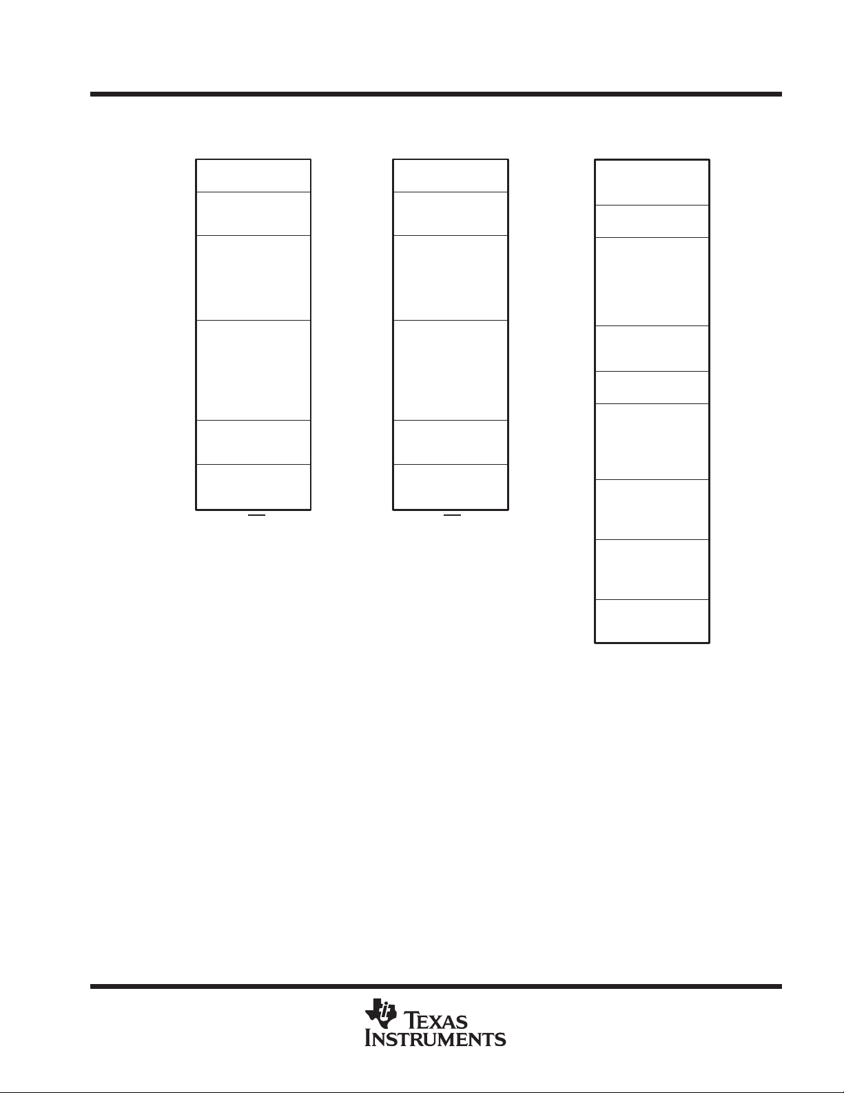
TMS320C203 and TMS320LC203 Terminal Functions (Continued)
TERMINAL
NAME NO.
MEMORY CONTROL SIGNALS (CONTINUED)
STRB 46 O/Z
BR 43 O/Z
HOLDA 6 O/Z
XF 98 O/Z
BIO 99 I
IO0
IO1
IO2
IO3
RS 100 I
TEST 1 I Reserved input pin. TEST is connected to VSS for normal operation.
BOOT 2 I
NMI 17 I
HOLD/INT1 18 I
INT2
INT3
TOUT 92 O
CLKOUT1 15 O/Z
CLKIN/X2
X1
DIV1
DIV2
†
I = input, O = output, Z = high impedance, PWR = power, GND = ground
96
97
19
20
12
13
I/O/Z
8
9
3
5
Strobe signal. STRB is always high unless asserted low to indicate an external bus cycle. STRB goes into the
high-impedance state when OFF
MULTI-PROCESSING SIGNALS
Bus-request signal. BR is asserted when a global data-memory access is initiated. BR goes into the
high-impedance state when OFF
Hold-acknowledge signal. HOLDA indicates to the external circuitry that the processor is in a hold state and
that the address, data, and memory control lines are in the high-impedance state so that they are available to
the external circuitry for access of local memory. HOLDA
active low.
External flag output (latched software-programmable signal). XF is used for signalling other processors in
multiprocessing configurations or as a general-purpose output pin. XF goes into the high-impedance state
when OFF
Branch control input. When polled by the BIOZ instruction, if BIO is low, the TMS320C203 executes a
branch. If BIO
Software-controlled input/output pins by way of the asynchronous serial-port control register (ASPCR). At
reset, IO0–IO3 are configured as inputs. These pins can be used as general-purpose input/output pins or as
handshake control for the UART. IO0–IO3 go into the high-impedance state when OFF
Reset input. RS causes the TMS320C203 to terminate execution and forces the program counter to zero.
When RS
various registers and status bits.
Microprocessor-mode-select pin. When BOOT is high, the device accesses off-chip memory. If BOOT is low ,
the on-chip boot-loader transfers data from external global data space to external RAM program space.
Nonmaskable interrupt. NMI is an external interrupt that cannot be masked by way of the interrupt-mode bit
(INTM) or the interrupt mask register (IMR). When NMI
vector location. If NMI
HOLD and INT1 share the same pin. Both are treated as interrupt signals. If the MODE bit is 0 in the
interrupt-control register (ICR), hold logic can be implemented in combination with the IDLE instruction in
software. At reset, the MODE bit in ICR is zero, enabling the HOLD mode for the pin.
External user interrupts. INT2 and INT3 are prioritized and maskable by the IMR and the INTM. INT2 and INT3
can be polled and reset by way of the interrupt flag register (IFR). If these signals are not used, they should
I
be pulled high.
Timer output. TOUT signals a pulse when the on-chip timer counts down past zero. The pulse is one
CLKOUT1-cycle wide. TOUT goes into the high-impedance state when OFF
Master clock ouput signal. The CLKOUT1 high pulse signifies the logic phase while the low pulse signifies the
latch phase.
Input clock. CLKIN/X2 is the input clock to the device. As CLKIN, the pin operates as the external oscillator
I
clock input, and as X2, the pin operates as the internal oscillator input with X1 being the internal oscillator
O
output.
DIV1 and DIV2 provide clock-mode inputs.
I
DIV1–DIV2 should not be changed unless the RS
is active low.
is not used, it should be pulled high.
INITIALIZATION, INTERRUPTS, AND RESET OPERATIONS
is brought high, execution begins at location 0 of program memory after 16 cycles. RS affects
is not used, it should be pulled high.
OSCILLATOR, PLL, AND TIMER SIGNALS
is active low.
is active low.
goes into the high-impedance state when OFF is
is activated, the processor traps to the appropriate
signal is active.
is active low.
is active low.
4
POST OFFICE BOX 1443 • HOUSTON, TEXAS 77251–1443
TYPE
†
DESCRIPTION
TMS320C203, TMS320C209, TMS320LC203
DIGITAL SIGNAL PROCESSORS
SPRS025B – JUNE 1995 – REVISED AUGUST 1998
TMS320C203 and TMS320LC203 Terminal Functions (Continued)
TERMINAL
NAME NO.
OSCILLATOR, PLL, AND TIMER SIGNALS (CONTINUED)
PLL5V 10 I
CLKX 87 I/O
CLKR 84 I/O
FSR 85 I/O
FSX 89 I/O
DR 86 I Serial-data receive input. Serial data is received in the receive shift register (RSR) through the DR pin.
DX 90 O
TX 93 O Asynchronous transmit pin
RX 95 I Asynchronous receive pin
TRST 79 I
TCK 78 I
TMS 81 I JTAG test-mode select. TMS is clocked into the TAP controller on the rising edge of TCK.
TDI 80 I JTAG test-data input. TDI is clocked into the selected register (instruction or data) on a rising edge of TCK.
TDO 82 O/Z
EMU0 76 I/O/Z
EMU1/OFF 77 I/O/Z
†
I = input, O = output, Z = high impedance, PWR = power, GND = ground
PLL operating at 5 V. When the device is operating at 5 V, PLL5V should be tied high. When the device is
operating at 3.3 V, PLL5V should be tied low.
SERIAL PORT AND UART SIGNALS
Transmit clock. CLKX is a clock signal for clocking data from the transmit shift register (XSR) to the DX
data-transmit pin. The CLKX can be an input if the MCM bit in the synchronous serial-port control register
(SSPCR) is set to 0. CLKX can also be driven by the device at one-half of the CLKOUT1 frequency when
MCM = 1. If the serial port is not being used, CLKX goes into the high-impedance state when OFF
low. Value at reset is as an input.
Receive-clock input. External clock signal for clocking data from the DR (data-receive) pin into the serial-port
receive shift register (RSR). CLKR must be present during serial-port transfers. If the serial port is not being
used, CLKR can be sampled as an input by the IN0 bit of the SSPCR.
Frame synchronization pulse for receive input. The falling edge of the FSR pulse initiates the data-receive
process, beginning the clocking of the RSR. FSR goes into the high-impedance state when OFF
Frame synchronization pulse for transmit input/ouput. The falling edge of the FSX pulse initiates the
data-transmit process, beginning the clocking of the serial-port transmit shift register (XSR). Following reset,
FSX is an input. FSX can be selected by software to be an output when the TXM bit in the SSPCR is set to
1. FSX goes into the high-impedance state when OFF
Serial-port transmit output. Serial data is transmitted from the transmit shift register (XSR) through the DX pin.
DX is in the high-impedance state when OFF
TEST SIGNALS
IEEE Standard 1149.1 (JTAG) test reset. TRST, when active high, gives the scan system control of the
operations of the device. If TRST
and the test signals are ignored.
If the TRST
JTAG test clock. TCK is normally a free-running clock signal with a 50% duty cycle. The changes on the
test-access port (TAP) input signals (TMS and TDI) are clocked into the TAP controller , instruction register , or
selected test-data register on the rising edge of TCK. Changes at the TAP output signal (TDO) occur on the
falling edge of TCK.
JTAG test-data output. The contents of the selected register (instruction or data) are shifted out of TDO on the
falling edge of TCK. TDO is in the high-impedance state except when the scanning of data is in progress.
Emulator pin 0. When TRST is driven low, EMU0 must be high for activation of the OFF condition. When TRST
is driven high, EMU0 is used as an interrupt to or from the emulator system and is defined as an input/output
through the JTAG scan.
Emulator pin 1. Emulator pin 1 disables all outputs. When TRST is driven high, EMU1/OFF is used as an
interrupt to or from the emulator system and is defined as an input/output through the JT AG scan. When TRST
is driven low, this pin is configured as OFF. EMU1/OFF, when active low, puts all output drivers in the
high-impedance state. Note that OFF
multiprocessing applications). Therefore, for the OFF
TRST
EMU0 = 1
EMU/OFF
pin is not driven, an external pulldown resistor must be used.
= 0
= 0
is not connected or driven low, the device operates in its functional mode,
is active low.
is used exclusively for testing and emulation purposes (not for
is active low.
condition, the following apply:
is active
is active low.
POST OFFICE BOX 1443 • HOUSTON, TEXAS 77251–1443
5
TMS320C203, TMS320C209, TMS320LC203
TYPE
†
DESCRIPTION
DIGITAL SIGNAL PROCESSORS
SPRS025B – JUNE 1995 – REVISED AUGUST 1998
TMS320C203 and TMS320LC203 Terminal Functions (Continued)
TERMINAL
NAME NO.
SUPPLY PINS
4
7
11
16
V
DD
V
SS
†
I = input, O = output, Z = high impedance, PWR = power, GND = ground
35
50
63
75
91
14
21
25
30
37
42
48
54
59
65
70
83
88
94
PWR Power
GND Ground
6
POST OFFICE BOX 1443 • HOUSTON, TEXAS 77251–1443
TYPE
†
DESCRIPTION
TMS320C203, TMS320C209, TMS320LC203
DIGITAL SIGNAL PROCESSORS
SPRS025B – JUNE 1995 – REVISED AUGUST 1998
TMS320C209 Terminal Functions
TERMINAL
NAME NO.
ADDRESS AND DATA BUSES
D15
D14
D13
D12
D11
D10
D9
D8
D7
D6
D5
D4
D3
D2
D1
D0
A15
A14
A13
A12
A11
A10
A9
A8
A7
A6
A5
A4
A3
A2
A1
A0
PS 65 O/Z
DS 63 O/Z
‡
IS
READY 7 I
‡
R/W
STRB 67 O/Z
RD 78 O/Z
†
I = input, O = output, Z = high impedance, PWR = power, GND = ground
‡
IS
, R/W, and the data bus are visible at the pins, while accessing internal I/O-mapped registers (for ’C209 devices only).
11
13
14
16
17
18
19
20
23
24
25
26
27
28
30
31
60
59
58
57
55
54
53
52
49
48
46
45
44
43
42
39
64 O/Z
66 O/Z
I/O/Z
O/Z
Parallel data bus D15 (MSB) through D0 (LSB). D15–D0 are multiplexed to transfer data between the
core CPU and external data/program memory or I/O devices. D15–D0 are placed in the high-impedance
state when not outputting or when RS
is active low.
Parallel address bus A15 (MSB) through A0 (LSB). A15–A0 are multiplexed to address external
data/program memory or I/O devices. These signals go into the high-impedance state when OFF
active low.
MEMORY CONTROL SIGNALS
Program-select signal. PS is always high unless low-level asserted for communicating to off-chip
program space. PS
Data-select signal. DS is always high unless low-level asserted for communicating to off-chip program
space. DS
I/O-space-select signal. IS is always high unless low-level asserted for communicating to I/O ports. IS
goes into the high-impedance state when OFF is active low.
Data-ready input. READY indicates that an external device is prepared for the bus transaction to be
completed. If READY is low, the TMS320C209 waits one cycle and checks READY again. If READY is
not used, it should be pulled high.
Read/write signal. R/W indicates transfer direction when communicating to an external device. R/W is
normally in read mode (high), unless low level is asserted for performing a write operation. R/W
into the high-impedance state when OFF
Strobe signal. STRB is always high unless asserted low to indicate an external bus cycle. STRB goes
into the high-impedance state when OFF
Read-select. RD indicates an active, external read cycle and can connect directly to the output enable
(OE
high-impedance state when OFF
goes into the high-impedance state when OFF is active low.
) of external devices. RD is active on all external program, data, and I/O reads. RD goes into the
goes into the high-impedance state when OFF is active low.
is asserted. They also go into the high-impedance state when OFF
is active low.
is active low.
is active low.
is
goes
POST OFFICE BOX 1443 • HOUSTON, TEXAS 77251–1443
7
TMS320C203, TMS320C209, TMS320LC203
TYPE
†
DESCRIPTION
DIGITAL SIGNAL PROCESSORS
SPRS025B – JUNE 1995 – REVISED AUGUST 1998
TMS320C209 Terminal Functions (Continued)
TERMINAL
NAME NO.
MEMORY CONTROL SIGNALS (CONTINUED)
Write enable. The falling edge of WE indicates that the device is driving the external data bus (D15–D0).
WE 62 O/Z
RAMEN 37 I RAM enable. RAMEN enables the 4K × 16 words of on-chip RAM.
BR 68 O/Z
BIO 9 I
XF 75 O/Z
IACK 79 O/Z
INT1
INT2
INT3
NMI 36 I
RS
RS
MP/MC 10 I
CLKOUT1 77 O/Z
CLKMOD 74 I
CLKIN/X2
X1
TOUT 72 O
PLL5V 38 I PLL operating at 5 V. When PLL5V is operating at 5 V, PLL5V should be strapped high.
RES1 40 I Reserved input pin. Do not connect to RES1.
†
I = input, O = output, Z = high impedance, PWR = power, GND = ground
33
34
35
69
70
4
6
O
Data can be latched by an external device on the rising edge of WE
data, and I/O writes. WE
MULTIPROCESSING SIGNALS
Bus-request signal. BR is asserted during access of external global data-memory space. BR can be
used to extend the data memory address space by up to 32K words. BR
state when OFF
Branch control input. BIO is polled by BIOZ instruction. If BIO is low, the TMS320C209 executes a
branch. If BIO
External flag output (latched software-programmable signal). XF is used for signaling other processors
in multiprocessing configurations or as a general-purpose output pin.
Interrupt-acknowledge signal. IACK indicates receipt of an interrupt and that the program counter is
fetching the interrupt vector location designated by A15–A0. IACK
state when OFF
INITIALIZATION, INTERRUPT, AND RESET OPERATIONS
External-user interrupts. INT1–INT3 are prioritized and maskable by the interrupt-mask register and the
I
interrupt-mode bit. If INT1
Nonmaskable interrupt. NMI is an external interrupt that cannot be masked through the INTM or the IMR.
When NMI
be pulled high.
Reset input. RS and RS cause the TMS320C209 to terminate execution and force the program counter
to 0. When RS
I
affects various registers and status bits.
Microprocessor/microcontroller-mode-select pin. If MP/MC is low, the on-chip ROM is mapped into
program space. When MP/MC
Master clock output signal. CLKOUT1 cycles at the machine-cycle rate of the CPU. The internal machine
cycle is bounded by the rising edges of CLKOUT1. CLKOUT1 goes into the high-impedance state when
OFF
is active low.
Clock-input mode. CLKMOD (when high) enables the clock doubler and phase-locked loop (PLL) on the
clock input signal. If the internal oscillator is not used, X1 should be left unconnected.
Input clock. CLKIN/X2 is the input clock to the device. As CLKIN, the pin operates as the external
I
oscillator clock input, and as X2, the pin operates as the internal oscillator input with X1 being the internal
oscillator output.
Timer output. TOUT signals a pulse when the on-chip timer counts down past zero. The pulse is one
CLKOUT1-cycle wide.
is not used, it should be pulled high.
is activated, the processor traps to the appropriate vector location. If NMI is not used, it should
is brought high, execution begins at location 0 of program memory after 16 cycles. RS
OSCILLATOR/TIMER SIGNALS CLKIN1/2
goes into the high-impedance state when OFF is active low.
is active low.
is active low.
–INT3 are not used, they should be pulled high.
is high, the device accesses off-chip memory.
. WE is active on all external program,
goes into the high-impedance
also goes into the high-impedance
8
POST OFFICE BOX 1443 • HOUSTON, TEXAS 77251–1443
TYPE
†
DESCRIPTION
TMS320C203, TMS320C209, TMS320LC203
DIGITAL SIGNAL PROCESSORS
SPRS025B – JUNE 1995 – REVISED AUGUST 1998
TMS320C209 Terminal Functions (Continued)
TERMINAL
NAME NO.
TEST SIGNALS
JTAG test clock. TCK is normally a free-running clock signal with a 50% duty cycle. The changes on
TCK 8 I
TDI 5 I
TDO 71 O/Z
TMS 32 I JTAG test mode-select. TMS is clocked into the TAP controller on the rising edge of TCK.
TRST 80 I
EMU0
EMU1/OFF
V
DD
V
SS
†
I = input, O = output, Z = high impedance, PWR = power, GND = ground
15
50
51
76
12
21
22
29
41
47
56
61
73
2
3
1
I/O/Z
PWR Power
GND Ground
test-access port (TAP) input signals (TMS and TDI) are clocked into the TAP controller, instruction
register, or selected test-data register on the rising edge of TCK. Changes at the T AP output signal (TDO)
occur on the falling edge of TCK.
JTAG test data input. TDI is clocked into the selected register (instruction or data) on a rising edge of
TCK.
JTAG test data output. The contents of the selected register (instruction or data) are shifted out of TDO
on the falling edge of TCK. TDO is in the high-impedance state except when scanning of data is in
progress. TDO goes into the high-impedance state when OFF
JTAG test reset. TRST, when active high, gives the JTAG scan system control of the operations of the
device. If TRST
signals are ignored.
Emulator pin 0. When TRST is driven low, EMU0 must be high for activation of the OFF condition. When
TRST
is driven high, EMU0 is used as an interrupt to or from the emulator system and is defined as an
input/output through the JTAG scan.
Emulator pin 1. EMU1 disables all outputs. When TRST
to or from the emulator system and is defined as input/output by way of JTAG scan. When TRST
low, this pin is configured as OFF
ance state.
is not connected or driven low, the device operates in its functional mode, and the JT AG
. EMU1/OFF , when active low, puts all output drivers in the high-imped-
SUPPLY PINS
is active low.
is driven high, EMU1/OFF is used as an interrupt
is driven
POST OFFICE BOX 1443 • HOUSTON, TEXAS 77251–1443
9

TMS320C203, TMS320C209, TMS320LC203
DIGITAL SIGNAL PROCESSORS
SPRS025B – JUNE 1995 – REVISED AUGUST 1998
functional block diagram of the ’C2xx internal hardware
DIV1
DIV2
IS
DS
PS
R/W
STRB
READY
BR
XF
†
HOLD
†
HOLDA
RS
BOOT/MP/MC
INT[3:1]
3
A15–A0
D15–D0
Timer
TOUT
TX
RX
I/O PINS
DX
CLKX
FSX
DR
FSR
CLKR
†
Not available on all devices (see Table 2).
TCR
PRD
TIM
ASP
ADTR
IOSR
BRD
4
SSP
SSPCR
SDTR
Reserved
I/O-Mapped Registers
†
†
16
Data Bus
Memory Map
GREG (16)
16
16
3
Register
IMR (16)
IFR (16)
NOTES: A. Symbol descriptions appear in Table 3.
B. For clarity, the data and program buses are shown as single buses although they include address and data bits.
Control
MUXMUX
ARP(3)
ARB(3)
3
3
MUX
Data/Prog
SARAM
MUX
16
X1
CLKOUT1
CLKIN/X2
16
RD
WE
NMI
16
16
16
3
†
16
16
MUX
Data/Prog
DARAM
B0 (256x16)
MUX
16
PC
Instruction
ROM/FLASH
Address
16
16
AR0(16)
AR1(16)
AR2(16)
AR3(16)
AR4(16)
AR5(16)
AR6(16)
AR7(16)
ARAU(16)
†
MUX
NPAR
PAR MSTACK
DP(9)
16
MUX
MUX
Data
DARAM
B2 (32x16)
B1 (256x16)
16
Program Bus
9
9
16
MUX
Stack 8 x16
16
7
LSB
from
IR
MUX
ISCALE (0–16)
32
16
16
Program Control
(PCTRL)
16
16
16
16
PSCALE (–6,0,1,4)
CALU(32)
ACCL(16)ACCH(16)C
OSCALE (0–7)
Data Bus
TREG0(16)
Multiplier
PREG(32)
32
MUX
32
32
16
3232
32
MUX
Data Bus
1616
16
Program Bus
Program Bus
10
POST OFFICE BOX 1443 • HOUSTON, TEXAS 77251–1443
TMS320C203, TMS320C209, TMS320LC203
DIGITAL SIGNAL PROCESSORS
SPRS025B – JUNE 1995 – REVISED AUGUST 1998
Table 3. Legend for the ’C2xx Internal Hardware Functional Block Diagram
SYMBOL NAME DESCRIPTION
ACC Accumulator
ARAU
AUX
REGS
BR Bus Register Signal
C Carry
CALU
CNF
GREG
IMR
IFR
INTM Interrupt-Mode Bit
INT# Interrupt Traps A total of 32 interrupts by way of hardware and/or software are available.
ISCALE
MPY Multiplier
MSTACK Micro Stack
MUX Multiplexer Multiplexes buses to a common input
NPAR
OSCALE
PAR Program Address
PC Program Counter
PCTRL Program Controller PCTRL decodes instruction, manages the pipeline, stores status, and decodes conditional operations.
PM
PRDB
Auxiliary Register
Arithmetic Unit
Auxiliary Registers
0–7
Central Arithmetic
Logic Unit
On-Chip RAM
Configuration
Control Bit
Global Memory
Allocation Register
Interrupt Mask
Register
Interrupt Flag
Register
Input Data-Scaling
Shifter
Next Program
Address
Output Data-Scaling
Shifter
Product Shift-Mode
Register Bits
Program-Read Data
Bus
32-bit register that stores the results and provides input for subsequent CALU operations. Also includes
shift and rotate capabilities
An unsigned, 16-bit arithmetic unit used to calculate indirect addresses using the auxiliary registers as
inputs and outputs
These 16-bit registers are used as pointers to anywhere within the data space address range. They are
operated upon by the ARAU and are selected by the auxiliary register pointer (ARP). AR0 can also be used
as an index value for AR updates of more than one and as a compare value to AR.
BR is asserted during access of the external global data memory space. READY is asserted to the device
when the global data memory is available for the bus transaction. BR
memory address space by up to 32K words.
Register carry output from CALU. C is fed back into the CALU for extended arithmetic operation. The C bit
resides in status register 1 (ST1), and can be tested in conditional instructions. C is also used in accumulator
shifts and rotates.
32-bit-wide main arithmetic logic unit for the TMS320C2xx core. The CALU executes 32-bit operations in
a single machine cycle. CALU operates on data coming from ISCALE or PSCALE with data from ACC, and
provides status results to PCTRL.
If set to 0, the reconfigurable data dual-access RAM (DARAM) blocks are mapped to data space; otherwise,
they are mapped to program space.
GREG specifies the size of the global data memory space.
IMR individually masks or enables the seven interrupts.
The 7-bit IFR indicates that the TMS320C2xx has latched an interrupt from one of the seven maskable
interrupts.
When INTM is set to 0, all unmasked interrupts are enabled. When INTM is set to 1, all maskable interrupts
are disabled.
16 to 32-bit barrel left-shifter. ISCALE shifts incoming 16-bit data 0 to16 positions left, relative to the 32-bit
output within the fetch cycle; therefore, no cycle overhead is required for input scaling operations.
16 × 16-bit multiplier to a 32-bit product. MPY executes multiplication in a single cycle. MPY operates either
signed or unsigned 2s-complement arithmetic multiply.
MSTACK provides temporary storage for the address of the next instruction to be fetched when program
address-generation logic is used to generate sequential addresses in data space.
NPAR holds the program address to be driven out on the PAB on the next cycle.
16-bit to 32-bit barrel left shifter. OSCALE shifts the 32-bit accumulator output 0 to 7 bits left for quantization
management and outputs either the 16-bit high- or low-half of the shifted 32-bit data to DWEB.
PAR holds the address currently being driven on P AB for as many cycles as it takes to complete all memory
operations scheduled for the current machine cycle.
PC increments the value from NPAR to provide sequential addresses for instruction-fetching and sequential
data-transfer operations.
These two bits identify which of the four product-shift modes (–6, 0, 1, 4) are used by PSCALE. PM resides
in ST1. See Table 7.
16-bit bus for program space read data. PRDB is driven by the memories or the logic interface.
can be used to extend the data
POST OFFICE BOX 1443 • HOUSTON, TEXAS 77251–1443
11
TMS320C203, TMS320C209, TMS320LC203
DIGITAL SIGNAL PROCESSORS
SPRS025B – JUNE 1995 – REVISED AUGUST 1998
Table 3. Legend for the ’C2xx Internal Hardware Functional Block Diagram (Continued)
SYMBOL NAME DESCRIPTION
PREG Product Register 32-bit register holds results of 16 × 16 multiply.
0-, 1- or 4-bit left shift, or 6-bit right shift of multiplier product. The left-shift options are used to manage the
PSCALE
TREG
SSPCR
SDTR
TCR
PRD
TIM
UART
ASPCR
ADTR
IOSR
BRD Baud-Rate Divisor Used to set the baud rate of the UART
ST0
ST1
STACK Stack
Product-Scaling
Shifter
Temporary
Register
Synchronous
Serial-Port Control
Register
Synchronous
Serial-Port
Transmit and
Receive Register
Timer-Control
Register
Timer-Period
Register
Timer-Counter
Register
Universal
Asynchronous
Receive/Transmit
Asynchronous
Serial-Port Control
Register
Asynchronous
Data Register
I/O Status
Register
Status Register
additional sign bits resulting from the 2s-complement multiply. The right-shift option is used to scale down
the number to manage overflow of product accumulation in the CALU. PSCALE resides in the path from the
32-bit product shifter and from either the CALU or the Data-Write Address Bus (DWEB), and requires no
cycle overhead.
16-bit register holds one of the operands for the multiply operations. TREG holds the dynamic shift count
for the LACT, ADDT, and SUBT instructions. TREG holds the dynamic bit position for the BITT instruction.
SSPCR is the control register for selecting the serial port’s mode of operation.
SDTR is the data-transmit and data-receive register.
TCR contains the control bits that define the divide-down ratio, start/stop the timer, and reload the period.
Also contained in TCR is the current count in the prescaler. Reset initializes the timer-divide-down ratio
to 0 and starts the timer.
PRD contains the 16-bit period that is loaded into the timer counter when the counter borrows or when the
reload bit is activated. Reset initializes the PRD to 0xFFFF.
TIM contains the current 16-bit count of the timer. Reset initializes the TIM to 0xFFFF.
UART is the asynchronous serial port.
ASPCR controls the asynchronous serial-port operation.
Asynchronous data-transmit and data-receive register
IOSR detects current levels (and changes with inputs) on pins IO0–IO3 and the status of UART.
ST0 and ST1 contain the status of various conditions and modes. These registers can be stored in and
loaded from data memory , thereby allowing the status of the machine to be saved and restored.
STACK is a block of memory used for storing return addresses for subroutines and interrupt-service
routines, or for storing data. The ’C2xx stack is 16-bit wide and eight-level deep.
12
POST OFFICE BOX 1443 • HOUSTON, TEXAS 77251–1443
TMS320C203, TMS320C209, TMS320LC203
DIGITAL SIGNAL PROCESSORS
SPRS025B – JUNE 1995 – REVISED AUGUST 1998
architectural overview
The ’C2xx advanced Harvard-type architecture maximizes the processing power by maintaining two separate
memory bus structures—program and data—for full-speed execution. This multiple bus structure allows both
data and instructions to be read simultaneously . Instructions to be read support data transfers between the two
spaces. This architecture permits coefficients that are stored in program memory to be read in RAM, thereby,
eliminating the need for a separate coefficient ROM. This, coupled with a four-deep pipeline, allows the
TMS320C2xx to execute most instructions in a single cycle.
status and control registers
Two status registers, ST0 and ST1, contain the status of various conditions and modes. These registers can
be stored in data memory and loaded from data memory , thereby, allowing the status of the machine to be saved
and restored for subroutines.
The load-status-register instruction (LST) is used to write to ST0 and ST1. The store-status-register instruction
(SST) is used to read from ST0 and ST1, except for the INTM bit, which is not affected by the LST instruction.
The individual bits of these registers can be set or cleared when using the SETC and CLRC instructions. T able 4
and T able 5 show the organization of status registers ST0 and ST1, indicating all status bits contained in each.
Several bits in the status registers are reserved and read as logic 1s. Refer to T able 6 for the status register field
definitions.
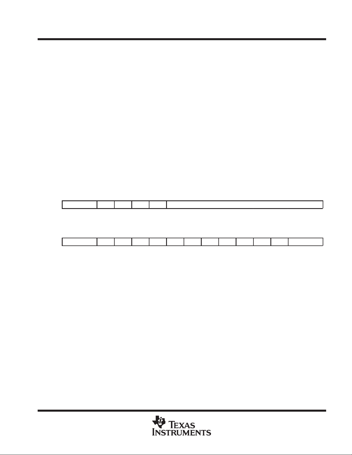
Table 4. Status and Control Register Zero
15 131211109876543210
ST0
ARP
OV OVM 1 INTM DP
Table 5. Status and Control Register One
15 131211109876543210
ST1
ARB
CNF TC SXM C 1 1 1 1 XF 1 1 PM
POST OFFICE BOX 1443 • HOUSTON, TEXAS 77251–1443
13
TMS320C203, TMS320C209, TMS320LC203
DIGITAL SIGNAL PROCESSORS
SPRS025B – JUNE 1995 – REVISED AUGUST 1998
status and control registers (continued)
Table 6. Status Register Field Definitions
FIELD FUNCTION
ARB
ARP
C
CNF
DP
INTM
OV
OVM
PM
SXM
TC
XF
†
See Table 3 for definitions of acronyms and Table 20 for descriptions of opcode instructions.
Auxiliary register pointer buffer . Whenever the ARP is loaded, the old ARP value is copied to the ARB, except during an LST
instruction. When the ARB is loaded by way of an LST #1 instruction, the same value is also copied to the ARP.
Auxiliary register pointer. ARP selects the AR to be used in indirect addressing. When the ARP is loaded, the old ARP value
is copied to the ARB register. ARP can be modified by memory-reference instructions when using indirect addressing, and by
the LARP, MAR, and LST instructions. The ARP is also loaded with the same value as ARB when an LST #1 instruction is
executed.
Carry bit. C is set to 1 if the result of an addition generates a carry; it is reset to 0 if the result of a subtraction generates a borrow.
Otherwise, C is reset after an addition or set after a subtraction, except when the instruction is ADD or SUB with a 16-bit shift.
In these cases, the ADD can only set and the SUB can only reset the carry bit, but cannot affect it otherwise. The single-bit
shift and rotate instructions also affect C, as well as the SETC, CLRC, and LST #1 instructions. Branch instructions have been
provided to branch on the status of C. C is set to 1 on a reset.
On-chip RAM configuration control bit. If CNF is set to 0, the reconfigurable data DARAM blocks are mapped to data space;
otherwise, they are mapped to program space. The CNF can be modified by the SETC CNF, CLRC CNF, and LST #1
instructions. RS
Data-memory page pointer. The 9-bit DP register is concatenated with the seven LSBs of an instruction word to form a direct
memory address of 16 bits. DP can be modified by the LST and LDP instructions.
Interrupt-mode bit. When INTM is set to 0, all unmasked interrupts are enabled. When INTM is set to 1, all maskable interrupts
are disabled. INTM is set and reset by the SETC INTM and CLRC INTM instructions. RS
no effect on the unmaskable RS
by reset. It is also set to 1 when a maskable interrupt trap is taken.
Overflow-flag bit. As a latched overflow signal, OV is set to 1 when overflow occurs in the ALU. Once an overflow occurs, the
OV remains set until a reset, BCND/D on OV/NOV, or LST instruction clears OV.
Overflow-mode bit. When OVM is set to 0, overflowed results overflow normally in the accumulator. When OVM is set to 1, the
accumulator is set to either its most positive or negative value upon encountering an overflow. The SETC and CLRC
instructions set and reset this bit, respectively. LST can also be used to modify the OVM.
Product-shift-mode bits. If these two bits are 00, the multiplier’s 32-bit product is loaded into the ALU with no shift. If PM = 01,
the product register (PREG) output is left-shifted one place and loaded into the ALU, with the LSB zero-filled. If PM = 10, the
PREG output is left-shifted by 4 bits and loaded into the ALU, with the LSBs zero-filled. PM = 11 produces a right shift of 6 bits,
sign-extended. Note that the PREG contents remain unchanged. The shift takes place when transferring the contents of the
PREG to the ALU. PM is loaded by the SPM and LST #1 instructions. PM is cleared by RS
Sign-extension mode bit. SXM = 1 produces sign-extension on data as it is passed into the accumulator through the scaling
shifter. SXM = 0 suppresses sign-extension. SXM does not af fect the definitions of certain instructions; for example, the ADDS
instruction suppresses sign-extension regardless of SXM. SXM is set by the SETC SXM instruction, reset by the CLRC SXM
instruction, and can be loaded by the LST #1 instruction. SXM is set to 1 by reset.
T est/control flag bit. TC is affected by the BIT, BITT , CMPR, LST #1, and NORM instructions. TC is set to a 1 if a bit tested by
BIT or BITT is a 1, if a compare condition tested by CMPR exists between AR (ARP) and AR0, or if the exclusive-OR function
of the two MSBs of the accumulator is true when tested by a NORM instruction. The conditional branch, call, and return
instructions can execute based on the condition of TC.
XF pin status bit. XF indicates the state of the XF pin, a general-purpose output pin. XF is set by the SETC XF and reset by
the CLRC XF instructions. XF is set to 1 by reset.
sets the CNF to 0.
and NMI interrupts. Note that INTM is unaffected by the LST instruction. This bit is set to 1
†
and IACK also set INTM. INTM has
.
central processing unit
The TMS320C2xx central processing unit (CPU) contains a 16-bit scaling shifter, a 16 × 16-bit parallel multiplier ,
a 32-bit central arithmetic logic unit (CALU), a 32-bit accumulator, and additional shifters at the outputs of both
the accumulator and the multiplier. This section describes the CPU components and their functions. The
functional block diagram shows the components of the CPU.
14
POST OFFICE BOX 1443 • HOUSTON, TEXAS 77251–1443
TMS320C203, TMS320C209, TMS320LC203
DIGITAL SIGNAL PROCESSORS
SPRS025B – JUNE 1995 – REVISED AUGUST 1998
input scaling shifter
The TMS320C2xx provides a scaling shifter with a 16-bit input connected to the data bus and a 32-bit output
connected to the CALU. This shifter operates as part of the path of data coming from program or data space
to the CALU and requires no cycle overhead. It is used to align the 16-bit data coming from memory to the 32-bit
CALU. This is necessary for scaling arithmetic as well as aligning masks for logical operations.
The scaling shifter produces a left shift of 0 to 16 on the input data. The LSBs of the output are filled with zeros;
the MSBs can be either filled with zeros or sign-extended, depending upon the value of the SXM bit
(sign-extension mode) of status register ST1. The shift count is specified by a constant embedded in the
instruction word or by a value in the temporary register (TREG). The shift count in the instruction allows for
specific scaling or alignment operations specific to that point in the code. The TREG base shift allows the scaling
factor to be adaptable to the system’s performance.
multiplier
The TMS320C2xx uses a 16 × 16-bit hardware multiplier that is capable of computing a signed or an unsigned
32-bit product in a single machine cycle. All multiply instructions, except the MPYU (multiply unsigned)
instruction, perform a signed multiply operation. That is, two numbers being multiplied are treated as
2s-complement numbers, and the result is a 32-bit 2s-complement number. There are two registers associated
with the multiplier: a 16-bit temporary register (TREG) that holds one of the operands for the multiplier, and a
32-bit product register (PREG) that holds the product.
Four product-shift modes (PM) are available at the PREG’s output (PSCALE). These shift modes are useful for
performing multiply/accumulate operations, performing fractional arithmetic, or justifying fractional products.
The PM field of status register ST1 specifies the PM shift mode, as shown in Table 7.
Table 7. PSCALE Product-Shift Modes
PM SHIFT DESCRIPTION
00 no shift Product feed to CALU or data bus with no shift
01 left 1 Removes the extra sign bit generated in a 2s-complement multiply to produce a Q31 product
10 left 4 Removes the extra four sign bits generated in a 16 × 13 2s-complement multiply to a produce a Q31
11 right 6 Scales the product to allow up to 128 product accumulations without the possibility of accumulator overflow
product when using the multiply by a 13-bit constant
The product can be shifted one bit to compensate for the extra sign bit gained in multiplying two 16-bit
2s-complement numbers (MPY). A 4-bit shift is used in conjunction with the MPY instruction with a short
immediate value (13 bits or less) to eliminate the four extra sign bits gained in multiplying a 16-bit number by
a 13-bit number. Finally, the output of PREG can be right-shifted 6 bits to enable the execution of up to
128 consecutive multiply/accumulates without the possibility of overflow.
The L T (load TREG) instruction normally loads TREG to provide one operand (from the data bus), and the MPY
(multiply) instruction provides the section operand (also from the data bus). A multiplication can also be
performed with a 13-bit immediate operand when using the MPY instruction. A product is then obtained every
two cycles. When the code is executing multiple multiplies and product sums, the CPU supports the pipelining
of the TREG load operations with CALU operations using the previous product. These pipeline operations that
run in parallel with loading the TREG include: load ACC with PREG (L TP); add PREG to ACC (L TA); add PREG
to ACC and shift TREG input data (DMOV) to next address in data memory (L TD); and subtract PREG from ACC
(L TS).
POST OFFICE BOX 1443 • HOUSTON, TEXAS 77251–1443
15

TMS320C203, TMS320C209, TMS320LC203
DIGITAL SIGNAL PROCESSORS
SPRS025B – JUNE 1995 – REVISED AUGUST 1998
multiplier (continued)
Two multiply/accumulate instructions (MAC and MACD) fully utilize the computational bandwidth of the
multiplier, allowing both operands to be processed simultaneously. The data for these operations can be
transferred to the multiplier each cycle by way of the program and data buses. This facilitates single-cycle
multiply/accumulates when used with the repeat (RPT) instruction. In these instructions, the coefficient
addresses are generated by program address generation (PAGEN), while the data addresses are generated
by data-address generation (DAGEN). This allows the repeated instruction to sequentially access the values
from the coefficient table and step through the data in any of the indirect addressing modes.
The MACD instruction, when repeated, supports filter constructs (weighted running averages) so that as the
sum-of-products is executed, the sample data is shifted in memory to make room for the next sample and to
throw away the oldest sample.
The MPYU instruction performs an unsigned multiplication, which greatly facilitates extended-precision
arithmetic operations. The unsigned contents of TREG are multiplied by the unsigned contents of the addressed
data memory location, with the result placed in PREG. This allows the operands of greater than 16 bits to be
broken down into 16-bit words and processed separately to generate products of greater than 32 bits. The
SQRA (square/add) and SQRS (square/subtract) instructions pass the same value to both inputs of the
multiplier for squaring a data-memory value.
After the multiplication of two 16-bit numbers, the 32-bit product is loaded into the 32-bit product register
(PREG). The product from PREG can be transferred to the CALU or to data memory by way of the SPH (store
product-high register) and the SPL (store product-low register) instructions. Note: the transfer of PREG to either
the CALU or data memory passes through the product-scaling shifter (PSCALE) and is therefore affected by
the product-shift mode defined by PM bits in the ST1 register. This is important when saving PREG in an
interrupt-service-routine-context save as the PSCALE shift effects cannot be modeled in the restore operation.
PREG can be cleared by executing the MPY #0 instruction. The product register can be restored by loading the
saved low half into TREG and executing the MPY #1 instruction. The high half is then loaded using the LPH
instruction.
central arithmetic logic unit
The TMS320C2xx central arithmetic logic unit (CALU) implements a wide range of arithmetic and logical
functions, the majority of which execute in a single clock cycle. This arithmetic logic unit (ALU) is referred to as
“central” to differentiate it from a second ALU used for indirect-address-generation (called the ARAU). Once an
operation is performed in the CALU, the result is transferred to the accumulator (ACC), where additional
operations, such as shifting, can occur. Data that is input to the CALU can be scaled by the input data-scaling
shifter (ISCALE) when coming from one of the data buses (DRDB or PRDB) or scaled by PSCALE when coming
from the multiplier.
The CALU is a general-purpose arithmetic/logic unit that operates on 16-bit words taken from data memory or
derived from immediate instructions. In addition to the usual arithmetic instructions, the CALU can perform
Boolean operations, facilitating the bit manipulation ability required for a high-speed controller. One input to the
CALU is always provided from the accumulator, and the other input can be provided from the product register
(PREG) of the multiplier or the output of the scaling shifter (that has been read from data memory or from the
ACC). After the CALU has performed the arithmetic or logical operation, the result is stored in the accumulator.
The TMS320C2xx supports floating-point operations for applications requiring a large dynamic range. The
NORM (normalization) instruction is used to normalize fixed-point numbers contained in the accumulator by
performing left shifts. The four bits of the TREG define a variable shift through the scaling shifter for the
LACT/ADDT/SUBT (load/add to/subtract from accumulator with shift specified by TREG) instructions. These
instructions are useful in floating-point arithmetic where a number needs to be denormalized—that is,
floating-point to fixed-point conversion. They are also useful in the execution of an automatic gain control (AGC)
going into a filter. The BITT (bit-test) instruction provides testing of a single bit of a word in data memory based
on the value contained in the four LSBs of TREG.
16
POST OFFICE BOX 1443 • HOUSTON, TEXAS 77251–1443

TMS320C203, TMS320C209, TMS320LC203
DIGITAL SIGNAL PROCESSORS
SPRS025B – JUNE 1995 – REVISED AUGUST 1998
central arithmetic logic unit (continued)
The CALU overflow-saturation mode can be enabled/disabled by setting/resetting the overflow mode (OVM)
bit of ST0. When the CALU is in the overflow-saturation mode and an overflow occurs, the overflow flag is set
and the accumulator is loaded with either the most positive or the most negative value representable in the
accumulator, depending upon the direction of the overflow. The value of the accumulator upon saturation is
07FFFFFFFh (positive) or 080000000h (negative). If the OVM status register bit is reset and an overflow occurs,
the overflowed results are loaded into the accumulator with modification. (Note that logical operations cannot
result in overflow.)
The CALU can execute a variety of branch instructions that depend on the status of the CALU and the
accumulator. These instructions can be executed conditionally, based on any meaningful combination of these
status bits. For overflow management, these conditions include the OV (branch on overflow) and EQ (branch
on accumulator equal to zero). In addition, the BACC (branch to address in accumulator) instruction provides
the ability to branch to an address specified by the accumulator (computed goto). Bit-test instructions (BIT and
BITT), which do not affect the accumulator, allow the testing of a specified bit of a word in data memory.
The CALU also has a carry bit that is set or reset depending on various operations within the device. The carry
bit allows more efficient computation of extended-precision products and additions or subtractions. It is also
useful in overflow management. The carry bit is affected by most arithmetic instructions as well as the single-bit
shift and rotate instructions. It is not affected by accumulator loads, logical operations, or other such
non-arithmetic or control instructions.
D
Additions to and subtractions from the accumulator:
C = 0: When the result of a subtraction generates a borrow.
When the result of an addition does not generate a carry . (Exception: When the ADD instruction is
used with a shift of 16 and no carry is generated, the ADD instruction has no effect on C.)
C = 1: When the result of an addition generates a carry.
When the result of a subtraction does not generate a borrow. (Exception: When the SUB instruction
is used with a shift of 16 and no borrow is generated, the SUB instruction has no effect on C.)
D
Single-bit shifts and rotations of the accumulator value. During a left shift or rotation, the most significant
bit of the accumulator is passed to C; during a right shift or rotation, the least significant bit is passed to C.
Note: the carry bit is set to “1” on a hardware reset.
The ADDC (add to accumulator with carry) and SUBB (subtract from accumulator with borrow) instructions
provide the use of the previous value of carry in their addition/subtraction operation.
The one exception to the operation of the carry bit is in the use of ADD with a shift count of 16 (add to high
accumulator) and SUB with a shift count of 16 (subtract from high accumulator) instructions. This case of the
ADD instruction can set the carry bit only if a carry is generated, and this case of the SUB instruction can reset
the carry bit only if a borrow is generated; otherwise, neither instruction affects it.
Two conditional operands, C and NC, are provided for branching, calling, returning, and conditionally executing
based upon the status of the carry bit. The SETC, CLRC, and LST #1 instructions also can be used to load the
carry bit. The carry bit is set to one on a hardware reset.
accumulator
The 32-bit accumulator is the registered output of the CALU. It can be split into two 16-bit segments for storage
in data memory. Shifters at the output of the accumulator provide a left shift of 0 to 7 places. This shift is
performed while the data is being transferred to the data bus for storage. The contents of the accumulator
remain unchanged. When the post-scaling shifter is used on the high word of the accumulator (bits 16–31), the
MSBs are lost and the LSBs are filled with bits shifted in from the low word (bits 0–15). When the post-scaling
shifter is used on the low word, the LSBs are zero-filled.
POST OFFICE BOX 1443 • HOUSTON, TEXAS 77251–1443
17

TMS320C203, TMS320C209, TMS320LC203
DIGITAL SIGNAL PROCESSORS
SPRS025B – JUNE 1995 – REVISED AUGUST 1998
accumulator (continued)
The SFL and SFR (in-place one-bit shift to the left/right) instructions and the ROL and ROR (rotate to the
left/right) instructions implement shifting or rotating of the accumulator contents through the carry bit. The SXM
status register bit affects the definition of the SFR (shift accumulator right) instruction. When SXM = 1, SFR
performs an arithmetic right shift, maintaining the sign of the accumulator data. When SXM = 0, SFR performs
a logical shift, shifting out the LSBs and shifting in a zero for the MSB. The SFL (shift accumulator left) instruction
is not affected by the SXM bit and behaves the same in both cases, shifting out the MSB and shifting in a zero.
RPT (repeat) instructions can be used with the shift and rotate instructions for multiple-bit shifts.
auxiliary registers and auxiliary-register arithmetic unit (ARAU)
The ’C2xx provides a register file containing eight auxiliary registers (AR0–AR7). The auxiliary registers are
used for indirect addressing of the data memory or for temporary data storage. Indirect auxiliary-register
addressing allows placement of the data memory address of an instruction operand into one of the auxiliary
registers. These registers are referenced with a 3-bit auxiliary register pointer (ARP) that is loaded with a value
from 0 through 7, designated AR0 through AR7, respectively . The auxiliary registers and the ARP can be loaded
from data memory, the ACC, the product register, or by an immediate operand defined in the instruction. The
contents of these registers can also be stored in data memory or used as inputs to the CALU.
The auxiliary register file is connected to the ARAU. The ARAU can autoindex the current auxiliary register while
the data memory location is being addressed. Indexing either by ±1 or by the contents of AR0 can be performed.
As a result, accessing tables of information does not require the CALU for address manipulation; therefore, the
CALU is free for other operations in parallel.
memory
The ’C2xx implements three separate address spaces for program memory , data memory, and I/O. Each space
accommodates a total of 64K 16-bit words. Within the 64K words of data space, the 256 to 32K words at the
top of the address range can be defined to be external global memory in increments of powers of two, as
specified by the contents of the global memory allocation register. Access to global memory is arbitrated using
the global memory bus request (BR
On the ’C2xx, the first 96 (0–5Fh) data memory locations are allocated for memory-mapped registers or are
reserved. This memory-mapped register space contains various control and status registers including those for
the CPU.
When using on-chip RAM, or high-speed external memory , the ’C2xx runs at full speed with no wait states. The
ability of the DARAM to allow two accesses to be performed in one cycle, coupled with the parallel nature of
the ’C2xx architecture, enables the device to perform three concurrent memory accesses in any given machine
cycle. Externally , the READY line can be used to interface the ’C2xx to slower, less expensive external memory .
Downloading programs from slow off-chip memory to on-chip RAM can speed processing while cutting system
costs.
The ’C2xx DARAM allows writes to and reads from the RAM in the same cycle without the address restrictions
of the SARAM. The DARAM is configured in three blocks: block 0 (B0), block 1 (B1), and block 2 (B2).
Block 1 consists of 256 words in data memory and block 2 consists of 32 words in data memory. Block 0 is a
256-word block that can be configured as data or program memory . The SETC CNF (configure B0 as program
memory) and CLRC CNF (configure B0 as data memory) instructions allow dynamic configuration of the
memory maps through software. When using Block 0 as program memory , instructions can be downloaded from
external program memory into on-chip RAM and then executed.
) signal.
18
POST OFFICE BOX 1443 • HOUSTON, TEXAS 77251–1443
TMS320C203, TMS320C209, TMS320LC203
DIGITAL SIGNAL PROCESSORS
SPRS025B – JUNE 1995 – REVISED AUGUST 1998
memory (continued)
TMS320C209 (only)
The mask-programmable ROM is located in program memory space. Customers can arrange to have this ROM
programmed with contents unique to any particular application. The ROM is enabled or disabled by the state
of the MP/MC
when enabled. When disabled, these addresses are located in the device’s external program memory space.
The ’C209 devices provide two types of RAM: single-access RAM (SARAM) and dual-access RAM (DARAM).
The SARAM requires a full machine cycle to perform a read or a write. However, this is not one large RAM block
in which only one access per cycle is allowed. It is made up of 2K-word size-independent RAM blocks and each
one allows one CPU access per cycle. The CPU can read or write one block while accessing another block at
the same time. The ’C209 processor supports multiple accesses to its SARAM in one cycle as long as they go
to different RAM blocks. With an understanding of this structure, code and data can be appropriately arranged
to improve code performance.
The TMS320C203 includes three registers mapped to internal data space and peripheral registers mapped to
internal I/O space. Figure 1, T able 6, and T able 7 describe these registers and show their respective addresses.
They also show the effects of the memory-control pin BOOT
respective memory spaces to on-chip or off-chip memory.
control input upon resetting the device. The ROM occupies the lowest block of program memory
and control bit CNF on the mapping of the
Both of the TMS320C2xx devices include 544 × 16 words of dual-access RAM. The ’C209 device includes
4K × 16 words of single-access RAM and 4K × 16 words of ROM integrated with CPU. Figure 1, Table 6, and
Table 7 show the mapping of the memory blocks and the appropriate control bits and pins for the ’C203. For
the ’C209 devices, Figure 2, Table 8, and Table 9, show the effects of the memory-control pins MP/MC
and
RAMEN, and control bit CNF on the mapping of the respective memory spaces to on-chip or off-chip memory.
Program
Hex
0000
003F
0040
FDFF
FE00
FEFF
FF00
FFFF
Interrupts
(External)
External
Reserved (CNF = 1)
External (CNF = 0)
On-Chip DARAM
B0 (CNF = 1)
External (CNF = 0)
BOOT
Microprocessor Mode
= 1
Hex
0000
003F
0040
FDFF
FE00
FEFF
FF00
FFFF
Program
Interrupts
(External)
External
Reserved (CNF = 1)
External (CNF = 0)
On-Chip DARAM
B0 (CNF = 1)
External (CNF = 0)
= 0
BOOT
Microprocessor Mode
(Boot-Loader Enabled)
Hex
0000
005F
0060
007F
0080
01FF
0200
02FF
0300
03FF
0400
Memory-Mapped
Registers and
On-Chip DARAM
Reserved (CNF = 1)
Data
Reserved
On-Chip
DARAM B2
Reserved
B0 (CNF = 0)
On-Chip
DARAM B1
Reserved
07FF
FFFF
Figure 1. TMS320C203/LC203 Memory Map
POST OFFICE BOX 1443 • HOUSTON, TEXAS 77251–1443
0800
External
19
TMS320C203, TMS320C209, TMS320LC203
BOOT
CNF
DIGITAL SIGNAL PROCESSORS
SPRS025B – JUNE 1995 – REVISED AUGUST 1998
memory (continued)
Table 8. TMS320C203/LC203 Memory Map Configurations
ON-CHIP MEMORY OFF-CHIP MEMORY
PROGRAM DATA I/O PROGRAM DATA I/O
0 0 — 0–7FF FF00–FFFF 0000–FFFF 800–FFFF 0–FEFF
0 1 FE00–FFFF
1 0 — 0–7FF FF00–FFFF 0000–FFFF 800–FFFF 0–FEFF
1 1 FE00–FFFF 0–7FF FF00–FFFF 0000–FDFF 800–FFFF 0–FEFF
†
Internal I/O locations 0FFE0h–0FFFFh are dedicated to the timer, serial-port control, wait-state generator registers, and reserved space.
‡
FF00–FF0F are reserved for test purposes and should not be used.
§
When BOOT
= 0, the on-chip boot-loader at 0xFF00h is enabled. During boot time, memory address FE00–FFFF is reserved.
§
0–7FF FF00–FFFF 0000–FDFF 800–FFFF 0–FEFF
†
Table 9. TMS320C203/LC203 On-Chip Memory Map
DESCRIPTION OF MEMORY BLOCK
On-chip bootloader FF00–FFFFh low
256 × 16 word dual-access RAM (DARAM) (B0)
256 × 16 word DARAM (B0)
256 × 16 word DARAM (B1)
32 × 16 word DARAM (B2) 0x60–0x7Fh
¶
Each of these address pairs point to the same block of memory.
DATA
ADDRESS
0x100–0x1FFh
0x200–0x2FFh
0x300–0x3FFh
0x400–0x4FFh
¶
¶
¶
¶
PROG
ADDRESS
0xFE00–0xFEFF
0xFF00–0xFFFF
BOOT
¶
¶
CNF
BIT
0
1
‡
bootloader
The bootloader is used to transfer user code from an external global data memory source to program memory
automatically at reset. This function is useful for initializing external RAM using external ROM. If the BOOT
is sampled low during a hardware reset, a reset vector is internally generated forcing a branch to the on-chip
boot ROM at address location FF00h. The code is read in parallel from an 8-bit-wide EPROM and transferred
to the 16-bit-wide destination. The maximum size for the EPROM, is 32K words × 8-bits.
transferred define the destination address and program length. After the bootload is complete, the ’C203
removes the boot ROM from the memory map. For a detailed description of bootloader functionality, refer to
the
TMS320C2xx User’s Guide
#
The address range 8000h – FEFFh equals 32 512 words.
(literature number SPRU127).
#
The first four bytes
pin
20
POST OFFICE BOX 1443 • HOUSTON, TEXAS 77251–1443
memory (continued)
TMS320C203, TMS320C209, TMS320LC203
DIGITAL SIGNAL PROCESSORS
SPRS025B – JUNE 1995 – REVISED AUGUST 1998
Program
Hex
0000
003F
0040
0FFF
1000
1FFF
2000
FDFF
FE00
FEFF
FF00
FFFF
Interrupts
(External)
External
On-Chip SARAM
(RAMEN = 1)
External
(RAMEN = 0)
External
Reserved (CNF = 1)
External (CNF = 0)
On-Chip DARAM
B0 (CNF = 1)
External (CNF = 0)
MP/MC = 1
Microprocessor Mode
Hex
0000
003F
0040
0FFF
1000
1FFF
2000
FDFF
FE00
FEFF
FF00
FFFF
Interrupts
(On-Chip)
On-Chip ROM
On-Chip SARAM
(RAMEN = 1)
(RAMEN = 0)
Reserved (CNF = 1)
External (CNF = 0)
On-Chip DARAM
B0 (CNF = 1)
External (CNF = 0)
MP/MC = 0
Microcomputer Mode
Program
External
External
Hex
0000
005F
0060
007F
0080
01FF
0200
02FF
0300
03FF
0400
07FF
0800
0FFF
1000
1FFF
2000
FFFF
Memory-Mapped
Registers and
On-Chip DARAM
Reserved (CNF = 1)
On-Chip SARAM
Data
Reserved
On-Chip
DARAM B2
Reserved
B0 (CNF = 0)
On-Chip
DARAM B1
Reserved
External
(RAMEN = 0)
Reserved
(RAMEN = 1)
(RAMEN = 1)
External
(RAMEN = 0)
External
Figure 2. TMS320C209 Memory Map
POST OFFICE BOX 1443 • HOUSTON, TEXAS 77251–1443
21
TMS320C203, TMS320C209, TMS320LC203
MP/MC
RAMEN
CNF
DIGITAL SIGNAL PROCESSORS
SPRS025B – JUNE 1995 – REVISED AUGUST 1998
memory (continued)
Table 10. TMS320C209 Memory Map Configurations
ON-CHIP OFF-CHIP
PROGRAM DATA I/O PROGRAM DATA I/O
0 1 0 0–1FFF 0–1FFF FFF0–FFFF 2000–FFFF 2000–FFFF 0–FFEF
0 1 1
0 0 0 0–0FFF 0–07FF FFF0–FFFF 1000–FFFF 0800–FFFF 0–FFEF
0 0 1
1 1 0 1000–1FFF 0–1FFF FFF0–FFFF
1 1 1
1 0 0 0–07FF FFF0–FFFF 0–FFFF 0800–FFFF 0–FFEF
1 0 1 FE00–FFFF 0–07FF FFF0–FFFF 0–FDFF 0800–FFFF 0–FFEF
†
Internal I/O locations 0FFF0h–0FFFFh are dedicated to the timer, wait-state generator registers, and reserved space.
‡
FF00–FF0F are reserved for test purposes and should not be used.
0–1FFF
FE00–FFFF
0–0FFF
FE00–FFFF
1000–1FFF
FE00–FFFF
0–1FFF FFF0–FFFF 2000–FDFF 2000–FFFF 0–FFEF
0–07FF FFF0–FFFF 1000–FDFF 0800–FFFF 0–FFEF
0–1FFF FFF0–FFFF
†
0–FFF
2000–FFFF
0–FFF
2000–FDFF
‡
2000–FFFF 0–FFEF
2000–FFFF 0–FFEF
Table 11. TMS320C209 On-Chip Memory Map
DESCRIPTION OF MEMORY BLOCK
4K × 16 words of factory-masked ROM 0000–0FFFh low
256 × 16 words DARAM (B0)
256 × 16 words DARAM (B0)
256 × 16 words DARAM (B1)
32 × 16 words DARAM (B2) 0x60–0x7Fh
4096 × 16 words single access RAM (SARAM) 0x1000–0x1FFFh 0x1000–0x1FFFh high
§
Both of the addresses in each of these address pairs point to the same block of memory.
DATA
ADDRESS
0x100–0x1FFh
0x200–0x2FFh
0x300–0x3FFh
0x400–0x4FFh
§
§
§
§
PROG
ADDRESS
0xFE00–0xFEFF
0xFF00–0xFFFF
MP/MC
§
§
CNF
BIT
0
1
RAMEN
22
POST OFFICE BOX 1443 • HOUSTON, TEXAS 77251–1443
TMS320C203, TMS320C209, TMS320LC203
DIGITAL SIGNAL PROCESSORS
SPRS025B – JUNE 1995 – REVISED AUGUST 1998
memory (continued)
Table 12 shows the names, addresses, and functional descriptions of the TMS320C203 memory and I/O
internally mapped registers.
Table 12. TMS320C203 Memory and I/O Internally Mapped Registers
NAME ADDRESS DESCRIPTION
Interrupt-mask register. IMR individually masks or enables the seven interrupts. Bit 0 shares the external interrupt
pins INT1
IMR DS@0004
GREG DS@0005
IFR DS@0006
CLK IS@FFE8
ICR IS@FFEC
SDTR IS@FFF0 Synchronous serial-port (SSP) transmit and receive register
SSPCR IS@FFF1 Synchronous serial-port control register
ADTR IS@FFF4 Asynchronous serial-port (ASP) transmit and receive register
ASPCR IS@FFF5 Asynchronous serial-port control register. ASPCR controls the asynchronous serial port operation.
IOSR IS@FFF6 I/O status register. IOSR detects current levels (and changes with inputs) on pins IO0–IO3 and status of UAR T.
BRD IS@FFF7 Baud-rate divisor . Used to set baud rate of UART
TCR IS@FFF8
PRD IS@FFF9
TIM IS@FFFA Timer-counter register . TIM contains the current 16-bit count of the timer. Reset initializes the TIM to 0xFFFF.
WSGR IS@FFFC
†
During on-chip I/O access, IS
XINT
interrupts for the asynchronous serial port, ASP. Bit 6 is reserved for monitor mode emulation operations and
should always be set to 0 except in conjunction with emulation monitor operations. Bits 7–15 are not used in the
TMS320C203. IMR is set to 0 at reset.
Global memory allocation register. GREG specifies the size of the global memory space. GREG is set to 0 at
reset.
Interrupt-flag register. IFR indicates that the TMS320C203 has latched an interrupt from one of the seven
maskable interrupts. Bit 0 shares the external interrupt INT1
the timer interrupt, TINT
Bit 5, TXRXINT
reserved for monitor mode emulation operations and should always be set to 0 except in conjunction with
emulation monitor operations. Writing a 1 to the respective interrupt bit clears an active flag and the respective
pending interrupt. Writing a 1 to an inactive flag has no effect. Bits 7–15 are not used in the TMS320C203. IMR
is set to 0 at reset.
CLKOUT1 on or off. At reset, CLKOUT1 is configured as a zero for the pin to be active (on). If CLKOUT1 is a 1,
the CLKOUT1 pin is turned off.
Interrupt-control register . ICR is used to determine which interrupt is active since INT1 and HOLD share an interrupt vector as do INT1
is for pending interrupts (similar to IFR). At reset, all bits are zeroed, enabling HOLD mode. The MODE bit is used
by the hold-generating circuit to determine if a HOLD
Timer-control register. TCR contains the control bits that define the divide-down ratio, start/stop the timer, and
reload the period. Also contained in TCR is the current count in the prescaler. Reset initializes the timer
divide-down ratio to 0 and starts the timer.
Timer-period register. PRD contains the 16-bit period that is loaded into the timer counter when the counter
borrows or when the reload bit is activated. Reset initializes the PRD to 0xFFFF.
Wait-state-generator register . WSGR contains 12 control bits to enable 0, . . . ,7 wait states to program, data, and
I/O space. Reset initializes the WSGR to 0x0FFFh.
, RD, and WR are not visible at the pins (’C203 only).
and HOLD. INT2 and INT3 share bit 1. Bit 2 ties to the timer interrupt, TINT. Bits 3 and 4, RINT and
, respectively, are for the synchronous serial port, SSP. Bit 5, TXRXINT, shares the transmit and receive
and HOLD. INT2 and INT3 share bit 1. Bit 2 ties to
. Bits 3 and 4, RINT and XINT, respectively, are for the synchronous serial port, SSP.
, shares the transmit- and receive-interrupts for the asynchronous serial port, ASP. Bit 6 is
and INT3. A portion of this register is for mask/unmask (similar to IMR) and another portion
or INT1 is active.
†
POST OFFICE BOX 1443 • HOUSTON, TEXAS 77251–1443
23
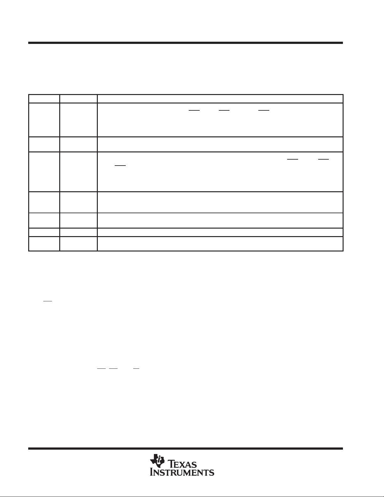
TMS320C203, TMS320C209, TMS320LC203
DIGITAL SIGNAL PROCESSORS
SPRS025B – JUNE 1995 – REVISED AUGUST 1998
memory (continued)
Table 13 shows the names, addresses, and functional descriptions of the TMS320C209 memory-mapped
registers.
Table 13. TMS320C209 Memory-Mapped Registers
NAME ADDRESS DESCRIPTION
Interrupt-mask register. IMR individually masks or enables the seven interrupts. The lower three bits align to the
three external interrupt pins (bit 0 ties to INT1
IMR DS@0004
GREG DS@0005
IFR DS@0006
TCR IS@FFFC
PRD IS@FFFD
TIM IS@FFFE Timer-counter register. TIM contains the current 16-bit count of the timer. Reset initializes the TIM to 0xFFFF.
WSGR IS@FFFF
Bits 4 and 5 are not used in the TMS320C209. Bit 6 is reserved for monitor mode emulation operations and should
always be set to 0 except in conjunction with emulation monitor operations. Bits 7–15 are not used in the
TMS320C209. IMR is set to 0 at reset.
Global memory allocation register. GREG specifies the size of the global memory space. GREG is set to 0 at
reset.
Interrupt-flag register . IFR indicates that the ’C2xx core has latched an interrupt pulse from one of the maskable
interrupts. The lower three bits align to the three external interrupt pins (bit 0 ties to INT1
bit 2 to INT3
should always be set to 0 except in conjunction with emulation monitor operations. A 1 indicates an active
interrupt in the respective interrupt location. Writing a 1 to the respective interrupt bit clears an active flag and
the respective pending interrupt. Writing a 1 to an inactive flag has no affect. IFR is set to 0 at reset.
Timer-control register. TCR contains the control bits that define the divide-down ratio, start/stop the timer, and
reload the period. Also contained in TCR is the current count in the prescaler. Reset initializes the timer
divide-down ratio to 0 and starts the timer.
Timer-period register. PRD contains the 16-bit period that is loaded into the timer counter when the counter
borrows or when the reload bit is activated. Reset initializes the PRD to 0xFFFF.
Wait-state generator register . WSGR contains the three control bits to enable a single wait state each of program,
data, and I/O space as well as the address-visibility-enable bit. Reset initializes WSGR to 0xF.
). Bit 3 ties to the timer interrupt. Bits 4–15 are reserved for monitor mode emulation operations and
, bit 1 to INT2, and bit 2 to INT3). Bit 3 ties to the timer interrupt.
, bit 1 to INT2, and
external interface
The TMS320C2xx can address up to 64K × 16 words of memory or registers in each of the program, data, and
I/O spaces. On-chip memory, when enabled, removes some of this off-chip range. In data space, the high
32K words can be dynamically mapped either locally or globally using the GREG register as described in the
TMS320C2xx User’s Guide
BR
low (with timing similar to the address bus) (see Table 11).
The CPU of the TMS320C2xx schedules a program-fetch, data-read, and data-write on the same machine
cycle. This is because from on-chip memory, the CPU can execute all three of these operations in the same
cycle. However, the external interface multiplexes the internal buses to one address bus and one data bus. The
external interface sequences these operations to complete first the data-write, then the data-read, and finally
the program-read.
The ’C2xx supports a wide range of system-interfacing requirements. Program, data, and I/O address spaces
provide interface to memory and I/O, thereby maximizing system throughput. The full 16-bit address and data
bus, along with the PS
three spaces.
I/O design is simplified by having I/O treated the same way as memory. I/O devices are mapped into the I/O
address space using the processor’s external address and data buses in the same manner as memory-mapped
devices.
(literature number SPRU127). A data-memory access mapped as global asserts
, DS, and IS space-select signals, allow addressing of 64K 16-bit words in each of the
24
POST OFFICE BOX 1443 • HOUSTON, TEXAS 77251–1443

TMS320C203, TMS320C209, TMS320LC203
DIGITAL SIGNAL PROCESSORS
SPRS025B – JUNE 1995 – REVISED AUGUST 1998
external interface (continued)
The ’C2xx external parallel interface provides various control signals to facilitate interfacing to the device. The
R/W
output signal is provided to indicate whether the current cycle is a read or a write. The STRB output signal
provides a timing reference for all external cycles. For convenience, the device also provides the RD
WE
output signals, which indicate a read and a write cycle, respectively , along with timing information for those
cycles. The availability of these signals minimizes external gating necessary for interfacing external devices to
the ’C2xx.
Interface to memory and I/O devices of varying speeds is accomplished by using the READY line. When
transactions are made with slower devices, the ’C2xx processor waits until the other device completes its
function and signals the processor by way of the READY line. Once a ready indication is provided back to the
’C2xx from the external device, execution continues. On the ’C209 device, the READY line is required (active
high) to complete reads or writes to internal I/O-mapped registers. On the ’C203 devices, the READY
line is required to be active high during boot time.
and the
The bus-request (BR
global-memory accesses. Global memory is external data-memory space in which the BR
at the beginning of the access. When an external global-memory device receives the bus request, it responds
by asserting the READY signal after the global memory access is arbitrated and the global access is completed.
The TMS320C2xx supports zero-wait-state reads on the external interface. However, to avoid bus conflicts,
writes take two cycles. This allows the TMS320C2xx to buffer the transition of the data bus from input to output
(or output to input) by a half cycle. In most systems, TMS320C2xx ratio of reads to writes is significantly large
to minimize the overhead of the extra cycle on writes.
Wait states can be generated when accessing slower external resources. The wait states operate on
machine-cycle boundaries and are initiated either by using READY or by using the software wait-state
generator. READY can be used to generate any number of wait states.
) signal is used in conjunction with the other ’C2xx interface signals to arbitrate external
signal is asserted
interrupts and subroutines
The ’C2xx implements three general-purpose interrupts, INT3–INT1, along with reset (RS) and the
nonmaskable interrupt (NMI
Internal interrupts are generated by the synchronous serial port (RINT and XINT) (’C203 only), the
asynchronous serial port (TXRXINT) (’C203 only), the timer (TINT), the UART, and the software-interrupt
(TRAP, INTR and NMI) instructions. Interrupts are prioritized with RS
NMI
, and timer (TINT) (for ’C209) or UART (for ’C203) having the lowest priority. Additionally, any interrupt,
except RS
can be cleared, set, or tested using its own dedicated bit in the interrupt flag register (IFR). The reset and NMI
functions are not maskable.
and NMI, can be individually masked with a dedicated bit in the interrupt mask register (IMR) and
), which are available for external devices to request the attention of the processor.
having the highest priority, followed by
All interrupt vector locations are on two-word boundaries so that branch instructions can be accommodated in
those locations if desired.
A built-in mechanism protects multicycle instructions from interrupts. If an interrupt occurs during a multicycle
instruction, the interrupt is not processed until the instruction completes execution. This mechanism applies to
instructions that are repeated (using the RPT instruction) and to instructions that become multicycle because
of wait states.
Each time an interrupt is serviced or a subroutine is entered, the program counter (PC) is pushed onto an internal
hardware stack, providing a mechanism for returning to the previous context. The stack contains eight locations,
allowing interrupts or subroutines to be nested up to eight-levels deep.
POST OFFICE BOX 1443 • HOUSTON, TEXAS 77251–1443
25
 Loading...